EP0604921B1 - Liquid crystal device and liquid crystal display apparatus - Google Patents
Liquid crystal device and liquid crystal display apparatus Download PDFInfo
- Publication number
- EP0604921B1 EP0604921B1 EP93120832A EP93120832A EP0604921B1 EP 0604921 B1 EP0604921 B1 EP 0604921B1 EP 93120832 A EP93120832 A EP 93120832A EP 93120832 A EP93120832 A EP 93120832A EP 0604921 B1 EP0604921 B1 EP 0604921B1
- Authority
- EP
- European Patent Office
- Prior art keywords
- liquid crystal
- temperature
- chiral smectic
- angle
- alignment
- Prior art date
- Legal status (The legal status is an assumption and is not a legal conclusion. Google has not performed a legal analysis and makes no representation as to the accuracy of the status listed.)
- Expired - Lifetime
Links
- 0 Cc(cc1)cc2c1NC(*)C*2 Chemical compound Cc(cc1)cc2c1NC(*)C*2 0.000 description 1
Images


Classifications
-
- G—PHYSICS
- G02—OPTICS
- G02F—OPTICAL DEVICES OR ARRANGEMENTS FOR THE CONTROL OF LIGHT BY MODIFICATION OF THE OPTICAL PROPERTIES OF THE MEDIA OF THE ELEMENTS INVOLVED THEREIN; NON-LINEAR OPTICS; FREQUENCY-CHANGING OF LIGHT; OPTICAL LOGIC ELEMENTS; OPTICAL ANALOGUE/DIGITAL CONVERTERS
- G02F1/00—Devices or arrangements for the control of the intensity, colour, phase, polarisation or direction of light arriving from an independent light source, e.g. switching, gating or modulating; Non-linear optics
- G02F1/01—Devices or arrangements for the control of the intensity, colour, phase, polarisation or direction of light arriving from an independent light source, e.g. switching, gating or modulating; Non-linear optics for the control of the intensity, phase, polarisation or colour
- G02F1/13—Devices or arrangements for the control of the intensity, colour, phase, polarisation or direction of light arriving from an independent light source, e.g. switching, gating or modulating; Non-linear optics for the control of the intensity, phase, polarisation or colour based on liquid crystals, e.g. single liquid crystal display cells
- G02F1/137—Devices or arrangements for the control of the intensity, colour, phase, polarisation or direction of light arriving from an independent light source, e.g. switching, gating or modulating; Non-linear optics for the control of the intensity, phase, polarisation or colour based on liquid crystals, e.g. single liquid crystal display cells characterised by the electro-optical or magneto-optical effect, e.g. field-induced phase transition, orientation effect, guest-host interaction or dynamic scattering
- G02F1/139—Devices or arrangements for the control of the intensity, colour, phase, polarisation or direction of light arriving from an independent light source, e.g. switching, gating or modulating; Non-linear optics for the control of the intensity, phase, polarisation or colour based on liquid crystals, e.g. single liquid crystal display cells characterised by the electro-optical or magneto-optical effect, e.g. field-induced phase transition, orientation effect, guest-host interaction or dynamic scattering based on orientation effects in which the liquid crystal remains transparent
- G02F1/141—Devices or arrangements for the control of the intensity, colour, phase, polarisation or direction of light arriving from an independent light source, e.g. switching, gating or modulating; Non-linear optics for the control of the intensity, phase, polarisation or colour based on liquid crystals, e.g. single liquid crystal display cells characterised by the electro-optical or magneto-optical effect, e.g. field-induced phase transition, orientation effect, guest-host interaction or dynamic scattering based on orientation effects in which the liquid crystal remains transparent using ferroelectric liquid crystals
- G02F1/1416—Details of the smectic layer structure, e.g. bookshelf, chevron, C1 and C2
-
- C—CHEMISTRY; METALLURGY
- C09—DYES; PAINTS; POLISHES; NATURAL RESINS; ADHESIVES; COMPOSITIONS NOT OTHERWISE PROVIDED FOR; APPLICATIONS OF MATERIALS NOT OTHERWISE PROVIDED FOR
- C09K—MATERIALS FOR MISCELLANEOUS APPLICATIONS, NOT PROVIDED FOR ELSEWHERE
- C09K19/00—Liquid crystal materials
- C09K19/04—Liquid crystal materials characterised by the chemical structure of the liquid crystal components, e.g. by a specific unit
- C09K19/06—Non-steroidal liquid crystal compounds
- C09K19/34—Non-steroidal liquid crystal compounds containing at least one heterocyclic ring
- C09K19/3441—Non-steroidal liquid crystal compounds containing at least one heterocyclic ring having nitrogen as hetero atom
- C09K19/345—Non-steroidal liquid crystal compounds containing at least one heterocyclic ring having nitrogen as hetero atom the heterocyclic ring being a six-membered aromatic ring containing two nitrogen atoms
- C09K19/3452—Pyrazine
-
- C—CHEMISTRY; METALLURGY
- C09—DYES; PAINTS; POLISHES; NATURAL RESINS; ADHESIVES; COMPOSITIONS NOT OTHERWISE PROVIDED FOR; APPLICATIONS OF MATERIALS NOT OTHERWISE PROVIDED FOR
- C09K—MATERIALS FOR MISCELLANEOUS APPLICATIONS, NOT PROVIDED FOR ELSEWHERE
- C09K19/00—Liquid crystal materials
- C09K19/04—Liquid crystal materials characterised by the chemical structure of the liquid crystal components, e.g. by a specific unit
- C09K19/06—Non-steroidal liquid crystal compounds
- C09K19/34—Non-steroidal liquid crystal compounds containing at least one heterocyclic ring
- C09K19/3441—Non-steroidal liquid crystal compounds containing at least one heterocyclic ring having nitrogen as hetero atom
- C09K19/345—Non-steroidal liquid crystal compounds containing at least one heterocyclic ring having nitrogen as hetero atom the heterocyclic ring being a six-membered aromatic ring containing two nitrogen atoms
- C09K19/3458—Uncondensed pyrimidines
- C09K19/3466—Pyrimidine with at least another heterocycle in the chain
Definitions
- This invention relates to a liquid crystal device to be used in a liquid crystal display device or a liquid crystal-optical shutter, etc., particularly a liquid crystal device using of a ferroelectric liquid crystal, and a liquid crystal display apparatus using the liquid crystal device.
- a display device of the type which controls transmission of light in combination with a polarizing device by utilizing the refractive index anisotropy of ferroelectric liquid crystal molecules has been proposed by Clark and Lagerwall (U.S. Patent No. 4,367,924, etc.).
- the ferroelectric liquid crystal has generally chiral smectic C phase (SmC*) or H phase (SmH*) of a non-helical structure and, in the SmC* or SmH* phase, shows a property of assuming either one of a first optically stable state and a second optically stable state responding to an electrical field applied thereto and maintaining such a state in the absence of an electrical field, namely bistability, and also has a quick responsiveness to the change in electrical field.
- SmC* chiral smectic C phase
- SmH* H phase
- bistability bistability
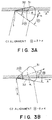
- an apparent tilt angle ⁇ a (a half of an angle formed between molecular axes at two stable states) in a ferroelectric liquid crystal with a non-helical structure obtained by alignment with an alignment control film of the prior art has become smaller as compared with a cone angle H ⁇ (the angle H ⁇ is a half of the apex angle of the cone shown in Figure 3A as described below) in the ferroelectric liquid crystal having a helical structure.
- the apparent tilt angle ⁇ a in a ferroelectric liquid crystal with a non-helical structure obtained by alignment with alignment control films of the prior art was found to be generally on the order of 3 - 8 degrees, and the transmittance at that time was at most about 3 to 5 %.
- a liquid crystal device comprising: a pair of substrates, and a chiral smectic liquid crystal disposed between the substrates, each of the facing surfaces of substrates having thereon an electrode for applying a voltage to the liquid crystal and a uniaxial alignment film for aligning the liquid crystal; wherein the alignment films on the substrates are provided with uniaxial alignment axes which cross each other at a prescribed angle and the chiral smectic liquid crystal is disposed in such an alignment state that the liquid crystal shows a pretilt angle ⁇ , a cone angle H ⁇ , and an inclination angle ⁇ of the liquid crystal layer (i.e., an angle formed by the liquid crystal layer line and a normal to the substrate) satisfying relationships of: H ⁇ ⁇ + ⁇ and ⁇ ⁇ ⁇ , and such an alignment state includes at least two stable states in which an apparent tilt angle ⁇ a and the cone angle H ⁇ sati
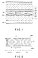
- a smectic liquid crystal generally has a layer structure and, due to a shrinkage of spacing between layers when it causes a transition from smectic A phase (SmA) to chiral smectic C phase (SmC*), it assumes a chevron structure as shown in Figure 2 where the layers 21 are bent at a mid point between a pair of substrates 24a and 24b.
- transition between two splay states is caused under application of weak positive and negative pulse electric fields
- transition between two uniform states is caused under application of strong positive and negative pulse electric fields.
- the two uniform states it is possible to realize a display device which is brighter and shows a higher contrast than the conventional devices. Accordingly, it is expected that a display with a higher quality can be realized by using a display device wherein the entire display area is formed in C1 alignment state and the high contrast two states in the C1 alignment state are used as two states representing white and black display states.
- condition for preventing the formation of C2 alignment but allowing C1 alignment is H ⁇ - ⁇ ⁇ ⁇ , that is H ⁇ ⁇ + ⁇
- a display apparatus using a chiral smectic liquid crystal can realize a large screen and a high resolution which by far exceed those attained by conventional CRT and TN-type liquid crystal displays.
- the frame frequency (frequency constituting one picture) becomes low. This leads to a problem that the picture-rewriting speed becomes slow and the motion picture display becomes slow, e.g., in cases of smooth scrolling and cursor movement on a graphic screen.
- a solution to this problem has been given in, e.g., JP-A 60-31120 and JP-A 1-140198.
- a display apparatus including a display panel comprising scanning electrodes and data electrodes arranged in a matrix, whole-area writing means for selecting all or a prescribed part of the scanning electrodes for writing and partial writing means for selecting a part of the above-mentioned all or a prescribed part of the scanning electrodes.
- a ferroelectric liquid crystal potentially has very excellent characteristics, and by making use of these properties, it is possible to provide essential improvements to many of the above-mentioned problems with the conventional TN-type devices.
- the application to a high-speed optical shutter and a display of a high density and a large picture is expected.
- ferroelectric liquid crystal materials developed heretofore cannot be said to satisfy sufficient characteristics required for a liquid crystal device including an operable temperature range, temperature-dependence of response speed, low-temperature storage properties, impact or shock resistance, etc. in some cases.
- a ferroelectric liquid crystal has a clear layer structure at a temperature range where the ferroelectric liquid crystal is used, thus showing a poor flowability compared with a nematic liquid crystal. Accordingly, the ferroelectric liquid crystal has a relatively poor brittleness against an external stress such as a force of shock or strain and thus causes a zigzag defect comprising C1 alignment and C2 alignment for a slight shock. For a great shock, the ferroelectric liquid crystal causes a disorder of its layer structure per se, thus resulting in, e.g., a sanded texture as disclosed in U.S. Patent No. 4,674,839 by Tsuboyama et al.
- a shock (or impact) resistance is liable to become worse at a low temperature where a viscosity of a liquid crystal is increased to provide a poor flowability, resulting in a serious problem in the case of transportation by aircraft etc.
- a lower limit temperature to chiral smectic C phase i.e., a phase transition temperature (Mp) to another mesomorphic phase or crystal phase is an essential factor for determining low-temperature storage properties.
- an Mp of a liquid crystal composition having overall excellent characteristics including a high contrast and a decreased temperature-dependence of a response speed providing a high quality image in a wide temperature range including room temperature, to a sufficiently low temperature region (e.g., below -20 °C).
- EP-A-0 548 548 which represents prior art under Art. 54(3) EPC, discloses a liquid crystal device with a decreased temperature-dependence of response speed which is obtained by using a liquid crystal composition having a temperature range where the composition assumes chiral smectic C phase.
- EP-A-0 455 160 discloses a liquid crystal display device having fast response characteristics and enabling analog gray-scaled display.
- An object of the present invention is to provide a liquid crystal device having a good shock resistance particularly at low temperature and a liquid crystal display apparatus using the liquid crystal device.
- Another object of the present invention is to provide a liquid crystal device having an excellent low temperature storage properties and a liquid crystal display apparatus using the liquid crystal device.
- a liquid crystal device comprising a pair of substrates and a chiral smectic liquid crystal disposed between the pair of substrates, each of the substrates having thereon an electrode for applying a voltage to the liquid crystal, the pair of substrates being provided with respective uniaxial alignment axes extending in directions which are parallel to each other or intersect each other at a prescribed angle, wherein the chiral smectic liquid crystal is placed in such an alignment state that the liquid crystal molecules will have a single average molecular axis substantially aligned with a central axis direction of the uniaxial alignment axes under no electric field application on a lower temperature side within chiral smectic C phase range, wherein the single average molecular axis can be confirmed as a position providing the darkest state when observed through cross nicol polarizers, and the chiral smectic liquid crystal comprises a liquid crystal composition containing:
- a liquid crystal display apparatus comprising the above liquid crystal device, a drive circuit for driving the liquid crystal device and a light source.
- Figure 1 is a schematic sectional view of an embodiment of the liquid crystal device according to the present invention.
- Figure 2 is an illustration of C1 and C2 alignment states.
- Figures 3A and 3B are illustrations of relationship among a cone angle, a pretilt angle and a layer inclination angle in C1 alignment and C2 alignment, respectively.
- Figure 4 is a waveform diagram illustrating driving waveforms used in an embodiment of the present invention.
- Figure 5 is a plan view of an electrode matrix.
- Figure 6 is a block diagram of a liquid crystal display apparatus and a graphic controller.
- Figure 7 is a time chart showing time correlation for image data communication between the liquid crystal display apparatus and the graphic controller.
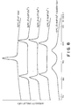
- Figure 8 is a graph of at some temperatures illustrating a change of a layer structure.
- the liquid crystal device according to the present invention is characterized by a chiral smectic liquid crystal capable of providing the above-mentioned specific alignment state on a lower temperature side within chiral smectic C phase.
- a quasi-smectic A alignment state is identified by an alignment state providing a single average molecular axis which can be confirmed as a position providing the darkest state when observed through cross nicol polarizers under no electric field application.
- the single average molecular axis extends in substantially the same direction as a central axis direction with respect to the uniaxial alignment axes in the above observation.
- a temperature providing such a single average molecular axis on temperature decrease is referred to as "quasi-S A state appearing temperature”.
- the liquid crystal device comprises a chiral smectic liquid crystal capable of providing a quasi-smectic A alignment state which appears at a temperature range lower than a temperature range where the chiral smectic liquid crystal assumes different two alignment states under no electric field application.
- the liquid crystal device may preferably include a chiral smectic liquid crystal being placed in such an alignment state that the liquid crystal assumes at least two stable states and provides a pretilt angle ⁇ , a cone angle H ⁇ , an inclination angle ⁇ of the liquid crystal layer, and an apparent tilt angle ⁇ a each in the neighborhood of room temperature satisfying the following relationships (1) and (2): H ⁇ ⁇ + ⁇ and ⁇ ⁇ ⁇ H > ⁇ a > H /2
- the liquid crystal device of the present invention may preferably have respective uniaxial alignment axes extending in directions which intersect each other at an angle of 1 - 25 degrees.
- the liquid crystal device of the present invention may preferably comprise the chiral smectic liquid crystal being further placed in such an alignment state that the liquid crystal molecules will have a single average molecular axis under no electric field application in the neighborhood of the upper limit temperature within chiral smectic C phase range, wherein the single average molecular axis can be confirmed as a position providing the darkest state when observed through cross nicol polarizers (Hereinbelow, such an alignment state is referred to as "another quasi-smectic A phase").
- the chiral smectic liquid crystal used in the present invention may preferably provide a pretilt angle ⁇ of at least 5 degrees.
- the chiral smectic liquid crystal may preferably have a temperature characteristic of an inclination angle ⁇ such that the inclination angle ⁇ increases on temperature decrease down to a mediate temperature as a temperature giving a maximum of inclination angle ⁇ and decreases on further temperature decrease below the mediate temperature.
- the mediate temperature may preferably appear at a temperature of at least 10 °C, more preferably at least 25 °C, in order to effectively improve a temperature-dependence of driving characteristics of the liquid crystal device at around room temperature.
- the chiral smectic liquid crystal may preferably have a relatively small inclination angle ⁇ providing a layer structure closer to a bookshelf state. At this time, the liquid crystal shows a cone angle H ⁇ smaller than one at room temperature in many cases.
- the quasi-smectic A alignment state appears at various temperature ranges depending upon a difference in, e.g., alignment treatment even when the same chiral smectic liquid crystal is used.
- a pretilt angle ⁇ is large, the quasi-smectic A alignment state is liable to appear at a relatively higher temperature on a low temperature side within Sc* (chiral smectic C phase) range.
- a value of the inclination angle ⁇ is changed depending upon values of pretilt angle ⁇ , cone angle H ⁇ , viscosity, etc.
- the value of the inclination angle ⁇ cannot not be referred to as an accurate numerical value but is about 6 degrees or below as an empirical value.
- the chiral smectic liquid crystal is placed in another quasi-smectic A alignment state at the neighborhood of the upper limit temperature of Sc* in many cases.
- the two alignment states can be distinguished by, e.g., measurement of cone angle H ⁇ at switching of the chiral smectic liquid crystal under electric field application.
- another quasi-smectic A alignment state cannot be said to be a state showing a memory characteristic because the liquid crystal molecules in one stable state are moved to align along a center axis direction of the uniaxial alignment axes at a velocity on the order of several milli-seconds.
- quasi-smectic A alignment state can be said to be a state showing a memory characteristic during a certain time because the movement of the liquid crystal molecules as described above is caused to occur at a velocity on the order of 0.1 second to several tens of seconds.
- the "quasi-smectic A alignment state" provides a liquid crystal device with an improved shock resistance and a stable alignment state causing no disorder of alignment caused by crystallization. This reason may be attributable to results obtained from X-ray diffraction experiment as follows.
- Figure 8 shows a graph of X-ray diffraction patterns of a liquid crystal composition (Composition D used in Example 2 - 5 appearing hereinafter) constituting a liquid crystal cell (cell gap: 1.2 ⁇ m, alignment film: "LQ-1802") for illustrating a change of layer structure at various temperatures (-10 °C, 10 °C, 30 °C, 50 °C and 70 °C).
- a liquid crystal composition Composition D used in Example 2 - 5 appearing hereinafter
- a liquid crystal cell cell gap: 1.2 ⁇ m, alignment film: "LQ-1802”
- Each X-ray diffraction pattern is obtained by scanning with respect to ⁇ axis on condition that an angle of 2 ⁇ is fixed at 3 degrees (corresponding to a layer spacing of 300 nm in Bragg condition).
- the sharp peaks (at 10 °C to 50 °C) on the diffraction patterns shows a longer correlation length (i.e., a longer orderly (or constant) layer distance) of the layer structure and the broad peaks (at -10 °C) shows a shorter correlation length (i.e., a shorter orderly layer distance) of the layer structure. That is, the peak shape in Sc* ⁇ quasi-S A phase transition at -10 o C is broader than that in Sc* at 10 to 50 °C. This reason is not clarified as yet but may be mainly attributable to an improvement in a flexibility of the layer structure in Sc* ⁇ quasi-S A phase transition. Such a layer structure in quasi-S A phase is presumably effective for absorbing an external shock.
- a value and a temperature dependence of a layer inclination angle ⁇ of a liquid crystal layer can be changed by controlling factors of liquid crystal compounds contained therein, such as a skeleton structure, side chain lengths and an affinity of combination.
- a type of a liquid crystal tending to provide a broader smectic A temperature range changes considerably the temperature dependence of ⁇ .
- the device includes a pair of substrates (glass plates) 11a and 11b coated with transparent electrodes 12a and 12b, respectively, of In 2 O 3 , ITO (indium tin oxide), etc., then with 200 to 3000 ⁇ -thick insulating films 13a and 13b, respectively, of SiO 2 , TiO 2 , Ta 2 O 5 , etc., and further with 50 to 1000 ⁇ -thick polyimide alignment films 14a and 14b formed, e.g., by applying and baking a polyamide acid represented by the following formula:
- the alignment films 14a and 14b are respectively provided with uniaxial alignment axes by rubbing in directions (denoted by arrows A in Figure 1) which are generally parallel and in the same direction but intersect each other at a clockwise or counter-clockwise angle of 0 - 25 degrees.
- the direction of clockwise (or counter-clockwise) intersection angle is determined herein by the direction of rotation of the alignment axis provided to the upper alignment film 14a from the alignment axis provided to the lower alignment film 14b as viewed from the upper substrate 11a.
- a chiral smectic C liquid crystal 15 Between the substrates 11a and 11b is disposed a chiral smectic C liquid crystal 15, and the spacing between the substrates 11a and 11b is set to a value (e.g., 0.1 - 3 ⁇ m) which is sufficiently small to suppress the formation of a helical structure of the chiral smectic C liquid crystal 15, thus resulting in bistable alignment states of the liquid crystal 15.
- the small spacing is held by spacer beads 16 of, e.g., silica or alumina, dispersed between the substrates.
- the thus-formed cell structure is sandwiched between a pair of polarizers 17a and 17b to provide a liquid crystal device.
- a simple matrix-type display apparatus using a liquid crystal device comprising a ferroelectric liquid crystal disposed between a pair of substrates as described above may be driven by driving methods as disclosed by, e.g., JP-A 59-193426, JP-A 59-193427, JP-A 60-156046 and JP-A 60-156047.
- Figure 4 is a waveform diagram showing an example set of driving waveforms used in such a driving method.
- Figure 5 is a plan view showing an electrode matrix used in a ferroelectric liquid crystal panel 51 of a simple matrix-type.
- the liquid crystal panel 51 shown in Figure 5 includes scanning electrodes 52 and data electrodes 53 intersecting each other so as to constitute a pixel at each intersection together with a ferroelectric liquid crystal disposed between the scanning electrodes 52 and data electrodes 53.
- a liquid crystal display apparatus may be constituted by using the liquid crystal device for a display panel and by adopting an arrangement and data format comprising image data accompanied with scanning line address data and also a communication synchronization scheme using a SYNC signal as shown in Figures 6 and 7.
- the liquid crystal display apparatus 101 includes a graphic controller 102, a display panel 103, a scanning line drive circuit 104, a data line drive circuit 105, a decoder 106, a scanning signal generator 107, a shift register 108, a line memory 109, a data signal generator 110, a drive control circuit 111, a graphic central processing unit (GCPU) 112, a host central processing unit (host CPU) 113, and an image data storage memory (VRAM) 114.
- Image data are generated in the graphic controller 102 in an apparatus body and transferred to the display panel 103 (illuminated with a backlight (not shown)) by signal transfer means shown in Figures 6 and 7.
- the graphic controller 102 principally comprises a CPU (or GCPU, central processing unit) 112 and a VRAM (video-RAM, image data storage memory) 114 and is in charge of management and communication of image data between a host CPU 113 and the liquid crystal display apparatus (FLCD) 101.
- the control of image display according to the present invention is principally accomplished by the graphic controller 102.
- a light source is disposed at the back of the display panel 103.
- cone angle H ⁇ apparent tilt angle ⁇ a, liquid crystal layer inclination angle ⁇ and pretilt angle ⁇ referred to herein are based on values measured according to the following methods.
- a liquid crystal device was sandwiched between right-angle crossed nicol polarizers and rotated horizontally relative to the polarizers under application of an AC voltage of ⁇ 30 V to ⁇ 50 V and 100 Hz between the upper and lower substrates of the device while measuring a transmittance through the device by a photomultiplier (available from Hamamatsu Photonics K.K.) to find a first extinct position (a position providing the lowest transmittance) and a second extinct position.
- a cone angle H ⁇ was measured as a half of the angle between the first and second extinct positions.
- a liquid crystal device sandwiched between right-angle crossed nicol polarizers was supplied with a single pulse of one polarity exceeding the threshold voltage of the ferroelectric liquid crystal and was then rotated under no electric field horizontally relative to the polarizers to find a first extinction position. Then, the liquid crystal device was supplied with a single pulse of the opposite polarity exceeding the threshold voltage of the ferroelectric liquid crystal and was then rotated under no electric field relative to the polarizers to find a second extinct position.
- An apparent tilt angle ⁇ a was measured as a half of the angle between the first and second extinct positions.
- the method used was basically similar to the method used by Clark and Largerwal (Japanese Display '86, Sept. 30 - Oct. 2, 1986, p.p. 456 - 458) or the method of Ohuchi et al (J.J.A.P., 27 (5) (1988), p.p. 725 - 728).
- the measurement was performed by using a rotary cathode-type X-ray diffraction apparatus (available from MAC Science), and 80 ⁇ m-thick microsheets (available from Corning Glass Works) were used as the substrates so as to minimize the X-ray absorption with the glass substrates of the liquid crystal cells.
- a pair of substrates rubbed in mutually parallel and opposite directions were applied to each other to form a cell having a cell gap of 20 ⁇ m, which was then filled with a liquid crystal mixture assuming SmA phase in the temperature range of 10 - 55 o C obtained by mixing 80 wt. % of a ferroelectric liquid crystal ("CS-1014", mfd. by Chisso K.K.) with 20 wt. % of a compound represented by the following formula:
- the liquid crystal cell was rotated in a plane perpendicular to the pair of substrates and including the aligning treatment axis and, during the rotation, the cell was illuminated with a helium-neon laser beam having a polarization plane forming an angle of 45 degrees with respect to the rotation plane in a direction normal to the rotation plane, whereby the intensity of the transmitted light was measured by a photodiode from the opposite side through a polarizer having a transmission axis parallel to the polarization plane.
- the chiral smectic liquid crystal used in the present invention comprises a liquid crystal composition containing at least one mesomorphic compound having the following structural formula (3): wherein R 1 denotes a linear or branched alkyl group having 1 - 18 carbon atoms; X 1 denotes a single bond, -O-, -COO- or -OCO-; X 2 denotes a single bond, -OCH 2 -, -COO- or -OCO-; n is an integer of 3 - 16; and A 1 denotes and at least one mesomorphic compound having the following formula (4): wherein R 2 and R 3 independently denote a linear or branched alkyl group having 1 - 18 carbon atoms; X 3 denotes a single bond, -O-, -OCO-, or -COO-; and A 2 denotes
- the chiral smectic liquid crystal used in the present invention is a liquid crystal composition comprising at least one mesomorphic compound of the formula (3) and at least one mesomorphic compound of the formula (4).
- the liquid crystal composition contains 1 - 30 wt. % in total of the mesomorphic compound of the formula (3) and 1 - 30 wt. % in total of the mesomorphic compound of the formula (4).
- mesomorphic compound of the formula (3) may include those shown in Table 1 below.
- mesomorphic compound of the formula (4) may include those shown in Table 1 below.
- a solution in NMP of a polyimide precursor ("LQ 1802" mfd. by Hitachi Kasei K.K. or "LP-64” mfd. by Toray K.K.) was applied onto the tantalum oxide film and baked at 200 - 270 o C (200 o C for LP-64, 270 °C for LQ-1802) -to form a 100 - 300 ⁇ -thick (100 ⁇ for LP-64, 300 ⁇ for LQ-1802) polyimide alignment film. The baked film was then rubbed with acetate fiber planted cloth. A pretilt angle is controlled by, e.g., changing rubbing conditions including a degree of pressing, rotation speed of a rubbing roller and a substrate feed velocity.
- epoxy resin adhesive particles having an average particle size of 5.5 ⁇ m (“Torepearl” (trade name), available from Toray K.K.) were dispersed at a density of 50 particles/mm 2 by the Nord Son electrostatic dispersion method and, on the other substrate, silica micro-beads having an average particle size of 1.2 ⁇ m were dispersed at a density of 300 particles/mm 2 by the Knudsen electrostatic dispersion method.
- a liquid adhesive (“Struct Bond” (trade name), mfd. by Mitsui Toatsu Kagaku K.K.) as a sealing member was applied by printing in a thickness of 6 ⁇ m.
- the two glass plates were applied to each other so that their rubbed directions extended generally in the same direction but intersected each other at a counterclockwise angle of 0 - 10 degrees, and bonded to each other by applying a pressure of 2,75 ⁇ 10 5 Pa (2.8 kg/cm 2 ) at 70 °C for 5 min, followed by further curing of the two types of adhesives under a pressure of 6,18 ⁇ 10 4 Pa (0.63 kg/cm 3 ) at 150 °C for 4 hours to form a blank cell.
- liquid crystal compositions A - H a ferroelectric liquid crystal (ZLI-3233", mfd. by Merk Co.), a ferroelectric liquid crystal ("CS-1014", mfd. by Chisso K.K.), respectively, to prepare liquid crystal devices.
- the liquid crystal compositions A - H were prepared by mixing mesomorphic compounds in prescribed proportions, respectively.
- the liquid crystal compositions G and H were prepared by mixing the following mesomorphic compounds in the indicated proportions below.
- Each of the liquid crystal compositions A - H and the ferroelectric liquid crystals (ZLI-3233 and CS-1014) was cooled to 30 o C providing chiral smectic C phase through phases including cholesteric phase and smectic A phase or smectic A phase.
- the liquid crystal compositions A - H and the ferroelectric liquid crystals showed the following properties including phase transition temperatures T PT (°C), spontaneous polarization Ps (nC/cm 2 ) at 30 °C, cone angle H ⁇ (degrees) at 30 °C, and inclination angle ⁇ (degrees) of a liquid crystal layer at various temperatures.
- T PT phase transition temperatures
- Ps and H ⁇ were shown in Table 3 below and the properties of ⁇ were shown in Table 4 below, respectively.
- the liquid crystal devices (Ex. 1-1 to 1-7) comprising the liquid crystal composition showing a quasi-smectic A alignment state on a lower temperature side (e.g., -11 o C to 3 °C) within chiral smectic C phase range provided a good shock resistance at 0 o C compared with those (Comp. Ex. 1-1 to 1-3) comprising the liquid crystal composition not showing a quasi-smectic A alignment state.
- each of the liquid crystal devices was cooled to -20 o C and kept at -20 o C for 100 hours, and then subjected to observation of an alignment state.
- the liquid crystal devices according to the present invention used in Examples 1-1 to 1-7 caused substantially no change in the alignment state.
- the liquid crystal devices used in Comparative Examples 1-1 to 1-3 i.e., not showing quasi-S A state
- the liquid crystal devices providing quasi-S A state according to the present invention stably showed a good shock resistance when compared with those failing to provide quasi-S A state.
- the liquid crystal devices (Ex. 3-1 to 3-5) comprising the liquid crystal composition showing a quasi-smectic A alignment state on a lower temperature side (e.g., -13 °C to 0 °C) within chiral smectic C phase range provided a good shock resistance at -5 °C compared with those (Comp. Ex. 3-1 to 3-2) comprising the liquid crystal composition not showing a quasi-smectic A alignment state.
- a liquid crystal device comprising a chiral smectic liquid crystal characterized by showing a quasi-smectic A alignment state (i.e., having a single average molecular axis) on a lower temperature side of chiral smectic C phase range when observed through cross nicol polarizers under no voltage application.
- a liquid crystal device provided a good shock resistance and low-temperature storage properties.
Description
- I0:
- incident light intensity,
- I:
- transmitted light intensity,
- a:
- apparent tilt angle,
- Δn:
- refractive index anisotropy,
- d:
- thickness of the liquid crystal layer,
- λ:
- wavelength of the incident light.


met = CH3, hep = C7H15, trd = C13H27,
eth = C2H5, oct = C8H17, tet = C14H29,
pro = C3H7, non = C9H19, ped = C15H31,
but = C4H9, dec = C10H21, hexd = C16H33,
pen = C5H11, und = C11H23, hepd = C17H35,
hex = C6H13, dod = C12H25, ocd = C18H37,
2mb = 2-methyl-butyl,


met = CH3, hep = C7H15, trd = C13H27,
eth = C2H5, oct = C8H17, tet = C14H29,
pro = C3H7, non = C9H19, ped = C15H31,
but = C4H9, dec = C10H21, hexd = C16H33,
pen = C5H11, und = C11H23, hepd = C17H35,
hex = C6H13, dod = C12H25, ocd = C18H37,
2mb = 2-methyl-butyl,


| L.C. | Layer inclination angle δ (deg.) | ||||||
| -10oC | 0oC | 10oC | 20oC | 30oC | 40oC | 50oC | |
| A | - | 6.1 | 8.9 | 10.3 | 10.4 | 8.7 | - |
| B | - | - | 6.2 | 8.9 | 10.0 | 10.5 | 9.7 |
| C | 5.4 | 8.5 | 11.0 | 12.2 | 12.8 | 12.6 | 11.4 |
| D | 1.4 | 5.9 | 8.1 | 9.6 | 10.2 | 10.3 | 9.6 |
| E | 4.6 | 7.3 | 8.8 | 10.0 | 10.7 | 10.7 | 10.0 |
| F | - | - | 12.4 | 12.5 | 12.3 | 11.4 | 9.6 |
| G | - | - | 4.8 | 7.8 | 9.3 | 9.8 | 9.4 |
| H | - | 4.8 | 7.6 | 9.4 | 10.6 | 11.0 | 10.0 |
| ZLI-3233 | 29.1 | 28.7 | 28.4 | 27.8 | 27.0 | 25.7 | 23.9 |
| CS-1014 | 15.5 | 17.7 | 18.8 | 19.1 | 18.5 | 16.6 | 12.5 |


Claims (9)
- A liquid crystal device, comprising: a pair of substrates (11a, 11b) and a chiral smectic liquid crystal (15) disposed between the pair of substrates (11a, 11b), each of the substrates having thereon an electrode (12a, 12b) for applying a voltage to the liquid crystal, the pair of substrates (12a, 12b) being provided with respective uniaxial alignment axes (14a, 14b) extending in directions which are parallel to each other or intersect each other at a prescribed angle, whereinthe chiral smectic liquid crystal is placed in such an alignment state that the liquid crystal molecules will have a single average molecular axis substantially aligned with a central axis direction of the uniaxial alignment axes under no electric field application on a lower temperature side within chiral smectic C phase range, wherein the single average molecular axis can be confirmed as a position providing the darkest state when observed through cross nicol polarizers (17a, 17b), and the chiral smectic liquid crystal comprises a liquid crystal composition containing:at least one mesomorphic compound having the following formula (3):wherein R1 denotes a linear or branched alkyl group having 1 - 18 carbon atoms; X1 denotes a single bond, -O-, -COO- or -OCO-; X2 denotes a single bond, -OCH2-, -COO- or -OCO-; n is an integer of 3 - 16; and A1 denotes

 and
and at least one mesomorphic compound having the following formula (4):wherein R2 and R3 independently denote a linear or branched alkyl group having 1 - 18 carbon atoms; X3 denotes a single bond, -O-, -OCO-, or -COO-; and A2 denotes
 the liquid crystal composition comprising 1 to 30 wt.-% in total of said mesomorphic compound of the formula (3) and 1 to 30 wt. % in total of said mesomorphic compound of the formula (4).
- A device according to claim 1, wherein the chiral smectic liquid crystal is placed in such an alignment state that the liquid crystal assumes at least two stable states and provides a pretilt angle α, a cone angle H ○, an inclination angle δ of the liquid crystal layer, and an apparent tilt angle a each in the neighborhood of room temperature satisfying the following relationships (1) and (2):
- A device according to claim 1 or 2, wherein the respective uniaxial alignment axes extend in directions intersecting each other at an angle of 1 to 25 degrees.
- A device according to any of claims 1 to 3, wherein the chiral smectic liquid crystal is placed in such an alignment state that the liquid crystal molecules will have a single average molecular axis under no electric field application in the neighborhood of the upper limit temperature within chiral smectic C phase range, wherein the single average molecular axis can be confirmed as a position providing the darkest state when observed through cross nicol polarizers.
- A device according to any of claims 2 to 4, wherein the chiral smectic liquid crystal provides a pretilt angle α of at least 5 degrees.
- A device according to any of claims 2 to 5, wherein the inclination angle δ increases on temperature decrease down to a mediate temperature and decreases on further temperature decrease below the mediate temperature.
- A device according to claim 6, wherein the mediate temperature appears at a temperature of at least 10°C.
- A device according to claim 6, wherein the mediate temperature appears at a temperature of at least 25°C.
- A liquid crystal display apparatus (101), comprising a liquid crystal device according to any of claims 1 to 8, a drive circuit for driving the liquid crystal device and a light source.
Applications Claiming Priority (2)
| Application Number | Priority Date | Filing Date | Title |
|---|---|---|---|
| JP357907/92 | 1992-12-25 | ||
| JP35790792 | 1992-12-25 |
Publications (2)
| Publication Number | Publication Date |
|---|---|
| EP0604921A1 EP0604921A1 (en) | 1994-07-06 |
| EP0604921B1 true EP0604921B1 (en) | 1998-04-29 |
Family
ID=18456555
Family Applications (1)
| Application Number | Title | Priority Date | Filing Date |
|---|---|---|---|
| EP93120832A Expired - Lifetime EP0604921B1 (en) | 1992-12-25 | 1993-12-23 | Liquid crystal device and liquid crystal display apparatus |
Country Status (3)
| Country | Link |
|---|---|
| US (2) | US5460749A (en) |
| EP (1) | EP0604921B1 (en) |
| DE (1) | DE69318276T2 (en) |
Families Citing this family (18)
| Publication number | Priority date | Publication date | Assignee | Title |
|---|---|---|---|---|
| DE4236104A1 (en) * | 1992-10-26 | 1994-04-28 | Hoechst Ag | Bifunctional primary products for the production of liquid crystals |
| JP3377826B2 (en) * | 1993-05-06 | 2003-02-17 | ヘキスト・アクチェンゲゼルシャフト | Novel compounds for use in liquid crystal compositions |
| GB2293889A (en) * | 1994-10-03 | 1996-04-10 | Sharp Kk | Liquid crystal device and method of making a liquid crystal device |
| US5728318A (en) * | 1994-11-10 | 1998-03-17 | Canon Kabushiki Kaisha | Liquid crystal composition, liquid crystal device and liquid crystal display apparatus |
| JPH08134452A (en) * | 1994-11-15 | 1996-05-28 | Hoechst Japan Ltd | Liquid crystal composition |
| JP3119340B2 (en) * | 1995-01-31 | 2000-12-18 | キヤノン株式会社 | Liquid crystal composition, liquid crystal element having the same, and liquid crystal device having the same |
| US5858273A (en) * | 1995-07-27 | 1999-01-12 | Canon Kabushiki Kaisha | Liquid crystal device |
| EP0768360B1 (en) * | 1995-10-12 | 2002-01-09 | Canon Kabushiki Kaisha | Liquid crystal composition, liquid crystal device, and liquid crystal display apparatus using same |
| JP3093627B2 (en) * | 1996-02-09 | 2000-10-03 | キヤノン株式会社 | Manufacturing method of liquid crystal display device |
| US6139927A (en) * | 1997-09-18 | 2000-10-31 | Canon Kabushiki Kaisha | Liquid crystal device |
| EP0909803A1 (en) * | 1997-10-17 | 1999-04-21 | Aventis Research & Technologies GmbH & Co. KG | Chiral smectic liquid crystal mixture |
| EP0916712A1 (en) * | 1997-10-28 | 1999-05-19 | Aventis Research & Technologies GmbH & Co. KG | Chiral smectic liquid crystal mixture containing 1,2-difluoronaphthalenes |
| US6417828B1 (en) | 1999-02-18 | 2002-07-09 | Canon Kabushiki Kaisha | Liquid crystal composition, liquid crystal device, driving method thereof and liquid crystal apparatus |
| US6888522B1 (en) * | 1999-03-31 | 2005-05-03 | Minolta Co., Ltd. | Information display apparatus |
| ES2389955T3 (en) * | 2004-04-30 | 2012-11-05 | Genentech, Inc. | Hedgehog signaling pathway quinoxaline inhibitors |
| US8083385B1 (en) * | 2007-10-26 | 2011-12-27 | Yongwu Yang | Sunlight attenuation visor |
| JP5121432B2 (en) * | 2007-12-11 | 2013-01-16 | キヤノン株式会社 | Liquid crystal display device, manufacturing method thereof, and liquid crystal projection device |
| KR20210132772A (en) * | 2020-04-27 | 2021-11-05 | 삼성디스플레이 주식회사 | Display device and method for manufacturing of the same |
Family Cites Families (23)
| Publication number | Priority date | Publication date | Assignee | Title |
|---|---|---|---|---|
| US4367924A (en) * | 1980-01-08 | 1983-01-11 | Clark Noel A | Chiral smectic C or H liquid crystal electro-optical device |
| USRE34966E (en) * | 1980-01-08 | 1995-06-13 | Clark Noel A | Surface stabilized ferroelectric liquid crystal devices with LC molecules aligned at angle Ω(α) from normal to substrates |
| JPS59193426A (en) * | 1983-04-19 | 1984-11-02 | Canon Inc | Driving method of optical modulating element |
| JPS6031120A (en) * | 1983-07-30 | 1985-02-16 | Canon Inc | Driving method of optical modulating element |
| JPS59193427A (en) * | 1983-04-19 | 1984-11-02 | Canon Inc | Driving method of optical modulating element |
| JPS60156046A (en) * | 1984-01-23 | 1985-08-16 | Canon Inc | Driving method of optical modulating element |
| JPS60156047A (en) * | 1984-01-23 | 1985-08-16 | Canon Inc | Driving method of optical modulating element |
| FR2590392B1 (en) * | 1985-09-04 | 1994-07-01 | Canon Kk | FERROELECTRIC LIQUID CRYSTAL DEVICE |
| JPS6259922A (en) * | 1985-09-10 | 1987-03-16 | Canon Inc | Ferroelectric liquid crystal element |
| JPS62278540A (en) * | 1986-05-27 | 1987-12-03 | Canon Inc | Liquid crystal element and its orientation control method and driving method |
| JPS6440198A (en) * | 1987-08-06 | 1989-02-10 | Kawasaki Steel Co | Method for controlling flux feeding of flux cored wire |
| US4932758A (en) * | 1987-09-17 | 1990-06-12 | Canon Kabushiki Kaisha | Ferroelectric smectic liquid crystal device having a bistable alignment state providing two stable orientation states |
| US5200848A (en) * | 1987-09-17 | 1993-04-06 | Canon Kabushiki Kaisha | Ferroelectric smectic liquid crystal device |
| US5293544A (en) * | 1989-03-07 | 1994-03-08 | Canon Kabushiki Kaisha | Liquid crystal apparatus including panel having plural bent layers of liquid crystal molecules |
| DE69131258T2 (en) * | 1990-03-02 | 2000-03-02 | Canon Kk | Liquid crystal element and liquid crystal device using this element |
| JP2982330B2 (en) * | 1990-04-28 | 1999-11-22 | ソニー株式会社 | Liquid crystal display device |
| JPH04255827A (en) * | 1991-02-08 | 1992-09-10 | Canon Inc | Liquid crystal element and display device |
| JPH04258924A (en) * | 1991-02-13 | 1992-09-14 | Canon Inc | Ferroelectric liquid crystal element |
| EP0539992B1 (en) * | 1991-10-30 | 1997-01-29 | Canon Kabushiki Kaisha | Liquid crystal device |
| DE69216548T2 (en) * | 1991-10-30 | 1997-07-31 | Canon Kk | Liquid crystal device and display device |
| ATE233800T1 (en) * | 1991-11-22 | 2003-03-15 | Canon Kk | LIQUID CRYSTAL COMPOSITION, LIQUID CRYSTAL DEVICE AND DISPLAY DEVICE |
| JP3100014B2 (en) * | 1991-12-10 | 2000-10-16 | キヤノン株式会社 | Ferroelectric liquid crystal device and method for manufacturing the device |
| US5467209A (en) * | 1992-01-24 | 1995-11-14 | Canon Kabushiki Kaisha | Ferroelectric liquid crystal device with particular layer thicknesses at non-pixel portions and pixel portions |
-
1993
- 1993-12-23 US US08/172,164 patent/US5460749A/en not_active Expired - Fee Related
- 1993-12-23 EP EP93120832A patent/EP0604921B1/en not_active Expired - Lifetime
- 1993-12-23 DE DE69318276T patent/DE69318276T2/en not_active Expired - Fee Related
-
1995
- 1995-06-07 US US08/475,533 patent/US5657141A/en not_active Expired - Fee Related
Also Published As
| Publication number | Publication date |
|---|---|
| US5657141A (en) | 1997-08-12 |
| DE69318276T2 (en) | 1998-10-08 |
| US5460749A (en) | 1995-10-24 |
| DE69318276D1 (en) | 1998-06-04 |
| EP0604921A1 (en) | 1994-07-06 |
Similar Documents
| Publication | Publication Date | Title |
|---|---|---|
| EP0604921B1 (en) | Liquid crystal device and liquid crystal display apparatus | |
| EP0770662B1 (en) | Liquid crystal composition, liquid crystal device and display apparatus | |
| EP0647695B1 (en) | Liquid crystal composition, liquid crystal device and liquid crystal apparatus using same | |
| EP0711818B1 (en) | Liquid crystal composition, liquid crystal device and liquid crystal display apparatus | |
| JP3119341B2 (en) | Liquid crystal composition, liquid crystal element having the same, and liquid crystal device having the same | |
| JP3119342B2 (en) | Liquid crystal composition, liquid crystal element having the same, and liquid crystal device having the same | |
| JP3043257B2 (en) | Liquid crystal composition, liquid crystal element having the same, and liquid crystal device having the same | |
| JP3119340B2 (en) | Liquid crystal composition, liquid crystal element having the same, and liquid crystal device having the same | |
| JP3119339B2 (en) | Liquid crystal element and liquid crystal device having the same | |
| JP3060146B2 (en) | Liquid crystal element and liquid crystal display | |
| JPH07159790A (en) | Ferroelectric liquid crystal element and liquid crystal display device with the same | |
| JP3585186B2 (en) | Liquid crystal composition, liquid crystal element having the same, and liquid crystal device having the same | |
| JP3585183B2 (en) | Liquid crystal composition, liquid crystal element having the same, and liquid crystal device having the same | |
| JP3585184B2 (en) | Liquid crystal composition, liquid crystal element having the same, and liquid crystal device having the same | |
| JP3221539B2 (en) | Liquid crystal element, liquid crystal device using the same, and liquid crystal display device | |
| JP3585187B2 (en) | Liquid crystal composition, liquid crystal element having the same, and liquid crystal device having the same | |
| JP3585185B2 (en) | Liquid crystal composition, liquid crystal element having the same, and liquid crystal device having the same | |
| JPH08209135A (en) | Liquid crystal composition, liquid crystal element containing the same and liquid device containing the same | |
| JPH08209131A (en) | Liquid crystal composition, liquid crystal element containing the same and liquid crystal device containing the same | |
| JPH08209133A (en) | Liquid crystal composition, liquid crystal element containing the same and liquid crystal device containing the same | |
| JPH08225784A (en) | Liquid crystal composition and liquid crystal element and liquid crystal device using the same |
Legal Events
| Date | Code | Title | Description |
|---|---|---|---|
| PUAI | Public reference made under article 153(3) epc to a published international application that has entered the european phase |
Free format text: ORIGINAL CODE: 0009012 |
|
| 17P | Request for examination filed |
Effective date: 19931223 |
|
| AK | Designated contracting states |
Kind code of ref document: A1 Designated state(s): DE ES FR GB IT NL SE |
|
| 17Q | First examination report despatched |
Effective date: 19960628 |
|
| GRAG | Despatch of communication of intention to grant |
Free format text: ORIGINAL CODE: EPIDOS AGRA |
|
| GRAG | Despatch of communication of intention to grant |
Free format text: ORIGINAL CODE: EPIDOS AGRA |
|
| GRAH | Despatch of communication of intention to grant a patent |
Free format text: ORIGINAL CODE: EPIDOS IGRA |
|
| GRAH | Despatch of communication of intention to grant a patent |
Free format text: ORIGINAL CODE: EPIDOS IGRA |
|
| GRAA | (expected) grant |
Free format text: ORIGINAL CODE: 0009210 |
|
| AK | Designated contracting states |
Kind code of ref document: B1 Designated state(s): DE ES FR GB IT NL SE |
|
| PG25 | Lapsed in a contracting state [announced via postgrant information from national office to epo] |
Ref country code: IT Free format text: LAPSE BECAUSE OF FAILURE TO SUBMIT A TRANSLATION OF THE DESCRIPTION OR TO PAY THE FEE WITHIN THE PRESCRIBED TIME-LIMIT;WARNING: LAPSES OF ITALIAN PATENTS WITH EFFECTIVE DATE BEFORE 2007 MAY HAVE OCCURRED AT ANY TIME BEFORE 2007. THE CORRECT EFFECTIVE DATE MAY BE DIFFERENT FROM THE ONE RECORDED. Effective date: 19980429 Ref country code: ES Free format text: THE PATENT HAS BEEN ANNULLED BY A DECISION OF A NATIONAL AUTHORITY Effective date: 19980429 |
|
| REF | Corresponds to: |
Ref document number: 69318276 Country of ref document: DE Date of ref document: 19980604 |
|
| ET | Fr: translation filed | ||
| PG25 | Lapsed in a contracting state [announced via postgrant information from national office to epo] |
Ref country code: SE Free format text: LAPSE BECAUSE OF FAILURE TO SUBMIT A TRANSLATION OF THE DESCRIPTION OR TO PAY THE FEE WITHIN THE PRESCRIBED TIME-LIMIT Effective date: 19980729 |
|
| PLBE | No opposition filed within time limit |
Free format text: ORIGINAL CODE: 0009261 |
|
| STAA | Information on the status of an ep patent application or granted ep patent |
Free format text: STATUS: NO OPPOSITION FILED WITHIN TIME LIMIT |
|
| 26N | No opposition filed | ||
| REG | Reference to a national code |
Ref country code: GB Ref legal event code: IF02 |
|
| PGFP | Annual fee paid to national office [announced via postgrant information from national office to epo] |
Ref country code: FR Payment date: 20021210 Year of fee payment: 10 |
|
| PGFP | Annual fee paid to national office [announced via postgrant information from national office to epo] |
Ref country code: GB Payment date: 20021218 Year of fee payment: 10 |
|
| PGFP | Annual fee paid to national office [announced via postgrant information from national office to epo] |
Ref country code: NL Payment date: 20021227 Year of fee payment: 10 |
|
| PGFP | Annual fee paid to national office [announced via postgrant information from national office to epo] |
Ref country code: DE Payment date: 20021231 Year of fee payment: 10 |
|
| PG25 | Lapsed in a contracting state [announced via postgrant information from national office to epo] |
Ref country code: GB Free format text: LAPSE BECAUSE OF NON-PAYMENT OF DUE FEES Effective date: 20031223 |
|
| PG25 | Lapsed in a contracting state [announced via postgrant information from national office to epo] |
Ref country code: NL Free format text: LAPSE BECAUSE OF NON-PAYMENT OF DUE FEES Effective date: 20040701 Ref country code: DE Free format text: LAPSE BECAUSE OF NON-PAYMENT OF DUE FEES Effective date: 20040701 |
|
| GBPC | Gb: european patent ceased through non-payment of renewal fee |
Effective date: 20031223 |
|
| PG25 | Lapsed in a contracting state [announced via postgrant information from national office to epo] |
Ref country code: FR Free format text: LAPSE BECAUSE OF NON-PAYMENT OF DUE FEES Effective date: 20040831 |
|
| NLV4 | Nl: lapsed or anulled due to non-payment of the annual fee |
Effective date: 20040701 |
|
| REG | Reference to a national code |
Ref country code: FR Ref legal event code: ST |