EP0604801A2 - Thin film heterojunction solar cell - Google Patents
Thin film heterojunction solar cell Download PDFInfo
- Publication number
- EP0604801A2 EP0604801A2 EP93119798A EP93119798A EP0604801A2 EP 0604801 A2 EP0604801 A2 EP 0604801A2 EP 93119798 A EP93119798 A EP 93119798A EP 93119798 A EP93119798 A EP 93119798A EP 0604801 A2 EP0604801 A2 EP 0604801A2
- Authority
- EP
- European Patent Office
- Prior art keywords
- zinc
- semiconductor film
- process according
- film
- solution
- Prior art date
- Legal status (The legal status is an assumption and is not a legal conclusion. Google has not performed a legal analysis and makes no representation as to the accuracy of the status listed.)
- Granted
Links
- 239000010409 thin film Substances 0.000 title claims abstract description 11
- XLOMVQKBTHCTTD-UHFFFAOYSA-N Zinc monoxide Chemical compound [Zn]=O XLOMVQKBTHCTTD-UHFFFAOYSA-N 0.000 claims abstract description 64
- 239000010408 film Substances 0.000 claims abstract description 44
- 239000004065 semiconductor Substances 0.000 claims abstract description 39
- VHUUQVKOLVNVRT-UHFFFAOYSA-N Ammonium hydroxide Chemical compound [NH4+].[OH-] VHUUQVKOLVNVRT-UHFFFAOYSA-N 0.000 claims abstract description 35
- 239000011787 zinc oxide Substances 0.000 claims abstract description 32
- ZOIORXHNWRGPMV-UHFFFAOYSA-N acetic acid;zinc Chemical compound [Zn].CC(O)=O.CC(O)=O ZOIORXHNWRGPMV-UHFFFAOYSA-N 0.000 claims abstract description 22
- 239000004246 zinc acetate Substances 0.000 claims abstract description 22
- 229910021511 zinc hydroxide Inorganic materials 0.000 claims abstract description 18
- 239000000908 ammonium hydroxide Substances 0.000 claims abstract description 15
- UGZADUVQMDAIAO-UHFFFAOYSA-L zinc hydroxide Chemical compound [OH-].[OH-].[Zn+2] UGZADUVQMDAIAO-UHFFFAOYSA-L 0.000 claims abstract description 13
- 229940007718 zinc hydroxide Drugs 0.000 claims abstract description 13
- 229910052751 metal Inorganic materials 0.000 claims abstract description 10
- 239000002184 metal Substances 0.000 claims abstract description 10
- NWONKYPBYAMBJT-UHFFFAOYSA-L zinc sulfate Chemical compound [Zn+2].[O-]S([O-])(=O)=O NWONKYPBYAMBJT-UHFFFAOYSA-L 0.000 claims abstract description 9
- 238000000151 deposition Methods 0.000 claims abstract description 8
- 238000000137 annealing Methods 0.000 claims abstract description 7
- 239000008139 complexing agent Substances 0.000 claims abstract description 6
- 235000013904 zinc acetate Nutrition 0.000 claims abstract description 6
- JIAARYAFYJHUJI-UHFFFAOYSA-L zinc dichloride Chemical compound [Cl-].[Cl-].[Zn+2] JIAARYAFYJHUJI-UHFFFAOYSA-L 0.000 claims abstract description 6
- 235000009529 zinc sulphate Nutrition 0.000 claims abstract description 6
- 239000011686 zinc sulphate Substances 0.000 claims abstract description 6
- 235000005074 zinc chloride Nutrition 0.000 claims abstract description 3
- 239000011592 zinc chloride Substances 0.000 claims abstract description 3
- GSEJCLTVZPLZKY-UHFFFAOYSA-N Triethanolamine Chemical compound OCCN(CCO)CCO GSEJCLTVZPLZKY-UHFFFAOYSA-N 0.000 claims description 25
- KTSFMFGEAAANTF-UHFFFAOYSA-N [Cu].[Se].[Se].[In] Chemical compound [Cu].[Se].[Se].[In] KTSFMFGEAAANTF-UHFFFAOYSA-N 0.000 claims description 23
- 238000000034 method Methods 0.000 claims description 22
- 230000008569 process Effects 0.000 claims description 18
- 229910044991 metal oxide Inorganic materials 0.000 claims description 11
- 150000004706 metal oxides Chemical class 0.000 claims description 11
- 150000003751 zinc Chemical class 0.000 claims description 9
- 239000011701 zinc Substances 0.000 claims description 9
- 229910000368 zinc sulfate Inorganic materials 0.000 claims description 6
- 150000001875 compounds Chemical class 0.000 claims description 4
- -1 01M zinc salt Chemical class 0.000 claims description 3
- HCHKCACWOHOZIP-UHFFFAOYSA-N Zinc Chemical compound [Zn] HCHKCACWOHOZIP-UHFFFAOYSA-N 0.000 claims description 3
- 229910052725 zinc Inorganic materials 0.000 claims description 3
- 229960001763 zinc sulfate Drugs 0.000 claims description 3
- QGZKDVFQNNGYKY-UHFFFAOYSA-O Ammonium Chemical compound [NH4+] QGZKDVFQNNGYKY-UHFFFAOYSA-O 0.000 claims description 2
- 238000002156 mixing Methods 0.000 claims description 2
- 210000004027 cell Anatomy 0.000 description 31
- 235000011114 ammonium hydroxide Nutrition 0.000 description 28
- WUPHOULIZUERAE-UHFFFAOYSA-N 3-(oxolan-2-yl)propanoic acid Chemical compound OC(=O)CCC1CCCO1 WUPHOULIZUERAE-UHFFFAOYSA-N 0.000 description 23
- 229910052980 cadmium sulfide Inorganic materials 0.000 description 23
- 238000002474 experimental method Methods 0.000 description 19
- 239000000758 substrate Substances 0.000 description 15
- 238000012360 testing method Methods 0.000 description 10
- 239000000126 substance Substances 0.000 description 8
- 238000007598 dipping method Methods 0.000 description 6
- IJGRMHOSHXDMSA-UHFFFAOYSA-N Atomic nitrogen Chemical compound N#N IJGRMHOSHXDMSA-UHFFFAOYSA-N 0.000 description 4
- 239000000956 alloy Substances 0.000 description 4
- 230000000694 effects Effects 0.000 description 4
- 229910052793 cadmium Inorganic materials 0.000 description 3
- BDOSMKKIYDKNTQ-UHFFFAOYSA-N cadmium atom Chemical compound [Cd] BDOSMKKIYDKNTQ-UHFFFAOYSA-N 0.000 description 3
- DVRDHUBQLOKMHZ-UHFFFAOYSA-N chalcopyrite Chemical compound [S-2].[S-2].[Fe+2].[Cu+2] DVRDHUBQLOKMHZ-UHFFFAOYSA-N 0.000 description 3
- 229910052951 chalcopyrite Inorganic materials 0.000 description 3
- 238000004519 manufacturing process Methods 0.000 description 3
- 239000000463 material Substances 0.000 description 3
- 239000002244 precipitate Substances 0.000 description 3
- 231100000331 toxic Toxicity 0.000 description 3
- 230000002588 toxic effect Effects 0.000 description 3
- MARUHZGHZWCEQU-UHFFFAOYSA-N 5-phenyl-2h-tetrazole Chemical compound C1=CC=CC=C1C1=NNN=N1 MARUHZGHZWCEQU-UHFFFAOYSA-N 0.000 description 2
- 238000013459 approach Methods 0.000 description 2
- 230000015572 biosynthetic process Effects 0.000 description 2
- 230000006872 improvement Effects 0.000 description 2
- 229910052757 nitrogen Inorganic materials 0.000 description 2
- 238000000682 scanning probe acoustic microscopy Methods 0.000 description 2
- XOLBLPGZBRYERU-UHFFFAOYSA-N tin dioxide Chemical compound O=[Sn]=O XOLBLPGZBRYERU-UHFFFAOYSA-N 0.000 description 2
- 210000003771 C cell Anatomy 0.000 description 1
- GYHNNYVSQQEPJS-UHFFFAOYSA-N Gallium Chemical compound [Ga] GYHNNYVSQQEPJS-UHFFFAOYSA-N 0.000 description 1
- ZOKXTWBITQBERF-UHFFFAOYSA-N Molybdenum Chemical compound [Mo] ZOKXTWBITQBERF-UHFFFAOYSA-N 0.000 description 1
- 241000276498 Pollachius virens Species 0.000 description 1
- UCKMPCXJQFINFW-UHFFFAOYSA-N Sulphide Chemical compound [S-2] UCKMPCXJQFINFW-UHFFFAOYSA-N 0.000 description 1
- 239000005083 Zinc sulfide Substances 0.000 description 1
- 229910007696 ZnSnO4 Inorganic materials 0.000 description 1
- 239000006096 absorbing agent Substances 0.000 description 1
- 230000009471 action Effects 0.000 description 1
- 229910045601 alloy Inorganic materials 0.000 description 1
- UYJXRRSPUVSSMN-UHFFFAOYSA-P ammonium sulfide Chemical compound [NH4+].[NH4+].[S-2] UYJXRRSPUVSSMN-UHFFFAOYSA-P 0.000 description 1
- 238000004458 analytical method Methods 0.000 description 1
- 230000004888 barrier function Effects 0.000 description 1
- 238000004140 cleaning Methods 0.000 description 1
- 238000000354 decomposition reaction Methods 0.000 description 1
- 230000003247 decreasing effect Effects 0.000 description 1
- 230000018044 dehydration Effects 0.000 description 1
- 238000006297 dehydration reaction Methods 0.000 description 1
- 238000005137 deposition process Methods 0.000 description 1
- 238000011161 development Methods 0.000 description 1
- 230000018109 developmental process Effects 0.000 description 1
- 238000000113 differential scanning calorimetry Methods 0.000 description 1
- 238000004090 dissolution Methods 0.000 description 1
- 238000001035 drying Methods 0.000 description 1
- 238000005530 etching Methods 0.000 description 1
- 238000001704 evaporation Methods 0.000 description 1
- 230000008020 evaporation Effects 0.000 description 1
- 229910052733 gallium Inorganic materials 0.000 description 1
- 239000011521 glass Substances 0.000 description 1
- XLYOFNOQVPJJNP-UHFFFAOYSA-M hydroxide Chemical group [OH-] XLYOFNOQVPJJNP-UHFFFAOYSA-M 0.000 description 1
- 238000007654 immersion Methods 0.000 description 1
- PJXISJQVUVHSOJ-UHFFFAOYSA-N indium(III) oxide Inorganic materials [O-2].[O-2].[O-2].[In+3].[In+3] PJXISJQVUVHSOJ-UHFFFAOYSA-N 0.000 description 1
- 229910052750 molybdenum Inorganic materials 0.000 description 1
- 239000011733 molybdenum Substances 0.000 description 1
- 231100000252 nontoxic Toxicity 0.000 description 1
- 230000003000 nontoxic effect Effects 0.000 description 1
- 238000000059 patterning Methods 0.000 description 1
- 239000000047 product Substances 0.000 description 1
- 230000035484 reaction time Effects 0.000 description 1
- 230000009467 reduction Effects 0.000 description 1
- SPVXKVOXSXTJOY-UHFFFAOYSA-N selane Chemical compound [SeH2] SPVXKVOXSXTJOY-UHFFFAOYSA-N 0.000 description 1
- 229910000058 selane Inorganic materials 0.000 description 1
- 238000002076 thermal analysis method Methods 0.000 description 1
- 230000007704 transition Effects 0.000 description 1
- XLYOFNOQVPJJNP-UHFFFAOYSA-N water Chemical compound O XLYOFNOQVPJJNP-UHFFFAOYSA-N 0.000 description 1
- 229910052984 zinc sulfide Inorganic materials 0.000 description 1
- RNWHGQJWIACOKP-UHFFFAOYSA-N zinc;oxygen(2-) Chemical group [O-2].[Zn+2] RNWHGQJWIACOKP-UHFFFAOYSA-N 0.000 description 1
- DRDVZXDWVBGGMH-UHFFFAOYSA-N zinc;sulfide Chemical compound [S-2].[Zn+2] DRDVZXDWVBGGMH-UHFFFAOYSA-N 0.000 description 1
Images

Classifications
-
- H—ELECTRICITY
- H10—SEMICONDUCTOR DEVICES; ELECTRIC SOLID-STATE DEVICES NOT OTHERWISE PROVIDED FOR
- H10F—INORGANIC SEMICONDUCTOR DEVICES SENSITIVE TO INFRARED RADIATION, LIGHT, ELECTROMAGNETIC RADIATION OF SHORTER WAVELENGTH OR CORPUSCULAR RADIATION
- H10F10/00—Individual photovoltaic cells, e.g. solar cells
- H10F10/10—Individual photovoltaic cells, e.g. solar cells having potential barriers
- H10F10/16—Photovoltaic cells having only PN heterojunction potential barriers
- H10F10/167—Photovoltaic cells having only PN heterojunction potential barriers comprising Group I-III-VI materials, e.g. CdS/CuInSe2 [CIS] heterojunction photovoltaic cells
-
- H—ELECTRICITY
- H10—SEMICONDUCTOR DEVICES; ELECTRIC SOLID-STATE DEVICES NOT OTHERWISE PROVIDED FOR
- H10F—INORGANIC SEMICONDUCTOR DEVICES SENSITIVE TO INFRARED RADIATION, LIGHT, ELECTROMAGNETIC RADIATION OF SHORTER WAVELENGTH OR CORPUSCULAR RADIATION
- H10F71/00—Manufacture or treatment of devices covered by this subclass
- H10F71/138—Manufacture of transparent electrodes, e.g. transparent conductive oxides [TCO] or indium tin oxide [ITO] electrodes
-
- Y—GENERAL TAGGING OF NEW TECHNOLOGICAL DEVELOPMENTS; GENERAL TAGGING OF CROSS-SECTIONAL TECHNOLOGIES SPANNING OVER SEVERAL SECTIONS OF THE IPC; TECHNICAL SUBJECTS COVERED BY FORMER USPC CROSS-REFERENCE ART COLLECTIONS [XRACs] AND DIGESTS
- Y02—TECHNOLOGIES OR APPLICATIONS FOR MITIGATION OR ADAPTATION AGAINST CLIMATE CHANGE
- Y02E—REDUCTION OF GREENHOUSE GAS [GHG] EMISSIONS, RELATED TO ENERGY GENERATION, TRANSMISSION OR DISTRIBUTION
- Y02E10/00—Energy generation through renewable energy sources
- Y02E10/50—Photovoltaic [PV] energy
- Y02E10/541—CuInSe2 material PV cells
Definitions
- the invention relates to thin film heterojunction solar cells formed from metal semiconductors, especially to those of the p-n type having a p-type layer comprising group I-III-VI semiconductors such as copper indium diselenide (CIS) and other chalcopyrite alloy materials and to a process for making high efficiency cells of such type.
- group I-III-VI semiconductors such as copper indium diselenide (CIS) and other chalcopyrite alloy materials
- the Eberspacher patent teaches an improved method of selenization of the CIS semiconductor, while Choudray teaches the replacement of a majority of the cadmium sulfide layer by providing a layer of a transparent, substantially conducting, wide band gap, n-type semiconductor, such as CVD zinc oxide, on only a very thin layer of chemically deposited cadmium sulfide.
- both the last two patents represent responses to the well recognized desirability of minimizing or eliminating the use of highly toxic materials such as hydrogen selenide and cadmium (sulfide) in large scale solar cell manufacturing processes.
- Zns zinc sulfide
- ZnAC2 zinc acetate
- NH4OH/(NH4)2S ammonium hydroxide/ ammonium sulfide
- An object of the invention is to provide a high efficiency, thin film, heterojunction solar cell of the above described type but which does not contain cadmium sulfide.
- a further object of the invention is to provide a process for making such solar cell which can be adapted for economical mass production at high volume while minimizing the concentrations or amounts of chemicals used while providing an acceptably high yield.
- An additional object of the invention is to provide a solar cell which provides improved open circuit voltage (V oc )
- a thin film photovoltaic device comprises a metal back contact; a first multinary semiconductor film of a first conductivity type on said back contact, preferably comprising compound metals of group I-III-VI semiconductors, and other high gap chalcopyrite alloy materials; a second, transparent, metal semiconductor film of conductivity type opposite said first type on said first semiconductor film, and an interfacial film of a transparent, insulating metal oxide between said first semiconductor film and said second semiconductor film.
- the second semiconductor film comprises zinc oxide
- the first semiconductor film comprises copper indium diselenide (CIS) or alloy thereof
- the insulating metal oxide comprises zinc oxide chemically deposited from solution thereon.
- the invention comprises a process for making a photovoltaic device comprising the steps of depositing a first semiconductor metal film of a first conductivity type, preferably comprising one of group I-III-VI semiconductors, and other high gap chalcopyrite alloy materials on a metal back contact; chemically depositing from solution a film of a transparent, insulating metal oxide on said first semiconductor film; and depositing a second, transparent, semiconductor film of conductivity type opposite said first type on said first semiconductor film.
- the film of transparent, insulating metal oxide is zinc oxide deposited by the steps of mixing one of zinc sulphate, zinc chloride and zinc acetate, preferably zinc acetate, with a suitable complexing agent such as ammonium hydroxide and, preferably triethanolamine (TEA) to dissolve the zinc salt and form a zinc/ammonium (Zn/NH4) complex in solution; contacting, preferably by dipping, the first semiconductor film with the solution to deposit a thin film of zinc hydroxide from the solution on the first semiconductor film, and annealing the deposited zinc hydroxide film in air for a few minutes to dry and convert the insulating zinc hydroxide to zinc oxide.
- the zinc hydroxide deposit may be dried in a stream of nitrogen prior to the annealing step.
- Preferred solution concentrations are 0.01M ZnAC2/0.01M TEA/ 0.64M NH4OH; a dip time/temperature of 55°C/5 minutes and air annealing at 2300C for 10 minutes.
- a reduction of the concentrations of ZnAC2 and TEA of up to 50% may still result in sufficient throughput speed with acceptable yields for practical manufacture, while an increase to 0.1M ZnAC2/0.1M TEA/1.5M NH4OH should provide somewhat higher yields through decreased reaction times.
- Further increases of ammonium hydroxide concentration to 3M are feasible while increases in concentrations of ZnAC2 and TEA to 1M may be possible but the lower concentrations are desirable to avoid using more chemicals than necessary.
- Immersion times of between 1 and 5 minutes are effective in forming good cells on test substrates of CIS.
- Bath temperatures of 55C and about 20C both work well.
- a 1 min/55C dip with solution concentrations of 0.01M ZnAC2/0.01M TEA/ 0.7M NH4OH is preferred while the highest efficiency is produced under the same operating conditions with a sulfidized CIS.
- 0.01M ZNAC2/0.OlM TEA/.7M NH4OH is preferred to 0.01M ZnSO4/ 0.7M NH4OH.
- Semiconductor materials of the first film layer may include CIS and other related I-III-VI terniary compunds and other multinary compounds such as cadmium telluride (CdTe).
- Insulating oxide layers may include SnO2, CdSnO4, ZnSnO4,In2O3.
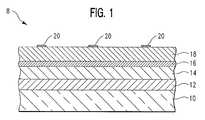
- the solar cell 8 is structurally supported on a glass substrate 10 having a thickness of approximately 1-4 mm.
- a back contact comprises a metal layer 12 of molybdenum having a thickness of approximately 0.2 microns deposited on substrate 10.
- the first semiconductor film 12 is p-type CIS having a thickness of approximately 1-3 microns having a thin layer 16 of chemically deposited insulating zinc oxide chemically deposited thereon from solution, as described below.
- the top layer is substantially conductive, transparent, CVD n-type zinc oxide having a thickness of 0.1- 3.0 microns.
- Front face contacts or patterning 20 are optionally deposited on the exposed surface of layer 18.
- ZnSo4 zinc sulfate
- NH4OH ammonium hydroxide
- Zn(OH)2 a precipitate of zinc hydroxide
- Further addition of ammonium hydroxide resulted in dissolution of the zinc hydroxide as a Zn/NH4 complex formed.
- Dipping small pieces of CIS substrates in the test tube batches of Zn/NH4 complex formed a layer of zinc hydroxide on their surfaces which, after optional drying with a stream of nitrogen, was then converted to zinc oxide through a dehydration step, by annealing the substrates in air at a temperature of approximately 2300 C for about 10 minutes.
- a third experiment comparing substrates dipped in solution concentrations of 0.01M ZnAC2/0.01M TEA/ 0.7M NH4OH for 1 min at 55C both with substrates dipped for 5 min at 55C and with a cadmium sulfide control produced cells with higher Voc than in the second experiment.
- the 1 min/55 C zinc oxide layer group had a best cell Voc of 495 mV.
- test substrate dipped at room temperature had a best cell Voc of 468 mV compared to 424 mV for the best cell dipped at 55°C.
- a further experiment compared the performance of cells dipped in solutions whose concentrations were selected from among those evaluated at a test tube scale. The results trend toward higher performance with increased concentration of all three chemicals.
- Cells dipped in 0.01M ZnAC2/0.01M TEA/ 0.64M NH4OH, and ZnAC2 and TEA at 1M and NH4OH at 1.4M produced higher efficiencies than CdS controls. This may be a practical limit on concentration of these three chemicals that can be used without forming free Zn(OH)2 precipitate in the bath.
- the CIS has been contacted with the solution by dipping in a bath thereof it is envisaged that, in an alternative approach the solution may be sprayed on the CIS.
- Figure 2 shows the Light IV curve for a 13.1% efficient cell formed from a dip concentration of 0.01M ZNAC2/0.OlM TEA/.7M NH4OH
Landscapes
- Photovoltaic Devices (AREA)
Abstract
Description
- The invention relates to thin film heterojunction solar cells formed from metal semiconductors, especially to those of the p-n type having a p-type layer comprising group I-III-VI semiconductors such as copper indium diselenide (CIS) and other chalcopyrite alloy materials and to a process for making high efficiency cells of such type.
- A known thin film, heterojunction solar cell of such type which was widely regarded as viable, is described in U.S.4,335,226, issued to Mickelsen et al on June 15, 1982 and teaches the provision of a layer of cadmium sulfide (CdS) on an absorber layer of CIS to provide a cell of high efficiency.
- Among the many documented attempts to improve such high efficiency cells are U.S. 4,611,091 issued to Choudray et al on September 9, 1986, and U.S. 5,045,409 issued to Eberspacher et al on September 3, 1991, the disclosures of which are incorporated by reference herein.
- The Eberspacher patent teaches an improved method of selenization of the CIS semiconductor, while Choudray teaches the replacement of a majority of the cadmium sulfide layer by providing a layer of a transparent, substantially conducting, wide band gap, n-type semiconductor, such as CVD zinc oxide, on only a very thin layer of chemically deposited cadmium sulfide.
- In essence, both the last two patents represent responses to the well recognized desirability of minimizing or eliminating the use of highly toxic materials such as hydrogen selenide and cadmium (sulfide) in large scale solar cell manufacturing processes.
- The chemically deposited cadmium sulfide approach taught by Choudary resulted in higher quality junctions than those from non-chemical, (non-cadmium) deposition processes in providing lower junction saturation current and increased shunt resistance such improvement believed to result from an etching and selective "cleaning" action on the heterojunction interface arising from the chemical dipping.
- An attempt to eliminate completely the highly toxic cadmium sulfide from the cell by replacement with zinc sulfide (Zns) deposited from a solution of zinc acetate (ZnAC₂) dissolved in ammonium hydroxide/ ammonium sulfide (NH4OH/(NH4)2S) was not successful. Although some zinc hydroxide (Zn(OH)₂), precipitate formed in the solution, no zinc could be detected on CIS dipped in that solution.
- However, the discovery some years later, of CIS modules with cadmium sulfide layers chemically deposited from solution having actual thicknesses of less than 10 A° but which, nevertheless, performed effectively, in spite of a belief that a minimum thickness of 100A° was necessary (in the Eberspacher cell), indicated that the cadmium sulfide was in fact acting substantially only as an insulating barrier between the CIS and CVD zinc oxide and that, possibly, relatively non-toxic, insulating zinc oxide, or other suitable metal oxides could perform the same function.
- An object of the invention is to provide a high efficiency, thin film, heterojunction solar cell of the above described type but which does not contain cadmium sulfide.
- A further object of the invention is to provide a process for making such solar cell which can be adapted for economical mass production at high volume while minimizing the concentrations or amounts of chemicals used while providing an acceptably high yield.
- An additional object of the invention is to provide a solar cell which provides improved open circuit voltage (Voc)
- According to one aspect of the invention, a thin film photovoltaic device comprises a metal back contact; a first multinary semiconductor film of a first conductivity type on said back contact, preferably comprising compound metals of group I-III-VI semiconductors, and other high gap chalcopyrite alloy materials; a second, transparent, metal semiconductor film of conductivity type opposite said first type on said first semiconductor film, and an interfacial film of a transparent, insulating metal oxide between said first semiconductor film and said second semiconductor film.
- More specifically, the second semiconductor film comprises zinc oxide, the first semiconductor film comprises copper indium diselenide (CIS) or alloy thereof and the insulating metal oxide comprises zinc oxide chemically deposited from solution thereon.
- According to another aspect, the invention comprises a process for making a photovoltaic device comprising the steps of depositing a first semiconductor metal film of a first conductivity type, preferably comprising one of group I-III-VI semiconductors, and other high gap chalcopyrite alloy materials on a metal back contact; chemically depositing from solution a film of a transparent, insulating metal oxide on said first semiconductor film; and depositing a second, transparent, semiconductor film of conductivity type opposite said first type on said first semiconductor film.
- More specifically, the film of transparent, insulating metal oxide is zinc oxide deposited by the steps of mixing one of zinc sulphate, zinc chloride and zinc acetate, preferably zinc acetate, with a suitable complexing agent such as ammonium hydroxide and, preferably triethanolamine (TEA) to dissolve the zinc salt and form a zinc/ammonium (Zn/NH₄) complex in solution; contacting, preferably by dipping, the first semiconductor film with the solution to deposit a thin film of zinc hydroxide from the solution on the first semiconductor film, and annealing the deposited zinc hydroxide film in air for a few minutes to dry and convert the insulating zinc hydroxide to zinc oxide. The zinc hydroxide deposit may be dried in a stream of nitrogen prior to the annealing step.
- Preferred solution concentrations are 0.01M ZnAC₂/0.01M TEA/ 0.64M NH₄OH; a dip time/temperature of 55°C/5 minutes and air annealing at 230⁰C for 10 minutes. A reduction of the concentrations of ZnAC₂ and TEA of up to 50% may still result in sufficient throughput speed with acceptable yields for practical manufacture, while an increase to 0.1M ZnAC₂/0.1M TEA/1.5M NH₄OH should provide somewhat higher yields through decreased reaction times. Further increases of ammonium hydroxide concentration to 3M are feasible while increases in concentrations of ZnAC₂ and TEA to 1M may be possible but the lower concentrations are desirable to avoid using more chemicals than necessary.
- Immersion times of between 1 and 5 minutes are effective in forming good cells on test substrates of CIS. Bath temperatures of 55C and about 20C both work well. For highest Voc, a 1 min/55C dip with solution concentrations of 0.01M ZnAC₂/0.01M TEA/ 0.7M NH₄OH is preferred while the highest efficiency is produced under the same operating conditions with a sulfidized CIS.
- Furthermore, 0.01M ZNAC₂/0.OlM TEA/.7M NH₄OH is preferred to 0.01M ZnSO₄/ 0.7M NH₄OH.
- Semiconductor materials of the first film layer may include CIS and other related I-III-VI terniary compunds and other multinary compounds such as cadmium telluride (CdTe). Insulating oxide layers, may include SnO₂, CdSnO₄, ZnSnO₄,In₂O₃.
-
- Figure 1 is a schematic cross sectional view of a type of solar cell according to the invention; and,
- Figure 2 is a Light IV, current/voltage, curve for a cell of the invention.
- The schematics of the solar cell structure are similar to that described in the above-mentioned patents and US 4,915,745 issued to Pollock on April 10, 1990, (reexamined and issued on April 7, 1992), the disclosure of which is incorporated herein by reference.
- As shown schematically in Figure 1 of the drawings, the
solar cell 8 is structurally supported on aglass substrate 10 having a thickness of approximately 1-4 mm. A back contact comprises ametal layer 12 of molybdenum having a thickness of approximately 0.2 microns deposited onsubstrate 10. Thefirst semiconductor film 12 is p-type CIS having a thickness of approximately 1-3 microns having athin layer 16 of chemically deposited insulating zinc oxide chemically deposited thereon from solution, as described below. The top layer is substantially conductive, transparent, CVD n-type zinc oxide having a thickness of 0.1- 3.0 microns. Front face contacts or patterning 20 are optionally deposited on the exposed surface oflayer 18. The techniques used in depositing such layers other thanlayer 16, together with a possible additional interfacial layer such comprising gallium (Ga) between the contact and the CIS, and the preferred methods of selenization of the CIS are described in the patents referred to above. - In initial developments on a test tube scale, zinc sulfate (ZnSo₄) solution was mixed with ammonium hydroxide (NH₄OH) and a precipitate of zinc hydroxide (Zn(OH)₂ formed. Further addition of ammonium hydroxide resulted in dissolution of the zinc hydroxide as a Zn/NH₄ complex formed. Dipping small pieces of CIS substrates in the test tube batches of Zn/NH₄ complex, formed a layer of zinc hydroxide on their surfaces which, after optional drying with a stream of nitrogen, was then converted to zinc oxide through a dehydration step, by annealing the substrates in air at a temperature of approximately 230⁰ C for about 10 minutes.
- Using Auger electron spectroscopy (AES) analysis, it was determine that ZnO was deposited on the substrates.
- Experiments also performed using zinc acetate (ZnAC₂) and triethanolamine(TEA) as an additional complexing agent led us to believe that, initially a solution of 0.01M ZnSO₄/O.7M NH₄OH and 55⁰C/5min dip time, then 0.01M ZnAC,/0.OlM TEA/0.7M NH₄OH showed suitable promise as chemical solutions for larger scale (Benchtop Dip) experiments.
- A subsequent series of benchtop scale experiments using 10x10cm CIS test substrates were performed.
- A first experiment comparing test substrates dipped in solution concentrations of 0.01M ZnSO₄/O.7M NH₄OH at 55⁰C for 10 minutes, both with substrates also predipped for 30 min in ammonium hydroxide and with a cadmium sulfide control made by the conventional process described in the above patents, indicated that using zinc sulfate as the zinc salt for forming the zinc oxide film could form a reasonably good junction on CIS in place of the cadmium sulfide dip control, the zinc oxide layer cells being almost as good as the cadmium sulfide controls. However, predipping the substrates in 0.35M ammonium hydroxide for 30 minutes was found to affect, negatively, the Voc (open circuit voltage) and FF (fill factor) of the cells, resulting in lower efficiencies for that group than either the non-predipped or cadmium sulfide control groups.
- A second experiment comparing substrates dipped in solution concentrations of 0.01M ZnAC₂/0.01M TEA/ 0.7M NH₄OH for 1 min at 55C with both dipping in only ammonium hydroxide solution and with a cadmium sulfide control demonstrated that cells made with ZnAC₂/TEA/NH₄OH performed better that the cadmium sulfide controls with higher Voc being the main improvement for the zinc oxide group. The best cell efficiency of any zinc oxide layer CIS cell produced in this experiment was 12.9% efficiency, 467 mV.
- A third experiment comparing substrates dipped in solution concentrations of 0.01M ZnAC₂/0.01M TEA/ 0.7M NH₄OH for 1 min at 55C both with substrates dipped for 5 min at 55C and with a cadmium sulfide control produced cells with higher Voc than in the second experiment. The 1 min/55 C zinc oxide layer group had a best cell Voc of 495 mV.
- A further experiment demonstrated that a 5 min dip at the last mentioned concentration using sulfidized CIS cells indicated that zinc oxide layer parts had higher efficiency and Voc than cadmium sulfide controls.
- As a result of a further experiment comparing the effect of dipping for 5 minutes with the solution at room temperature with a typical 55°C dip (only the temperature was varied), the test substrate dipped at room temperature had a best cell Voc of 468 mV compared to 424 mV for the best cell dipped at 55°C.
- However this was not confirmed by a subsequent experiment which indicated that the zinc oxide 55°C cell group was slightly better than the room temperature group and about comparable to a cadmium sulfide control. Possibly the results were affected by repeatedly using an old solution.
- A further experiment comparing the performance of TEA/NH₄OH only solution with that of the ZnO dip baseline conditions ( 0.01M ZNAC₂/0.OlM TEA/.64M NH₄OH) demonstrated that cells made without ZNAC₂ performed poorly indicating that the formation of the ZnO layer is necessary to good performance.
- We have also investigated the effect of the time and temperature of the dip process in two experiments, the first experiment over the temperature range of 25 - 55 C, with dip times between 1 and 10 minutes, indicated performance is improved by reducing the dip temperature. The performance peaked around 45 C and 5 minutes but the trend in time and temperature was not very strong. The performance was in general, better than CdS controls.
- However, the results of the second experiment in which the dip temperature was the main variable, were not confirmatory being, in general, lower and more scattered.
- We believe from these experiments that the temperature of the dip/ solution can be reduced below the baseline 55°C, but that the performance is not a strong function of the dip time or bath temperature.
- The effect of concentration of each of the chemicals, ZNAC., TEA and NH₄OH, in the ZnO dip bath was first explored by preparing small quantities in test tubes to observe the solution stability. The concentrations explored were the following:
ZnAC₂ and TEA - 0.001, 0.01 and 0.1M
NH₄OH - 1.4, 0.64 and 0.35M
It appeared that the formation kinetics for the Zn/NH₃ and Zn/TEA complexes are rather slow in reaching equilibrium as the solubility product for Zn(OH)₂ is approached. - A further experiment compared the performance of cells dipped in solutions whose concentrations were selected from among those evaluated at a test tube scale. The results trend toward higher performance with increased concentration of all three chemicals. Cells dipped in 0.01M ZnAC₂/0.01M TEA/ 0.64M NH₄OH, and ZnAC₂ and TEA at 1M and NH₄OH at 1.4M produced higher efficiencies than CdS controls. This may be a practical limit on concentration of these three chemicals that can be used without forming free Zn(OH)₂ precipitate in the bath.
- The parameters necessary to convert the ZN(OH)₂ layer deposited in the dip bath into zinc oxide were first studied using thermal analysis. Differential Scanning calorimetry of Zn(OH)₂ indicated that there were two transitions in the temperature range of 23 - 240°C, one at 100 C due to evaporation of H₂O and the other at around 140 C due to the decomposition of the hydroxide to oxide.
- Experiments to determine the results of annealing over the temperature range of 100 - 230°C for 5 - 15 minutes indicated that performance may peak around 180 C with the results varying as a function of time. At 100°C, performance trended downward with time but from 140 C up, the trend was toward better performance with increased time.
- Experiments using patterned substrates for enabling the effect of interconnects on performance to be evaluated by comparing the performance of baseline operating conditions with that of CdS controls using the minimodule test structure scheme designed by K. Knapp (10/25/90, Procedures for Fabricating Post-Module Test Structures), revealed no significant difference between the performance of ZnO dip and CdS control parts.
- Although the CIS has been contacted with the solution by dipping in a bath thereof it is envisaged that, in an alternative approach the solution may be sprayed on the CIS.
- Figure 2 shows the Light IV curve for a 13.1% efficient cell formed from a dip concentration of 0.01M ZNAC₂/0.OlM TEA/.7M NH₄OH
- It will be apparent from the foregoing that highly efficient and, in some respects better performing, cells are produced by substituting a chemically deposited, zinc oxide layer, for the prior cadmium sulfide layer thereby affording the opportunity of obviating the risks associated with using highly toxic materials such as cadmium.
Claims (18)
- A thin film photovoltaic device comprising a metal back contact; a first multinary semiconductor film of a first conductivity type on said back contact; a second, transparent, metal oxide semiconductor film of conductivity type opposite said first type on said first semiconductor film and a thin interfacial film of a transparent, insulating metal oxide between said first semiconductor film and said second semiconductor film.
- A photovoltaic device according to claim 1 in which the second semiconductor film comprises zinc oxide.
- A photovoltaic device according to claim 2 in which the insulating metal oxide comprises zinc oxide.
- A photovoltaic device according to claim 1 in which the first semiconductor film consists of one of copper indium diselenide and a group I-III-VI multinary compound.
- A photovoltaic device according to claim 3 in which the first semiconductor film comprises copper indium diselenide.
- A process for making a thin film heterojunction photovoltaic device comprising the steps of:
depositing a first multinary semiconductor film of a first conductivity type on a metal back contact;
chemically depositing from solution a thin film of a transparent, insulating metal oxide on said first semiconductor film; and
depositing a second, transparent metal oxide semiconductor film of conductivity type opposite said first type on said first semiconductor film. - A process according to claim 6 in which the film of transparent, insulating metal oxide is deposited by the steps of:
mixing a zinc salt with a suitable complexing agent to dissolve the zinc salt and form a zinc/ammonium (Zn/NH₄) complex in solution;
contacting, the first compound semiconductor film with the solution to deposit a thin film of zinc hydroxide from the solution on the first compound semiconductor film;
annealing the deposited zinc hydroxide film to convert the insulating zinc hydroxide to zinc oxide. - A process according to claim 6 in which the second semiconductor film is n-type zinc oxide.
- A process according to claim 8 in which the first semiconductor film comprises copper indium diselenide.
- A process according to claim 8 in which the zinc salt is one of zinc sulphate, zinc chloride and zinc acetate.
- A process according to claim 10 wherein the complexing agent comprises ammonium hydroxide.
- A process according to claim 11 wherein the zinc salt is zinc acetate and the complexing agent further comprises triethanolamine.
- A process according to claim 12 wherein the solution comprises 0. 001M to 0.1M zinc salt dissolved in 0.001M to 1.5M ammonium hydroxide.
- A process according to claim 13 wherein the solution comprises 0.01M to 0.1M zinc salt dissolved in 0.1M to 1.5M ammonium hydroxide.
- A process according to claim 14 wherein the solution comprises approximately 0. 01M zinc salt dissolved in approximately 0.7M ammonium hydroxide.
- A process according to claim 11 wherein the zinc salt is zinc sulfate.
- A process according to claim 12 wherein the solution comprises 0.01M to 0.1M zinc acetate, 0.01M to 0.1M TEA and 0.6M to 1.5M ammonium hydroxide.
- A process according to claim 17 wherein the solution comprises approximately 0.01M zinc acetate, 0.01M TEA and 0.64M ammonium hydroxide.
Applications Claiming Priority (2)
| Application Number | Priority Date | Filing Date | Title |
|---|---|---|---|
| US99821192A | 1992-12-30 | 1992-12-30 | |
| US998211 | 1992-12-30 |
Publications (3)
| Publication Number | Publication Date |
|---|---|
| EP0604801A2 true EP0604801A2 (en) | 1994-07-06 |
| EP0604801A3 EP0604801A3 (en) | 1994-11-23 |
| EP0604801B1 EP0604801B1 (en) | 1999-10-06 |
Family
ID=25544924
Family Applications (1)
| Application Number | Title | Priority Date | Filing Date |
|---|---|---|---|
| EP93119798A Expired - Lifetime EP0604801B1 (en) | 1992-12-30 | 1993-12-08 | Method of making a thin film heterojunction solar cell |
Country Status (3)
| Country | Link |
|---|---|
| EP (1) | EP0604801B1 (en) |
| JP (1) | JPH077167A (en) |
| DE (1) | DE69326676T2 (en) |
Cited By (2)
| Publication number | Priority date | Publication date | Assignee | Title |
|---|---|---|---|---|
| DE4440878A1 (en) * | 1994-11-16 | 1996-07-18 | Zsw | Cpd. semiconductor thin film solar cell |
| WO2007071663A1 (en) * | 2005-12-21 | 2007-06-28 | Shell Erneuerbare Energien Gmbh | Process of making a thin-film photovoltaic device and thin-film photovoltaic device |
Families Citing this family (2)
| Publication number | Priority date | Publication date | Assignee | Title |
|---|---|---|---|---|
| JP3249407B2 (en) * | 1996-10-25 | 2002-01-21 | 昭和シェル石油株式会社 | Thin-film solar cells composed of chalcopyrite-based multi-compound semiconductor thin-film light-absorbing layers |
| KR101181095B1 (en) * | 2010-10-11 | 2012-09-07 | 엘지이노텍 주식회사 | Solar cell and method for manufacturing the same |
Family Cites Families (1)
| Publication number | Priority date | Publication date | Assignee | Title |
|---|---|---|---|---|
| US4612411A (en) * | 1985-06-04 | 1986-09-16 | Atlantic Richfield Company | Thin film solar cell with ZnO window layer |
-
1993
- 1993-12-08 EP EP93119798A patent/EP0604801B1/en not_active Expired - Lifetime
- 1993-12-08 DE DE69326676T patent/DE69326676T2/en not_active Expired - Lifetime
- 1993-12-27 JP JP5332546A patent/JPH077167A/en active Pending
Cited By (7)
| Publication number | Priority date | Publication date | Assignee | Title |
|---|---|---|---|---|
| DE4440878A1 (en) * | 1994-11-16 | 1996-07-18 | Zsw | Cpd. semiconductor thin film solar cell |
| DE4440878C2 (en) * | 1994-11-16 | 1999-04-29 | Zsw | Compound semiconductor thin-film solar cell and process for its production |
| DE4447865B4 (en) * | 1994-11-16 | 2006-06-14 | Zentrum für Sonnenenergie- und Wasserstoff-Forschung Baden-Württemberg | Compound semiconductor thin film solar cell with alkali metal addition and method of preparation |
| WO2007071663A1 (en) * | 2005-12-21 | 2007-06-28 | Shell Erneuerbare Energien Gmbh | Process of making a thin-film photovoltaic device and thin-film photovoltaic device |
| CN101346823B (en) * | 2005-12-21 | 2010-06-23 | 壳牌可再生能源有限公司 | Method for producing thin-film photovoltaic device and thin-film photovoltaic device |
| EP2239782A1 (en) | 2005-12-21 | 2010-10-13 | Saint-Gobain Glass France | Thin-Film photovoltaic device |
| US8673678B2 (en) | 2005-12-21 | 2014-03-18 | Saint-Gobain Glass France | Process of making a thin-film photovoltaic device and thin-film photovoltaic device |
Also Published As
| Publication number | Publication date |
|---|---|
| EP0604801B1 (en) | 1999-10-06 |
| DE69326676T2 (en) | 2000-03-09 |
| DE69326676D1 (en) | 1999-11-11 |
| JPH077167A (en) | 1995-01-10 |
| EP0604801A3 (en) | 1994-11-23 |
Similar Documents
| Publication | Publication Date | Title |
|---|---|---|
| US5474939A (en) | Method of making thin film heterojunction solar cell | |
| Chu et al. | Thin film II–VI photovoltaics | |
| Kapadnis et al. | Cadmium telluride/cadmium sulfide thin films solar cells: a review | |
| US4950615A (en) | Method and making group IIB metal - telluride films and solar cells | |
| Chu et al. | Recent progress in thin‐film cadmium telluride solar cells | |
| Kemell et al. | Thin film deposition methods for CuInSe 2 solar cells | |
| KR100355822B1 (en) | Semiconductor thin film, method of manufacturing the same, and solar cell using the same | |
| US20050257825A1 (en) | Zno/cu(inga)se2 solar cells prepared by vapor phase zn doping | |
| JP3249342B2 (en) | Heterojunction thin-film solar cell and method of manufacturing the same | |
| Kushiya et al. | Application of Zn-Compound Buffer Layer for Polycrystalline C u I n S e 2-Based Thin-Film Solar Cells | |
| EP0956600A1 (en) | PREPARATION OF Cu x?In y?Ga z?Se n? (x=0-2, y=0-2, z=0-2, n=0-3) PRECURSOR FILMS BY ELECTRODEPOSITION FOR FABRICATING HIGH EFFICIENCY SOLAR CELLS | |
| Saha | A Status Review on Cu2ZnSn (S, Se) 4‐Based Thin‐Film Solar Cells | |
| Garg et al. | Characterization of p-CuInSe2 films for photovoltaics grown by a chemical deposition technique | |
| Huse et al. | Characterization of economic and non-toxic copper doped zinc sulfide thin film grown by facile chemical bath deposition method | |
| US7611573B2 (en) | ZnS/Zn(O,OH)S-based buffer layer deposition for solar cells | |
| WO2015120512A1 (en) | A photovoltaic cell and a method of forming a photovoltaic cell | |
| EP0604801B1 (en) | Method of making a thin film heterojunction solar cell | |
| Bayhan et al. | Eects of Post Deposition Treatments on Vacuum Evaporated CdTe Thin Films and CdS= CdTe Heterojunction Devices | |
| KR101081300B1 (en) | Solar cell and method of fabricating the same | |
| Prawira et al. | All-solution-non-vacuum fabrication process of CZTS solar cell using ZTO as non-toxic buffer layer | |
| Gal et al. | Engineering the interface energetics of solar cells by grafting molecular properties onto semiconductors | |
| Abdullah et al. | A Review on Development Prospect of CMTS Based Thin Film Solar Cells | |
| Chu et al. | High efficiency thin film cadmium telluride solar cells | |
| Liyanage | Improving Performance in Cadmium Telluride Solar Cells: From Fabrication to Understanding the Pathway Towards 25% Efficiency | |
| Reddy et al. | Thin films of tin sulphide for application in photovoltaic solar cells |
Legal Events
| Date | Code | Title | Description |
|---|---|---|---|
| PUAI | Public reference made under article 153(3) epc to a published international application that has entered the european phase |
Free format text: ORIGINAL CODE: 0009012 |
|
| AK | Designated contracting states |
Kind code of ref document: A2 Designated state(s): DE FR GB IT |
|
| PUAL | Search report despatched |
Free format text: ORIGINAL CODE: 0009013 |
|
| AK | Designated contracting states |
Kind code of ref document: A3 Designated state(s): DE FR GB IT |
|
| 17P | Request for examination filed |
Effective date: 19950518 |
|
| 17Q | First examination report despatched |
Effective date: 19960124 |
|
| GRAG | Despatch of communication of intention to grant |
Free format text: ORIGINAL CODE: EPIDOS AGRA |
|
| GRAG | Despatch of communication of intention to grant |
Free format text: ORIGINAL CODE: EPIDOS AGRA |
|
| GRAH | Despatch of communication of intention to grant a patent |
Free format text: ORIGINAL CODE: EPIDOS IGRA |
|
| GRAH | Despatch of communication of intention to grant a patent |
Free format text: ORIGINAL CODE: EPIDOS IGRA |
|
| GRAA | (expected) grant |
Free format text: ORIGINAL CODE: 0009210 |
|
| AK | Designated contracting states |
Kind code of ref document: B1 Designated state(s): DE FR GB IT |
|
| REF | Corresponds to: |
Ref document number: 69326676 Country of ref document: DE Date of ref document: 19991111 |
|
| ITF | It: translation for a ep patent filed | ||
| ET | Fr: translation filed | ||
| PLBE | No opposition filed within time limit |
Free format text: ORIGINAL CODE: 0009261 |
|
| STAA | Information on the status of an ep patent application or granted ep patent |
Free format text: STATUS: NO OPPOSITION FILED WITHIN TIME LIMIT |
|
| 26N | No opposition filed | ||
| REG | Reference to a national code |
Ref country code: GB Ref legal event code: IF02 |
|
| REG | Reference to a national code |
Ref country code: FR Ref legal event code: CD |
|
| REG | Reference to a national code |
Ref country code: FR Ref legal event code: TP |
|
| PG25 | Lapsed in a contracting state [announced via postgrant information from national office to epo] |
Ref country code: IT Free format text: LAPSE BECAUSE OF NON-PAYMENT OF DUE FEES Effective date: 20091208 |
|
| PGRI | Patent reinstated in contracting state [announced from national office to epo] |
Ref country code: IT Effective date: 20110616 |
|
| PGFP | Annual fee paid to national office [announced via postgrant information from national office to epo] |
Ref country code: DE Payment date: 20121205 Year of fee payment: 20 |
|
| PGFP | Annual fee paid to national office [announced via postgrant information from national office to epo] |
Ref country code: IT Payment date: 20121213 Year of fee payment: 20 Ref country code: GB Payment date: 20121205 Year of fee payment: 20 |
|
| PGFP | Annual fee paid to national office [announced via postgrant information from national office to epo] |
Ref country code: FR Payment date: 20130107 Year of fee payment: 20 |
|
| REG | Reference to a national code |
Ref country code: DE Ref legal event code: R082 Ref document number: 69326676 Country of ref document: DE Representative=s name: SPLANEMANN PATENTANWAELTE PARTNERSCHAFT, DE |
|
| REG | Reference to a national code |
Ref country code: DE Ref legal event code: R071 Ref document number: 69326676 Country of ref document: DE |
|
| REG | Reference to a national code |
Ref country code: GB Ref legal event code: PE20 Expiry date: 20131207 |
|
| PG25 | Lapsed in a contracting state [announced via postgrant information from national office to epo] |
Ref country code: DE Free format text: LAPSE BECAUSE OF EXPIRATION OF PROTECTION Effective date: 20131210 Ref country code: GB Free format text: LAPSE BECAUSE OF EXPIRATION OF PROTECTION Effective date: 20131207 |