EP0601201B1 - Waveform a/d converter and d/a converter - Google Patents
Waveform a/d converter and d/a converter Download PDFInfo
- Publication number
- EP0601201B1 EP0601201B1 EP93913522A EP93913522A EP0601201B1 EP 0601201 B1 EP0601201 B1 EP 0601201B1 EP 93913522 A EP93913522 A EP 93913522A EP 93913522 A EP93913522 A EP 93913522A EP 0601201 B1 EP0601201 B1 EP 0601201B1
- Authority
- EP
- European Patent Office
- Prior art keywords
- waveform
- converter
- differential
- converting
- digital
- Prior art date
- Legal status (The legal status is an assumption and is not a legal conclusion. Google has not performed a legal analysis and makes no representation as to the accuracy of the status listed.)
- Expired - Lifetime
Links
Images


Classifications
-
- H—ELECTRICITY
- H03—ELECTRONIC CIRCUITRY
- H03M—CODING; DECODING; CODE CONVERSION IN GENERAL
- H03M3/00—Conversion of analogue values to or from differential modulation
-
- G—PHYSICS
- G06—COMPUTING; CALCULATING OR COUNTING
- G06J—HYBRID COMPUTING ARRANGEMENTS
- G06J1/00—Hybrid computing arrangements
Definitions
- the present invention relates to an A/D converter and a D/A converter for converting an analog or digital waveform signal to digital or analog waveform signal and, more particularly, to an A/D converter and a D/A converter which implement high-speed, high-resolution waveform conversion through use of a plurality of A/D or D/A conversion parts.
- JP-A-57-140026 discloses a D/A converter wherein an input digital signal is input to a digital adder, the output of which is supplied to an inverter.
- a cascade connection consisting of several delay elements is connected to the output of the inverter, with each output of each delay element being supplied to the digital adder.
- the output of the digital adder thus forms a sum of three differential waveforms (after an initial transient phase of ca 10 sample periods) which is fed, via a distribution switch, to registers sequentially and circulatingly.
- the output of each register is connected to a D/A converter generating analog values which are added by means of a further adder generating the final analog output signal corresponding to the input digital signal.
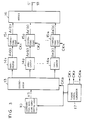
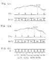
- Fig. 1A is a block diagram of the A/D converter of the above-mentioned prior art example, in which plural (for example, two) A/D converting parts AD 1 and AD 2 are connected in parallel to and are driven alternately with each other to thereby implement an A/D converter of an operating speed twice higher than that of a single A/D converting part.
- the A/D converting parts AD 1 and AD 2 have their inputs connected in parallel to each other and alternately convert the amplitude of the input analog waveforms S A to digital values D 1 and D 2 at the timing of their clocks CK 1 and CK 2 as shown in Fig. 1B and hold the converted value until the occurrence of the next clock.
- a multiplexer 2 responds to the clocks CK 1 and CK 2 to output the digital values D 1 and D 2 alternately with each other, providing a digital waveform S D .
- the digital waveform S D is composed of outputs a n and b n that are provided alternately from the A/D converting parts AD 1 and AD 2 ; thus, the A/D converter outputs data at an operating speed twice higher than that of the individual A/D converting parts AD 1 and AD 2 .
- Fig. 2A is a diagram showing a digital data waveform distorted by the gain error; the gain error between the two A/D converting parts is 10% in this example.
- Fig. 2B is a diagram showing a digital data waveform distorted by the offset error; the offset error between the two converting parts is 10% in this example. In either of Figs.
- a D/A converter for waveform conversion also encounters similar problems. That is, by distributing an input digital waveform signal to a plurality of D/A converting parts one after another through a multiplexer for conversion into analog signals and then switching the converted outputs one after another through a switch to output an analog waveform signal, the operating speed for the D/A conversion can be increased, but the output waveform is distorted by a gain error and an offset error between the plurality of D/A converting parts and the resolution of the output anaiog waveform is not improved. Also in this instance, if the output changeover switch is replaced with an analog adder, the gain and offset errors between the respective D/A converting parts are averaged, and consequently, the distortion by these errors is reduced but the resolution still remains unimproved.
- to add the outputs from a plurality of converting parts in the A/D or D/A converting device is to average the amplitude of a waveform at a plurality of successive sample points -- this only makes the waveform gentle by applying the waveform signal to a low-pass filter and does not improve resolution.
- An object of the present invention is to provide an A/D converter (or D/A converter) for waveform conversion which permits high-speed, high-resolution waveform conversion through use of a plurality of A/D (or D/A) converting parts and reduces the distortion of the converted output waveform that is attributable to the gain and offset errors between the converting parts.
- the present invention provides an A/D converter and D/A converter in accordance with claim 1 and 2, respectively.
- each converting means needs only to convert every N-th one of differential waveforms that are distributed from the distributing means -- this permits high-speed conversion throughout the N converting means.
- the output from the adding means represents the amplitude itself at each sample point of the input waveform, i.e. the waveform before conversion, not the average value of the waveform.
- resolution at the output of the adding means is increased N times higher than the resolution of the individual converting means.
- the gain and offset errors between the converting means are averaged down to 1/N.
- Fig. 1A is a block diagram showing an example of a conventional A/D converter adapted for high-speed operation through use of a plurality of A/D converting parts.
- Fig. 1B is a timing chart for explaining the operation of the A/D converter shown in Fig. 1A.
- Fig. 2A is a diagram showing an output digital waveform from the A/D converter of Fig. 1A which contains distortion attributable to a 10% gain error.
- Fig. 2B is a diagram showing an output digital waveform from the A/D converter of Fig. 1A which contains distortion attributable to a 10% offset error.
- Fig. 3 is a block diagram illustrating the basic construction of the A/D converter and the D/A converter for waveform conversion according to the present invention.
- Fig. 4 is a waveform diagram for explaining the operation of the converters depicted in Fig. 3.
- Fig. 5A is a block diagram illustrating an embodiment of the A/D converter according to the present invention.
- Fig. 5B is a timing chart showing the operation of the A/D converter depicted in Fig. 5A.
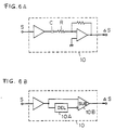
- Fig. 6A is a diagram illustrating an embodiment of an analog differentiation circuit 10.
- Fig. 6B is a diagram illustrating another embodiment of the analog differentiation circuit 10.
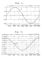
- Fig. 7A is a diagram showing an analog input waveform to the differentiation circuit 10.
- Fig. 7B is a diagram showing the output waveform from the differentiation circuit 10 which has differentiated the analog input waveform.
- Fig. 8A is a diagram showing one of two output waveforms distributed by a distributor 13.
- Fig. 8B is a diagram showing the other output waveform distributed by the distributor 13.
- Fig. 9A is a diagram showing the output waveform from the one integrator 14 1 .
- Fig. 9B is a diagram showing the output waveform from the other integrator 14 2 .
- Fig. 10A is a diagram for explaining how to control the timing for A/D conversion in the one A/D converting part AD 1 .
- Fig. 10B is a diagram for explaining how to control the timing for A/D conversion in the other A/D converting part AD 2 .
- Fig. 10C is a diagram showing the output digital waveform data from an adder 16.
- Fig. 11 is a diagram showing the output digital waveform from the adder in the case where no error is present between the A/D converting parts AD 1 and AD 2 .
- Fig. 12 is a diagram showing the output digital waveform from the adder in the case where a 10% gain error is present between the converting parts AD 1 and AD 2 .
- Fig. 13 is a diagram showing the output digital waveform from the adder in the case where a 10% offset error is present between the converting parts AD 1 and AD 2 .
- Fig. 14 is a block diagram illustrating an embodiment of the present invention of Fig. 3 applied to a D/A converter.
- Fig. 15 is a diagram for explaining the D/A converting operation of the Fig. 14 embodiment.
- Fig. 16 is a diagram showing an example of the D/A converted output waveform of the Fig. 14 embodiment.
- Fig. 17 is a block diagram illustrating a modified form of the Fig. 14 embodiment in which a differential waveform generating part 10 is formed by a waveform memory having stored therein differential waveforms.
- Fig. 18 is a block diagram illustrating an embodiment in which outputs from integrators 14 1 through 14 4 in Fig. 14 are prestored in separate waveform memories.
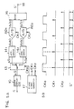
- Fig. 3 is a theoretical block diagram showing either of the A/D converter and the D/A converter according to the present invention. That is, in the case where a differential waveform ⁇ S that is output from a differential waveform generating part 10 is an analog signal, converting parts 15 1 through 15 N are all A/D converting parts, and when the differential waveform ⁇ S is a digital signal, the converting parts 15 1 through 15 N are D/A converting parts.
- the differential value ⁇ S of the waveform is fed from the differential waveform generating part 10 to a distributor 13.
- the distributor 13 repeats distributing the differential value ⁇ S to the N (where N is an integer equal to or greater than 2) integrators 14 1 through 14 N one after another in synchronization with a clock signal CK 0 from a timing signal generator 17.
- the integrators 14 1 through 14 N integrate the differential values distributed thereto and the integrated outputs are A/D or D/A converted by the converting parts 15 1 through 15 N at the timing of clock signals CK 1 through CK N .
- Converted outputs A 1 '(t) through A N '(t) from the converting parts 15 1 through 15 N are provided to and added together by an adder 16, and a converted output waveform S' is obtained at a terminal 18.
- Fig. 4 shows waveforms that occur at respective parts of the A/D or D/A converter, for explaining the principle of operation thereof.
- An analog waveform signal S is applied to the differential waveform generating part 10, from which variations ⁇ S(1), ⁇ S(2), ⁇ S(3), ... of the input waveform signal every clock CK 0 are sequentially output as the differential waveform ⁇ S.
- the distributor 13 distributes these variations to the integrators 14 1 through 14 N in a sequential order.
- the integrator 14 1 is supplied with the variations ⁇ S(1), ⁇ S(N+1), ⁇ S(2N+1), ... at time intervals ⁇ tN and integrates them.
- the resulting integrated output A 1 (t) varies stepwise as shown.
- the integrated output A 1 (t) is A/D converted by the A/D converting part 15 1 and the converted output A 1 '(t) is fed to the adder 16.
- Similar processing is also carried out by corresponding combinations of the integrators 14 2 through 14 N and converting parts 15 2 through 15 N , and the adder 16 adds together the converted signals A 1 '(t) through A N '(t) and provides the added output as the converted digital signal S'.
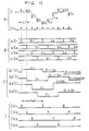
- Fig. 5A is a block diagram of the converter of the present invention applied to an A/D converter, which employs two A/D converting parts AD 1 and AD 2 .
- Fig. 5B is a timing chart for explaining the operation of the A/D converter shown in Fig. 5A.
- the differential waveform generating part 10 is formed by a differentiator which differentiates the analog input waveform S to obtain its variations.
- the distributor 13 is a high-speed electronic switch, which responds to the clock CK 0 to output the differential output waveform ⁇ S to the integrators 14 1 and 14 2 alternately with each other.
- the integrators 14 1 and 14 2 integrate the differential output waveforms ⁇ S 1 and ⁇ S 2 that are distributed from the distributor 13.
- the A/D converting parts AD 1 and AD 2 convert the integrated outputs from the integrators 14 1 and 14 2 to digital values, respectively.
- the adder 16 adds together the output digital values from the A/D converting parts AD 1 and AD 2 and outputs the digital waveform S'.
- the differentiation circuit 10 may be formed by a known primary high-pass filter using a capacitor C and a resistor R, for example, as shown in Fig. 6A. It is also possible to employ such a circuit construction as shown in Fig. 6B, in which the input analog waveform signal S is applied to the one input of a subtractor 10B and a waveform signal S delayed by a delay element 10A for a predetermined period of time is applied to the other input of the subtractor and the difference between these two signals is obtained as the differential output ⁇ S. It will easily be understood by those skilled in the art that various other differentiation circuits can be used.
- the output ⁇ S from the differentiation circuit 10 becomes such a cosine-wave signal as shown in Fig. 7B.
- Distributing the cosine-wave signal ⁇ S by the distributor 13 into two series, signals ⁇ S 1 and ⁇ S 2 depicted in Figs. 8A and 8B are obtained.
- the distributor 13 is formed by a high-speed electronic switch, whose connection is changed over in accordance with the control clock CK 0 from the timing signal generating part 17, such as shown in Fig. 5B.
- the distributed output waveform ⁇ S 1 shown in Fig. 8A, is fed to and integrated by the integrator 14 1 .
- Fig. 9A shows the output waveform A 1 (t) from the integrator 14 1 . That is, upon each occurrence of a substantially strip-like input, it is integrated by the integrator 14 1 and its output waveform A 1 (t) increases or decreases. In respective sections where no such strip-shaped input is present, the output waveform A 1 (t) from the integrator 14 1 maintains the level immediately preceding the section.
- the distributed output waveform ⁇ S 2 shown in Fig. 8B is provided to and integrated by the integrator 142, from which is obtained the integrated output waveform A 2 (t) depicted in Fig. 9B.
- the output waveforms A 1 (t) and A 2 (t) shown in Figs. 9A and 9B are fed to the A/D converting parts AD 1 and AD 2 , respectively.
- the A/D converting parts AD 1 and AD 2 convert the integrated outputs A 1 (t) and A 2 (t) into a sequence A 1 '(t) of digital values a 1 , a 2 , a 3 , ... and a sequence A 2 '(t) of digital values b 1 , b 2 , b 3 , ... at the timing of the clock signals CK 1 and CK 2 from the timing signal generating part 17, respectively.
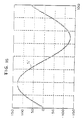
- Fig. 10C shows a data sequence of the digital waveform S' obtained by adding together the digital outputs A 1 '(t) and A 2 '(t) from the A/D converting parts AD 1 and AD 2 in the adder 16, and the added digital waveform is such as shown in Fig. 11, for instance. Incidentally, this is the case where no gain and offset errors exist between the A/D converting parts AD 1 and AD 2 .
- Fig. 12 shows an example of the output digital waveform S' provided from the adder 16 when a 10% gain error exists between the two A/D converting parts AD 1 and AD 2 ; in this case, the waveform contains a total of about 5% gain error but its distortion is small.
- Fig. 13 shows an example of the output digital waveform from the adder in the case where a 10% offset error exists between the two A/D converting parts AD 1 and AD 2 ; in this instance, the waveform contains a total of about 5% offset error but its distortion is small.
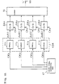
- Fig. 14 illustrates an embodiment of the Fig. 3 construction of the invention applied to a D/A converter for waveform conversion, in which the number of distributed outputs, N, by the distributor 13 is 4.
- the input digital waveform signal S may be provided from the outside, but in this embodiment, the differential waveform generating part 10 is formed by a waveform memory 11 and a differentiation circuit 12 and the digital waveform S prestored in the waveform memory 11 is read out therefrom in synchronization with the clock CK 0 and fed to the differentiation circuit 12.
- the differentiation circuit 12 outputs, as the digital differential waveform value ⁇ S, a difference (i.e. a variation) of the input digital waveform data S upon each occurrence of the clock CK 0 , for instance.
- the digital differential waveform ⁇ S thus generated by the differentiation circuit 12 is fed to the distributor 13, from which it is distributed to the digital integrators 14 1 through 14 4 one after another in synchronization with the clock CK 0 .
- the digital integrated outputs A 1 (t) through A 4 (t) from the integrators 14 1 through 14 4 are applied to D/A converting parts DA 1 through DA 4 , whereby they are converted to analog signals A 1 '(t) through A 4 '(t) upon occurrence of clock signals CK 1 through CK 4 , respectively.
- the outputs A 1 '(t) through A 4 '(t) from the D/A converting parts DA 1 through DA 4 are applied to and added together by an analog adder 16 and output therefrom as an analog waveform signal S'.
- Fig. 15A shows the digital waveform S read out from the waveform memory 11 and the arrows a 1 , b 1 , c 1 , d 1 , a 2 , b 2 , c 2 , d 2 , a 3 , b 3 , ... on the waveform represent the outputs ⁇ S from the differentiation circuit 12 that has differentiated the waveform S at the timing of the clock CK 0 , the arrows also representing the signs of the differentiated outputs. As shown in Fig.
- Fig. 15C shows the outputs A 1 '(t) through A 4 '(t) in the case where the pieces of differentiated data ⁇ S 1 through ⁇ S 4 input into the integrators 14 1 through 14 4 were accumulated at the timing of clock signals CK 1 through CK 4 shown in Fig. 15D and the integrator outputs were converted by the D/A converting parts DA 1 through DA 4 into digital form.
- the D/A converting parts DA 1 through DA 4 perform conversion at time intervals 4 ⁇ t four times longer than the cycle of the clock signal CK 0 and in phases displaced apart in steps of the clock cycle ⁇ t, as shown in Fig. 15D.
- the analog signals A 1 '(t) through A 4 '(t) sequentially converted by the four D/A converting parts DA 1 through DA 4 are added together by the analog adder 16, from which is obtained the analog waveform S' shown in Fig. 15A.
- Fig. 16 shows an example of the analog waveform that is provided from the analog adder 16 when digital sinusoidal waveform data is read out from the waveform data memory 11.
- the maximum amplitude of the analog waveform signal S' obtained by adding the four analog signals A 1 '(t) through A 4 '(t) by the adder 16, becomes the sum of maximum amplitudes of the outputs from the respective D/A converting parts; hence, resolution is improved four times higher than the resolution obtainable with a single D/A converting part, while at the same time the gain error and the offset error between the D/A converting parts DA 1 through DA 4 are respectively reduced down to 1/4.
- the converting operation speed of the D/A converter in its entirety becomes four times higher than the operating speed of each D/A converting part.
- the positions of the integrators 14 1 through 14 4 and the D/A converting parts DA 1 through DA 4 may be reversed in the Fig. 14 embodiment. That is, the pieces of data sequentially distributed by the distributor 13 are first converted by the D/A converting parts DA 1 through DA 4 to analog form, the analog differentiated waveforms thus obtained are integrated by the integrators 14 1 through 14 4 and then added by the analog adder 16.
- the differential waveform generating part 10 needs only to output the differential waveform data ⁇ S
- the differentiation circuit 12 is unnecessary and the output of the memory 11 is connected to the distributor 13.
- the output data A 1 (t) through A 4 (t) from the integrators 14 1 through 14 4 with respect to a desired waveform in the embodiment of Fig. 14 are precalculated and prestored in four waveform data memories 11 1 through 11 4 , respectively, as shown in Fig. 18, the distributor 13 and the integrators 14 1 through 144 as well as the differentiation circuit 12 will become unnecessary.
- the pieces of data individually stored in the waveform data memories 11 1 through 11 4 are read out therefrom in a sequential order at the timing of the clock signals CK 1 through CK 4 and are D/A converted by the corresponding D/A converting parts DA 1 through DA 4 , and then the converted outputs are added together in the analog adder 16.
Description
- The present invention relates to an A/D converter and a D/A converter for converting an analog or digital waveform signal to digital or analog waveform signal and, more particularly, to an A/D converter and a D/A converter which implement high-speed, high-resolution waveform conversion through use of a plurality of A/D or D/A conversion parts.
- JP-A-57-140026 (Abstract) discloses a D/A converter wherein an input digital signal is input to a digital adder, the output of which is supplied to an inverter. A cascade connection consisting of several delay elements is connected to the output of the inverter, with each output of each delay element being supplied to the digital adder. The output of the digital adder thus forms a sum of three differential waveforms (after an initial transient phase of ca 10 sample periods) which is fed, via a distribution switch, to registers sequentially and circulatingly. The output of each register is connected to a D/A converter generating analog values which are added by means of a further adder generating the final analog output signal corresponding to the input digital signal.
- In general, high resolution and high-speed operations are required to convert an analog or digital waveform to a digital or analog signal with high precision. However, high-speed, high-resolution A/D and D/A converters are very expensive. Hence, it is customary in the prior art to implement a converter whose conversion rate, as a whole, is made N-fold by applying waveform signals to a plurality (N) of low-speed, high-resolution converting parts, converting the signals one after another at a fixed time interval while shifting their phases by a time T/N, and outputting the converted versions one after another from the converting parts in a circulating fashion. A description will be given, with reference to Figs. 1A and 1B, of the case of implementing an A/D converter, for instance.
- Fig. 1A is a block diagram of the A/D converter of the above-mentioned prior art example, in which plural (for example, two) A/D converting parts AD1 and AD2 are connected in parallel to and are driven alternately with each other to thereby implement an A/D converter of an operating speed twice higher than that of a single A/D converting part. The A/D converting parts AD1 and AD2 have their inputs connected in parallel to each other and alternately convert the amplitude of the input analog waveforms SA to digital values D1 and D2 at the timing of their clocks CK1 and CK2 as shown in Fig. 1B and hold the converted value until the occurrence of the next clock.
- A
multiplexer 2 responds to the clocks CK1 and CK2 to output the digital values D1 and D2 alternately with each other, providing a digital waveform SD. As shown in Fig. 1B, the digital waveform SD is composed of outputs an and bn that are provided alternately from the A/D converting parts AD1 and AD2; thus, the A/D converter outputs data at an operating speed twice higher than that of the individual A/D converting parts AD1 and AD2. - In the above-described A/D converter wherein a plurality of A/D converting parts are connected in parallel and are sequentially activated, for example, in the case of Fig. 1A, a gain error and an offset error that inevitably exist between the A/D converting parts AD1 and AD2 will distort the waveform as depicted in Figs. 2A and 2B. Fig. 2A is a diagram showing a digital data waveform distorted by the gain error; the gain error between the two A/D converting parts is 10% in this example. Fig. 2B is a diagram showing a digital data waveform distorted by the offset error; the offset error between the two converting parts is 10% in this example. In either of Figs. 2A and 2B, the error appears between all adjacent pieces of data in the output of the
multiplexer 2. Furthermore, since the output from themultiplexer 2 only switches between the outputs from the A/D converting parts AD1 and AD2 alternately, the resolution of the output value is the same as that of the individual A/D converting parts AD1 and AD2. That is, the construction of Fig. 1A permits the speeding up of the A/D converting operation but fails to improve the resolution of the converted output SD. In Fig. 1A, by providing an adder in place of themultiplexer 2 and outputting therefrom the sums of adjacent pieces of data, a1+b1, b1+a2, a2+b3, b3+a4, ..., the distortion by the error between the A/D converting parts AD1 and AD2 is averaged and hence is improved, but the resolution is not improved. - A D/A converter for waveform conversion also encounters similar problems. That is, by distributing an input digital waveform signal to a plurality of D/A converting parts one after another through a multiplexer for conversion into analog signals and then switching the converted outputs one after another through a switch to output an analog waveform signal, the operating speed for the D/A conversion can be increased, but the output waveform is distorted by a gain error and an offset error between the plurality of D/A converting parts and the resolution of the output anaiog waveform is not improved. Also in this instance, if the output changeover switch is replaced with an analog adder, the gain and offset errors between the respective D/A converting parts are averaged, and consequently, the distortion by these errors is reduced but the resolution still remains unimproved. That is, as is the case with Fig. 1A, to add the outputs from a plurality of converting parts in the A/D or D/A converting device is to average the amplitude of a waveform at a plurality of successive sample points -- this only makes the waveform gentle by applying the waveform signal to a low-pass filter and does not improve resolution.
- An object of the present invention is to provide an A/D converter (or D/A converter) for waveform conversion which permits high-speed, high-resolution waveform conversion through use of a plurality of A/D (or D/A) converting parts and reduces the distortion of the converted output waveform that is attributable to the gain and offset errors between the converting parts.
- The present invention provides an A/D converter and D/A converter in accordance with
claim - With this construction mentioned above, each converting means needs only to convert every N-th one of differential waveforms that are distributed from the distributing means -- this permits high-speed conversion throughout the N converting means. In addition, according to the present invention, the output from the adding means represents the amplitude itself at each sample point of the input waveform, i.e. the waveform before conversion, not the average value of the waveform. Hence, resolution at the output of the adding means is increased N times higher than the resolution of the individual converting means. Besides, since the outputs from the N converting means are added together, the gain and offset errors between the converting means are averaged down to 1/N.
- Fig. 1A is a block diagram showing an example of a conventional A/D converter adapted for high-speed operation through use of a plurality of A/D converting parts.
- Fig. 1B is a timing chart for explaining the operation of the A/D converter shown in Fig. 1A.
- Fig. 2A is a diagram showing an output digital waveform from the A/D converter of Fig. 1A which contains distortion attributable to a 10% gain error.
- Fig. 2B is a diagram showing an output digital waveform from the A/D converter of Fig. 1A which contains distortion attributable to a 10% offset error.
- Fig. 3 is a block diagram illustrating the basic construction of the A/D converter and the D/A converter for waveform conversion according to the present invention.
- Fig. 4 is a waveform diagram for explaining the operation of the converters depicted in Fig. 3.
- Fig. 5A is a block diagram illustrating an embodiment of the A/D converter according to the present invention.
- Fig. 5B is a timing chart showing the operation of the A/D converter depicted in Fig. 5A.
- Fig. 6A is a diagram illustrating an embodiment of an
analog differentiation circuit 10. - Fig. 6B is a diagram illustrating another embodiment of the
analog differentiation circuit 10. - Fig. 7A is a diagram showing an analog input waveform to the
differentiation circuit 10. - Fig. 7B is a diagram showing the output waveform from the
differentiation circuit 10 which has differentiated the analog input waveform. - Fig. 8A is a diagram showing one of two output waveforms distributed by a
distributor 13. - Fig. 8B is a diagram showing the other output waveform distributed by the
distributor 13. - Fig. 9A is a diagram showing the output waveform from the one integrator 141.
- Fig. 9B is a diagram showing the output waveform from the other integrator 142.
- Fig. 10A is a diagram for explaining how to control the timing for A/D conversion in the one A/D converting part AD1.
- Fig. 10B is a diagram for explaining how to control the timing for A/D conversion in the other A/D converting part AD2.
- Fig. 10C is a diagram showing the output digital waveform data from an
adder 16. - Fig. 11 is a diagram showing the output digital waveform from the adder in the case where no error is present between the A/D converting parts AD1 and AD2.
- Fig. 12 is a diagram showing the output digital waveform from the adder in the case where a 10% gain error is present between the converting parts AD1 and AD2.
- Fig. 13 is a diagram showing the output digital waveform from the adder in the case where a 10% offset error is present between the converting parts AD1 and AD2.
- Fig. 14 is a block diagram illustrating an embodiment of the present invention of Fig. 3 applied to a D/A converter.
- Fig. 15 is a diagram for explaining the D/A converting operation of the Fig. 14 embodiment.
- Fig. 16 is a diagram showing an example of the D/A converted output waveform of the Fig. 14 embodiment.
- Fig. 17 is a block diagram illustrating a modified form of the Fig. 14 embodiment in which a differential
waveform generating part 10 is formed by a waveform memory having stored therein differential waveforms. - Fig. 18 is a block diagram illustrating an embodiment in which outputs from integrators 141 through 144 in Fig. 14 are prestored in separate waveform memories.
- Fig. 3 is a theoretical block diagram showing either of the A/D converter and the D/A converter according to the present invention. That is, in the case where a differential waveform ΔS that is output from a differential
waveform generating part 10 is an analog signal, converting parts 151 through 15N are all A/D converting parts, and when the differential waveform ΔS is a digital signal, the converting parts 151 through 15N are D/A converting parts. In the present invention the differential value ΔS of the waveform is fed from the differentialwaveform generating part 10 to adistributor 13. Thedistributor 13 repeats distributing the differential value ΔS to the N (where N is an integer equal to or greater than 2) integrators 141 through 14N one after another in synchronization with a clock signal CK0 from atiming signal generator 17. The integrators 141 through 14N integrate the differential values distributed thereto and the integrated outputs are A/D or D/A converted by the converting parts 151 through 15N at the timing of clock signals CK1 through CKN. Converted outputs A1'(t) through AN'(t) from the converting parts 151 through 15N are provided to and added together by anadder 16, and a converted output waveform S' is obtained at a terminal 18. t represents, byintegers distributor 13. Letting the distribution period in thedistributor 13 be represented by T, then T = ΔtN. - Fig. 4 shows waveforms that occur at respective parts of the A/D or D/A converter, for explaining the principle of operation thereof. A description will be given of the case of an A/D converter, for instance. An analog waveform signal S is applied to the differential
waveform generating part 10, from which variations ΔS(1), ΔS(2), ΔS(3), ... of the input waveform signal every clock CK0 are sequentially output as the differential waveform ΔS. Thedistributor 13 distributes these variations to the integrators 141 through 14N in a sequential order. For example, the integrator 141 is supplied with the variations ΔS(1), ΔS(N+1), ΔS(2N+1), ... at time intervals ΔtN and integrates them. The resulting integrated output A1(t) varies stepwise as shown. The integrated output A1(t) is A/D converted by the A/D converting part 151 and the converted output A1'(t) is fed to theadder 16. Similar processing is also carried out by corresponding combinations of the integrators 142 through 14N and converting parts 152 through 15N, and theadder 16 adds together the converted signals A1'(t) through AN'(t) and provides the added output as the converted digital signal S'. - As is evident from Fig. 4, the respective added outputs S'(1), S'(2), ... at t = 1, 2, 3, ... form the digital waveform output S' corresponding to the analog input waveform signal S. For example, the output S(N) from the
adder 16 at the point t = N is given as follows:adder 16 is N·Vmax and its ratio to the minimum conversion unit Q is Q/(N·Vmax). That is, resolution is increased up to N times higher than that of a single converting part. On the other hand, when an adder is used in place of themultiplexer 2 in Fig. 1A, a mere addition of the outputs from the N (N = 2 in Fig. 1A) converting parts AD1 and AD2 is to calculate S(1)+S(2)+S(3)+ ... +S(N) in the waveform S(t) depicted in Fig. 4; this means averaging the waveform S(t) over the period t = 1 through N and entirely differs in meaning from the addition by theadder 16 in the present invention shown in Fig. 3. - Fig. 5A is a block diagram of the converter of the present invention applied to an A/D converter, which employs two A/D converting parts AD1 and AD2. Fig. 5B is a timing chart for explaining the operation of the A/D converter shown in Fig. 5A.
- The differential
waveform generating part 10 is formed by a differentiator which differentiates the analog input waveform S to obtain its variations. Thedistributor 13 is a high-speed electronic switch, which responds to the clock CK0 to output the differential output waveform ΔS to the integrators 141 and 142 alternately with each other. The integrators 141 and 142 integrate the differential output waveforms ΔS1 and ΔS2 that are distributed from thedistributor 13. The A/D converting parts AD1 and AD2 convert the integrated outputs from the integrators 141 and 142 to digital values, respectively. Theadder 16 adds together the output digital values from the A/D converting parts AD1 and AD2 and outputs the digital waveform S'. - In Fig. 5A, the
differentiation circuit 10 may be formed by a known primary high-pass filter using a capacitor C and a resistor R, for example, as shown in Fig. 6A. It is also possible to employ such a circuit construction as shown in Fig. 6B, in which the input analog waveform signal S is applied to the one input of a subtractor 10B and a waveform signal S delayed by adelay element 10A for a predetermined period of time is applied to the other input of the subtractor and the difference between these two signals is obtained as the differential output ΔS. It will easily be understood by those skilled in the art that various other differentiation circuits can be used. - For instance, when a sinusoidal signal shown in Fig. 7A is fed as the analog input waveform S to the
differentiation circuit 10 in Fig. 5A, the output ΔS from thedifferentiation circuit 10 becomes such a cosine-wave signal as shown in Fig. 7B. Distributing the cosine-wave signal ΔS by thedistributor 13 into two series, signals ΔS1 and ΔS2 depicted in Figs. 8A and 8B are obtained. Incidentally, thedistributor 13 is formed by a high-speed electronic switch, whose connection is changed over in accordance with the control clock CK0 from the timingsignal generating part 17, such as shown in Fig. 5B. - The distributed output waveform ΔS1, shown in Fig. 8A, is fed to and integrated by the integrator 141. Fig. 9A shows the output waveform A1(t) from the integrator 141. That is, upon each occurrence of a substantially strip-like input, it is integrated by the integrator 141 and its output waveform A1(t) increases or decreases. In respective sections where no such strip-shaped input is present, the output waveform A1(t) from the integrator 141 maintains the level immediately preceding the section. As is the case with the above, the distributed output waveform ΔS2 shown in Fig. 8B is provided to and integrated by the
integrator 142, from which is obtained the integrated output waveform A2(t) depicted in Fig. 9B. - The output waveforms A1(t) and A2(t) shown in Figs. 9A and 9B are fed to the A/D converting parts AD1 and AD2, respectively. As shown in Figs. 10A and 10B, the A/D converting parts AD1 and AD2 convert the integrated outputs A1(t) and A2(t) into a sequence A1'(t) of digital values a1, a2, a3, ... and a sequence A2'(t) of digital values b1, b2, b3, ... at the timing of the clock signals CK1 and CK2 from the timing
signal generating part 17, respectively. By timing the clock signals CK1 and CK2 to occur at substantially the middle of each section during which the levels of the integrated outputs A1(t) and A2(t) are held constant, it is possible to provide leeway for the timing accuracy in that section. - Fig. 10C shows a data sequence of the digital waveform S' obtained by adding together the digital outputs A1'(t) and A2'(t) from the A/D converting parts AD1 and AD2 in the
adder 16, and the added digital waveform is such as shown in Fig. 11, for instance. Incidentally, this is the case where no gain and offset errors exist between the A/D converting parts AD1 and AD2. - Fig. 12 shows an example of the output digital waveform S' provided from the
adder 16 when a 10% gain error exists between the two A/D converting parts AD1 and AD2; in this case, the waveform contains a total of about 5% gain error but its distortion is small. - Fig. 13 shows an example of the output digital waveform from the adder in the case where a 10% offset error exists between the two A/D converting parts AD1 and AD2; in this instance, the waveform contains a total of about 5% offset error but its distortion is small.
- Fig. 14 illustrates an embodiment of the Fig. 3 construction of the invention applied to a D/A converter for waveform conversion, in which the number of distributed outputs, N, by the
distributor 13 is 4. The input digital waveform signal S may be provided from the outside, but in this embodiment, the differentialwaveform generating part 10 is formed by awaveform memory 11 and adifferentiation circuit 12 and the digital waveform S prestored in thewaveform memory 11 is read out therefrom in synchronization with the clock CK0 and fed to thedifferentiation circuit 12. Thedifferentiation circuit 12 outputs, as the digital differential waveform value ΔS, a difference (i.e. a variation) of the input digital waveform data S upon each occurrence of the clock CK0, for instance. The digital differential waveform ΔS thus generated by thedifferentiation circuit 12 is fed to thedistributor 13, from which it is distributed to the digital integrators 141 through 144 one after another in synchronization with the clock CK0. The digital integrated outputs A1(t) through A4(t) from the integrators 141 through 144 are applied to D/A converting parts DA1 through DA4, whereby they are converted to analog signals A1'(t) through A4'(t) upon occurrence of clock signals CK1 through CK4, respectively. The outputs A1'(t) through A4'(t) from the D/A converting parts DA1 through DA4 are applied to and added together by ananalog adder 16 and output therefrom as an analog waveform signal S'. - Now, inputs to and outputs from respective parts in this embodiment will be described with reference to Fig. 15. Fig. 15A shows the digital waveform S read out from the
waveform memory 11 and the arrows a1, b1, c1, d1, a2, b2, c2, d2, a3, b3, ... on the waveform represent the outputs ΔS from thedifferentiation circuit 12 that has differentiated the waveform S at the timing of the clock CK0, the arrows also representing the signs of the differentiated outputs. As shown in Fig. 15B, these pieces of differentiated data are input into the integrators 141 through 144 one after another through thedistributor 13 at the operation timing shown in Fig. 15D. The four sequences ΔS1 through ΔS4 of digital differentiated waveform data, distributed by thedistributor 13, are expressed by a1, a2, a3, ..., b1, b2, b3, ..., c1, c2, c3 and d1, d2, d3, ..., respectively, as depicted in Fig. 15B. - Fig. 15C shows the outputs A1'(t) through A4'(t) in the case where the pieces of differentiated data ΔS1 through ΔS4 input into the integrators 141 through 144 were accumulated at the timing of clock signals CK1 through CK4 shown in Fig. 15D and the integrator outputs were converted by the D/A converting parts DA1 through DA4 into digital form. The D/A converting parts DA1 through DA4 perform conversion at time intervals 4Δt four times longer than the cycle of the clock signal CK0 and in phases displaced apart in steps of the clock cycle Δt, as shown in Fig. 15D.
- The analog signals A1'(t) through A4'(t) sequentially converted by the four D/A converting parts DA1 through DA4 are added together by the
analog adder 16, from which is obtained the analog waveform S' shown in Fig. 15A. - Fig. 16 shows an example of the analog waveform that is provided from the
analog adder 16 when digital sinusoidal waveform data is read out from thewaveform data memory 11. Also in this case, the maximum amplitude of the analog waveform signal S', obtained by adding the four analog signals A1'(t) through A4'(t) by theadder 16, becomes the sum of maximum amplitudes of the outputs from the respective D/A converting parts; hence, resolution is improved four times higher than the resolution obtainable with a single D/A converting part, while at the same time the gain error and the offset error between the D/A converting parts DA1 through DA4 are respectively reduced down to 1/4. Moreover, the converting operation speed of the D/A converter in its entirety becomes four times higher than the operating speed of each D/A converting part. - It is apparent that the positions of the integrators 141 through 144 and the D/A converting parts DA1 through DA4 may be reversed in the Fig. 14 embodiment. That is, the pieces of data sequentially distributed by the
distributor 13 are first converted by the D/A converting parts DA1 through DA4 to analog form, the analog differentiated waveforms thus obtained are integrated by the integrators 141 through 144 and then added by theanalog adder 16. - Incidentally, in the Fig. 14 embodiment, since the differential
waveform generating part 10 needs only to output the differential waveform data ΔS, it is also possible to employ such a construction as shown in Fig. 17, in which variations of a desired waveform at regular intervals are prestored as the differential data ΔS in thewaveform data memory 11 and are read out therefrom and fed to thedistributor 13. In such an instance, thedifferentiation circuit 12 is unnecessary and the output of thememory 11 is connected to thedistributor 13. - Moreover, when the output data A1(t) through A4(t) from the integrators 141 through 144 with respect to a desired waveform in the embodiment of Fig. 14 are precalculated and prestored in four
waveform data memories 111 through 114, respectively, as shown in Fig. 18, thedistributor 13 and the integrators 141 through 144 as well as thedifferentiation circuit 12 will become unnecessary. The pieces of data individually stored in thewaveform data memories 111 through 114 are read out therefrom in a sequential order at the timing of the clock signals CK1 through CK4 and are D/A converted by the corresponding D/A converting parts DA1 through DA4, and then the converted outputs are added together in theanalog adder 16.
Claims (8)
- An A/D converter for waveform conversion, comprising:differential waveform generating means (10) for generating a differential waveform (ΔS) of an analog waveform;distributing means (13) for distributing said differential waveform to N sequences of signals one after another, said N being an integer equal to or greater than 2;N converting part means (141 to 14N, 151 to 15N), each composed of a cascade connection of integrating means (141 to 14N) and A/D converting means (151 to 15N), which are respectively supplied with said N sequences of signals and output integrated waveforms of said signals in digital form at the timing displaced in steps of a 1/N period of the distribution cycle; andadding means (16) which adds together the outputs from said N converting part means and provides the added output as a digital waveform.
- A D/A converter for waveform conversion, comprising:differential waveform generating means (10) for generating a differential waveform (ΔS) of a digital waveform;distributing means (13) for distributing said differential waveform to N sequences of signals one after another, said N being an integer equal to or greater than 2;N converting part means(141 to 14N, 151 to 15N), each composed of a cascade connection of integrating means (141 to 14N) and a D/A converting means (151 to 15N), which are respectively supplied with said N sequences of signals and output integrated waveforms of said signals in analog form at the timing displaced in steps of a 1/N period of the distribution cycle; andadding means (16) which adds together the outputs from said N converting part means and provides the added output as an analog waveform.
- The converter for waveform conversion according to claim 1 or 2, wherein timing signal generating means (17) is provided for generating N timing signals which are displaced apart in steps of a 1/N period of the distribution cycle of said distributing means (13).
- The A/D converter for waveform conversion according to claim 1, wherein said differential waveform generating means (10) includes primary high-pass filter means (R, C) which is supplied with said analog waveform (S) and provides its output as said differential waveform (ΔS).
- The A/D converter for waveform conversion according to claim 1, wherein said differential waveform generating means includes: delay means (10A) which delays said analog waveform for a fixed period of time; and subtracting means (10B) which is supplied at one input with said analog waveform (S) and at the other input with the output from said delay means (10A) and outputs the difference between them as said differential waveform (ΔS).
- The D/A converter for waveform conversion according to claim 2, wherein said differential waveform generating means includes: waveform memory means (11) for storing said digital waveform; and differentiating means (12) whereby variations of said digital waveform read out from said waveform memory means (11) at fixed periods are differentiated and output as said differential waveform (ΔS).
- The D/A converter for waveform conversion according to claim 2, wherein said differential waveform generating means includes waveform memory means (11) for storing variations of said digital waveform at regular intervals and outputs, as said differential waveform, said variations read out from said waveform memory means (11).
- A D/A converter for waveform conversion, wherein an input digital signal is sequentially and repeatedly distributed to N D/A converting means (DA1-DA4), said N being an integer equal to or greater than 2, and the respective converted outputs from the N D/A converting means are added in an adding means (16) to produce an analog waveform signal, characterized by:N waveform data memory means (111 to 114) which have stored therein N pieces of waveform data obtained by differentiating an input digital waveform, sequentially distributing the differentiated digital waveform into N pieces of differential waveform data, and integrating the N pieces of differential waveform data separately from one another;timing signal generating means (17) which generates N timing signals for sequentially reading out the stored waveform data in said N respective waveform data memory means (111 to 114) at fixed intervals; andsaid N D/A converting means (DA1-DA4) converting said N pieces of waveform data read out of said N respective waveform data memory means to analog values respectively.
Applications Claiming Priority (7)
| Application Number | Priority Date | Filing Date | Title |
|---|---|---|---|
| JP15805292A JP3209237B2 (en) | 1992-06-17 | 1992-06-17 | A / D converter |
| JP15805192 | 1992-06-17 | ||
| JP15805192A JP3235676B2 (en) | 1992-06-17 | 1992-06-17 | Arbitrary waveform generator |
| JP158052/92 | 1992-06-17 | ||
| JP15805292 | 1992-06-17 | ||
| JP158051/92 | 1992-06-17 | ||
| PCT/JP1993/000800 WO1993026093A1 (en) | 1992-06-17 | 1993-06-15 | Waveform a/d converter and d/a converter |
Publications (3)
| Publication Number | Publication Date |
|---|---|
| EP0601201A1 EP0601201A1 (en) | 1994-06-15 |
| EP0601201A4 EP0601201A4 (en) | 1995-09-27 |
| EP0601201B1 true EP0601201B1 (en) | 1999-09-22 |
Family
ID=26485302
Family Applications (1)
| Application Number | Title | Priority Date | Filing Date |
|---|---|---|---|
| EP93913522A Expired - Lifetime EP0601201B1 (en) | 1992-06-17 | 1993-06-15 | Waveform a/d converter and d/a converter |
Country Status (4)
| Country | Link |
|---|---|
| US (1) | US5537113A (en) |
| EP (1) | EP0601201B1 (en) |
| DE (1) | DE69326528T2 (en) |
| WO (1) | WO1993026093A1 (en) |
Families Citing this family (26)
| Publication number | Priority date | Publication date | Assignee | Title |
|---|---|---|---|---|
| KR0138029B1 (en) * | 1993-06-07 | 1998-05-15 | 가나이 쯔또무 | Ad converter and magnetic recording/regenerating apparatus using thereor |
| JP3457517B2 (en) | 1997-09-12 | 2003-10-20 | 松下電器産業株式会社 | D / A converter |
| US6028544A (en) * | 1998-01-02 | 2000-02-22 | Motorola, Inc. | Digital-to-analog converter with noiseshaping modulator, commutator and plurality of unit converters, and method |
| DE19809882A1 (en) * | 1998-03-07 | 1999-09-09 | Gte Ges Fuer Tech Entwicklunge | Device for signal processing of discrete-time values |
| JP4547064B2 (en) | 1999-03-24 | 2010-09-22 | 株式会社アドバンテスト | A / D converter and calibration device |
| US7102692B1 (en) * | 1999-10-13 | 2006-09-05 | Thomson Licensing | Digital and analog television signal digitization and processing device |
| US6441761B1 (en) * | 1999-12-08 | 2002-08-27 | Texas Instruments Incorporated | High speed, high resolution digital-to-analog converter with off-line sigma delta conversion and storage |
| US7933341B2 (en) * | 2000-02-28 | 2011-04-26 | Broadcom Corporation | System and method for high speed communications using digital signal processing |
| US7312739B1 (en) | 2000-05-23 | 2007-12-25 | Marvell International Ltd. | Communication driver |
| US7113121B1 (en) | 2000-05-23 | 2006-09-26 | Marvell International Ltd. | Communication driver |
| USRE41831E1 (en) | 2000-05-23 | 2010-10-19 | Marvell International Ltd. | Class B driver |
| US7095348B1 (en) | 2000-05-23 | 2006-08-22 | Marvell International Ltd. | Communication driver |
| US7194037B1 (en) | 2000-05-23 | 2007-03-20 | Marvell International Ltd. | Active replica transformer hybrid |
| US6775529B1 (en) | 2000-07-31 | 2004-08-10 | Marvell International Ltd. | Active resistive summer for a transformer hybrid |
| US7433665B1 (en) | 2000-07-31 | 2008-10-07 | Marvell International Ltd. | Apparatus and method for converting single-ended signals to a differential signal, and transceiver employing same |
| US6462688B1 (en) | 2000-12-18 | 2002-10-08 | Marvell International, Ltd. | Direct drive programmable high speed power digital-to-analog converter |
| US7606547B1 (en) | 2000-07-31 | 2009-10-20 | Marvell International Ltd. | Active resistance summer for a transformer hybrid |
| JP3745962B2 (en) * | 2001-01-24 | 2006-02-15 | 株式会社アドバンテスト | Interleave AD conversion waveform digitizer device and test device |
| US7038610B2 (en) * | 2001-07-19 | 2006-05-02 | Rohm Co., Ltd. | Integration type A/D converter, and battery charger utilizing such converter |
| US6975251B2 (en) * | 2002-06-20 | 2005-12-13 | Dakota Technologies, Inc. | System for digitizing transient signals with waveform accumulator |
| US6816102B2 (en) * | 2002-06-20 | 2004-11-09 | Dakota Technologies, Inc. | System for digitizing transient signals |
| KR20050056125A (en) * | 2003-12-09 | 2005-06-14 | 마쯔시다덴기산교 가부시키가이샤 | Inverter control device and inverter control method |
| DE102004009613B4 (en) * | 2004-02-27 | 2010-05-12 | Infineon Technologies Ag | Circuit arrangement for compensating non-linearities of time-shifted analog-to-digital converters |
| US8164501B2 (en) * | 2004-10-28 | 2012-04-24 | Broadcom Corporation | Method and system for time interleaved digital to analog conversion for a cable modem |
| US7312662B1 (en) | 2005-08-09 | 2007-12-25 | Marvell International Ltd. | Cascode gain boosting system and method for a transmitter |
| US7577892B1 (en) | 2005-08-25 | 2009-08-18 | Marvell International Ltd | High speed iterative decoder |
Family Cites Families (11)
| Publication number | Priority date | Publication date | Assignee | Title |
|---|---|---|---|---|
| JPS5630737B2 (en) * | 1975-01-20 | 1981-07-16 | ||
| FR2428945A1 (en) * | 1978-06-13 | 1980-01-11 | Thomson Csf | TRANSITIONAL SIGNALING DEVICE |
| JPS57140026A (en) * | 1981-02-24 | 1982-08-30 | Nec Corp | Digital-to-analog converting circuit |
| US4591832A (en) * | 1984-07-18 | 1986-05-27 | Rca Corporation | Digital-to-analog conversion system as for use in a digital TV receiver |
| JPS62135243A (en) * | 1985-12-06 | 1987-06-18 | Mitsubishi Electric Corp | Insulating method for winding of rotary electric machine |
| JPS62135243U (en) * | 1986-02-18 | 1987-08-26 | ||
| JPS62287717A (en) * | 1986-06-06 | 1987-12-14 | Matsushita Electric Ind Co Ltd | Digital/analog conversion circuit |
| JPH01137831A (en) * | 1987-11-25 | 1989-05-30 | Mitsubishi Electric Corp | Analog/digital converter |
| JPH01314417A (en) * | 1988-06-14 | 1989-12-19 | Matsushita Electric Ind Co Ltd | Digital filter |
| JPH04208716A (en) * | 1990-11-30 | 1992-07-30 | Yokogawa Hewlett Packard Ltd | Digital-analog converting circuit |
| US5268688A (en) * | 1992-05-13 | 1993-12-07 | Hughes Aircraft Company | Linear signal reconstruction system and method |
-
1993
- 1993-06-15 DE DE69326528T patent/DE69326528T2/en not_active Expired - Fee Related
- 1993-06-15 US US08/196,071 patent/US5537113A/en not_active Expired - Fee Related
- 1993-06-15 EP EP93913522A patent/EP0601201B1/en not_active Expired - Lifetime
- 1993-06-15 WO PCT/JP1993/000800 patent/WO1993026093A1/en active IP Right Grant
Also Published As
| Publication number | Publication date |
|---|---|
| DE69326528D1 (en) | 1999-10-28 |
| DE69326528T2 (en) | 2000-03-09 |
| US5537113A (en) | 1996-07-16 |
| WO1993026093A1 (en) | 1993-12-23 |
| EP0601201A4 (en) | 1995-09-27 |
| EP0601201A1 (en) | 1994-06-15 |
Similar Documents
| Publication | Publication Date | Title |
|---|---|---|
| EP0601201B1 (en) | Waveform a/d converter and d/a converter | |
| KR930001296B1 (en) | Filtering device | |
| USRE31460E (en) | Method and apparatus for standards conversion of television signals | |
| KR900009194B1 (en) | Decimation filter device | |
| US5512895A (en) | Sample rate converter | |
| EP0917290A3 (en) | Pulse generator | |
| JPH04229703A (en) | Method for generating phase correlation waveform | |
| US4929947A (en) | Constant width pulse distribution in a digital to analog converter for serial digital data | |
| US5745063A (en) | Arrangement for the summation of products of signals | |
| KR100241119B1 (en) | Digital phase shifter | |
| US4758781A (en) | DA converter testing system | |
| EP1096688B1 (en) | Digital-to-analog converter | |
| EP1263128A2 (en) | Sinusoid synthesis | |
| JP3235676B2 (en) | Arbitrary waveform generator | |
| JPS62231508A (en) | Digital delay circuit | |
| JPH0710411Y2 (en) | Signal generator | |
| JP2782761B2 (en) | Pulse width output device | |
| SU1363460A1 (en) | A-d conversion device | |
| SU1686433A1 (en) | Multichannel device for computing modular correlation functions | |
| SU1406794A1 (en) | Pulse recurrence rate to d.c. current or voltage converter | |
| RU2110145C1 (en) | Linear frequency-modulated signal shaper | |
| SU652555A1 (en) | Arrangement for information output from electronic computer | |
| JP3354739B2 (en) | DA converter | |
| SU1409953A1 (en) | Modulation radiometer | |
| SU1626383A1 (en) | Fractionally proportional frequency converter |
Legal Events
| Date | Code | Title | Description |
|---|---|---|---|
| PUAI | Public reference made under article 153(3) epc to a published international application that has entered the european phase |
Free format text: ORIGINAL CODE: 0009012 |
|
| 17P | Request for examination filed |
Effective date: 19940210 |
|
| AK | Designated contracting states |
Kind code of ref document: A1 Designated state(s): DE FR |
|
| A4 | Supplementary search report drawn up and despatched | ||
| AK | Designated contracting states |
Kind code of ref document: A4 Designated state(s): DE FR |
|
| 17Q | First examination report despatched |
Effective date: 19970425 |
|
| GRAG | Despatch of communication of intention to grant |
Free format text: ORIGINAL CODE: EPIDOS AGRA |
|
| GRAG | Despatch of communication of intention to grant |
Free format text: ORIGINAL CODE: EPIDOS AGRA |
|
| GRAH | Despatch of communication of intention to grant a patent |
Free format text: ORIGINAL CODE: EPIDOS IGRA |
|
| GRAH | Despatch of communication of intention to grant a patent |
Free format text: ORIGINAL CODE: EPIDOS IGRA |
|
| GRAA | (expected) grant |
Free format text: ORIGINAL CODE: 0009210 |
|
| AK | Designated contracting states |
Kind code of ref document: B1 Designated state(s): DE FR |
|
| PG25 | Lapsed in a contracting state [announced via postgrant information from national office to epo] |
Ref country code: FR Free format text: LAPSE BECAUSE OF FAILURE TO SUBMIT A TRANSLATION OF THE DESCRIPTION OR TO PAY THE FEE WITHIN THE PRESCRIBED TIME-LIMIT Effective date: 19990922 |
|
| REF | Corresponds to: |
Ref document number: 69326528 Country of ref document: DE Date of ref document: 19991028 |
|
| EN | Fr: translation not filed | ||
| PLBE | No opposition filed within time limit |
Free format text: ORIGINAL CODE: 0009261 |
|
| STAA | Information on the status of an ep patent application or granted ep patent |
Free format text: STATUS: NO OPPOSITION FILED WITHIN TIME LIMIT |
|
| 26N | No opposition filed | ||
| PGFP | Annual fee paid to national office [announced via postgrant information from national office to epo] |
Ref country code: DE Payment date: 20070607 Year of fee payment: 15 |
|
| PG25 | Lapsed in a contracting state [announced via postgrant information from national office to epo] |
Ref country code: DE Free format text: LAPSE BECAUSE OF NON-PAYMENT OF DUE FEES Effective date: 20090101 |