EP0600352B1 - Overvoltage protection system for televisions - Google Patents
Overvoltage protection system for televisions Download PDFInfo
- Publication number
- EP0600352B1 EP0600352B1 EP93118867A EP93118867A EP0600352B1 EP 0600352 B1 EP0600352 B1 EP 0600352B1 EP 93118867 A EP93118867 A EP 93118867A EP 93118867 A EP93118867 A EP 93118867A EP 0600352 B1 EP0600352 B1 EP 0600352B1
- Authority
- EP
- European Patent Office
- Prior art keywords
- voltage
- signal
- generating
- feedback
- winding
- Prior art date
- Legal status (The legal status is an assumption and is not a legal conclusion. Google has not performed a legal analysis and makes no representation as to the accuracy of the status listed.)
- Expired - Lifetime
Links
- 238000004804 winding Methods 0.000 claims description 26
- 239000002131 composite material Substances 0.000 claims description 7
- 230000000977 initiatory effect Effects 0.000 claims description 2
- CLSVJBIHYWPGQY-UHFFFAOYSA-N [3-(2,5-dimethylphenyl)-8-methoxy-2-oxo-1-azaspiro[4.5]dec-3-en-4-yl] ethyl carbonate Chemical compound CCOC(=O)OC1=C(C=2C(=CC=C(C)C=2)C)C(=O)NC11CCC(OC)CC1 CLSVJBIHYWPGQY-UHFFFAOYSA-N 0.000 description 14
- 239000003990 capacitor Substances 0.000 description 10
- 101100365087 Arabidopsis thaliana SCRA gene Proteins 0.000 description 5
- 101150105073 SCR1 gene Proteins 0.000 description 5
- 101100134054 Saccharomyces cerevisiae (strain ATCC 204508 / S288c) NTG1 gene Proteins 0.000 description 5
- 244000145841 kine Species 0.000 description 3
- 238000010586 diagram Methods 0.000 description 2
- 238000000034 method Methods 0.000 description 2
- 230000001105 regulatory effect Effects 0.000 description 2
- 238000000926 separation method Methods 0.000 description 2
- XUIMIQQOPSSXEZ-UHFFFAOYSA-N Silicon Chemical compound [Si] XUIMIQQOPSSXEZ-UHFFFAOYSA-N 0.000 description 1
- 230000003247 decreasing effect Effects 0.000 description 1
- 239000003814 drug Substances 0.000 description 1
- 229940079593 drug Drugs 0.000 description 1
- 229910052710 silicon Inorganic materials 0.000 description 1
- 239000010703 silicon Substances 0.000 description 1
Images

Classifications
-
- H—ELECTRICITY
- H04—ELECTRIC COMMUNICATION TECHNIQUE
- H04N—PICTORIAL COMMUNICATION, e.g. TELEVISION
- H04N3/00—Scanning details of television systems; Combination thereof with generation of supply voltages
- H04N3/10—Scanning details of television systems; Combination thereof with generation of supply voltages by means not exclusively optical-mechanical
- H04N3/16—Scanning details of television systems; Combination thereof with generation of supply voltages by means not exclusively optical-mechanical by deflecting electron beam in cathode-ray tube, e.g. scanning corrections
- H04N3/18—Generation of supply voltages, in combination with electron beam deflecting
- H04N3/19—Arrangements or assemblies in supply circuits for the purpose of withstanding high voltages
-
- H—ELECTRICITY
- H04—ELECTRIC COMMUNICATION TECHNIQUE
- H04N—PICTORIAL COMMUNICATION, e.g. TELEVISION
- H04N3/00—Scanning details of television systems; Combination thereof with generation of supply voltages
- H04N3/10—Scanning details of television systems; Combination thereof with generation of supply voltages by means not exclusively optical-mechanical
- H04N3/16—Scanning details of television systems; Combination thereof with generation of supply voltages by means not exclusively optical-mechanical by deflecting electron beam in cathode-ray tube, e.g. scanning corrections
- H04N3/18—Generation of supply voltages, in combination with electron beam deflecting
- H04N3/185—Maintaining DC voltage constant
Definitions
- This invention relates generally to the field of overvoltage protection systems for television apparatus, and in particular, to an X-radiation protection circuit which enables television apparatus to operate at ultor voltage levels which are closer to the isoexposure curves of cathode ray tubes.
- the isoexposure curve represents X-radiation at a level of 0.5 milliRoentgens per hour (mR/Hr).
- the Y axis is the ultor, or high voltage level designated HV.
- the X axis is beam current (I BEAM ), denoted in milliamps (ma).
- I BEAM beam current
- a maximum beam current level of approximately 2 ma exceeds the safe level defined by the isoexposure curve at approximately 38 KV.
- a television chassis shall not be allowed to drive a picture tube to any HV vs. I BEAM point which exceeds the isoexposure curve. It is also required that these excessive conditions cannot exist even with only one fault in the chassis. This fault can occur in any circuit, including for example the high voltage circuit, the X-ray protection (XRP) circuit and the power supply; or can result from any component value change.
- XRP X-ray protection
- Figure 3 also shows two operating curves.
- the upper curve is designated with tracking high voltage HV and the lower curve is designated without tracking high voltage HV.
- the lower operating curve represents operation without benefit of the invention taught herein.
- the upper operating curve represents operation in accordance with the invention taught herein. Normal operation of the chassis would be at HV vs. I BEAM levels below the isoexposure curve.
- a fourth curve in the graph, between the operating curve(s) and the isoexposure curve is the XRP circuit trip curve, that is, the voltage level at which the XRP circuit disables the television in a manner which prevents generation of X-radiation, for example by shutting down the high voltage power supply.
- Ultor voltage is ordinarily generated in a flyback transformer of a resonant retrace horizontal deflection circuit. Such a circuit might generate 29 KV. Some picture tubes require still higher ultor voltages for proper operation.
- a second resonant retrace circuit having a second flyback transformer can generate a boost voltage, for example 3 KV.
- the appropriate windings of the flyback transformers of the two resonant retrace circuits are coupled in series to generate an ultor voltage which is the sum of the two voltages, 32 KV in this example.
- the XRP circuit is a circuit which detects the value of the kine ultor (HV) voltage and will shut down the HV power supply if the HV reaches a certain voltage. This voltage is determined by the kine X-radiation characteristics.
- HV kine ultor
- a peak detected voltage from the HV transformer is used to indicate the value of HV. This peak detected voltage is not generated by the same winding as the HV, but is on the same transformer and therefore proportional to the HV.
- a HV regulator is used which regulates by inserting a pulse voltage in series with the HV transformer winding which generates HV. Therefore, the high voltage is the peak detected sum of the HV winding voltage and the HV regulator winding voltage.
- the XRP voltage is not proportional to the HV in this configuration, but is proportional only to the portion of the HV that is generated by the HV transformer. If the isoexposure curves are high enough, such as in certain projection televisions, a large pad can be added to compensate for whatever the HV regulator may boost. Most direct view chassis do not have the luxury of sufficient voltage to allow for this pad between the nominal operating HV and the HV where X-radiation is emitted.
- US-A- 5,047,698 discloses a high voltage shutdown circuit having first and second transformer windings that are coupled in series for producing corresponding first and second flyback pulses.
- a first protection circuit disables the generation of each of the pulse voltages when the amplitude of the first pulse voltage becomes excessive.
- a second protection circuit disables the generation of each of the pulse voltages when the amplitude of the second pulse voltage becomes excessive.
- US 4,145,639 discloses a television receiver protection circuit having means for generating first and second deflection voltages.
- An overprotection circuit combines the first and second voltages to produce a fault signal. When the fault signal is present, the overprotection circuit generates a disabling signal.
- the invention is set out in claim 1.
- An overvoltage protection system results in a feedback voltage which is directly proportional to HV when a HV boost regulator is being used.
- the high voltage is therefor closely tracked, which in turn enables the operating curve to be much closer to the isoexposure curve without risking generation of X-radiation or causing frequent interruptions in operation of the television.
- a first resonant retrace circuit is operable for generating a first voltage signal and a second resonant retrace circuit coupled to the first resonant retrace circuit is operable for generating a second voltage signal summed with the first voltage signal.
- An auxiliary winding of a flyback transformer in the first resonant retrace circuit generates a first feedback signal representative of the first voltage signal.
- a regulator senses the summed first and second voltage signals and generates a second feedback signal representative of the summed first and second voltage signals.
- the second resonant retrace means is responsive to the regulator.
- a resistive summing junction combines the first and second feedback signals to generate a composite feedback signal.
- An overvoltage protection circuit is responsive to the composite feedback signal for disabling operation of at least one of the first and second resonant retrace circuits.
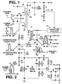
- FIGURE 1 is a schematic diagram of an overvoltage protection system for a television.
- FIGURE 2 is a timing diagram illustrating the relative phase of filament and HVR pulses generated in the circuit of FIGURE 1.
- FIGURE 3 is an isoexposure graph useful for explaining inventive arrangements.
- An overvoltage protection system 10 comprising a circuit for generating an ultor voltage, or high voltage, HV and an X-radiation protection circuit is shown in FIGURE 1.
- a first resonant retrace circuit 20, for implementing horizontal deflection, comprises a source of horizontal drive signals (not shown), a horizontal output transistor Q1, a retrace capacitor C1, a damper diode D1 and a flyback transformer Tr1.
- Transformer Tr1 has a winding W1 connected to transistor Q1, capacitor C1 and diode D1 for generating the B+ voltage.
- a first voltage signal V1 is induced in winding W2, which forms part of the high voltage generating circuit.
- the first voltage signal is approximately 29.5 KV, in accordance with the isoexposure graph shown in FIGURE 3.
- An auxiliary winding W3 generates a filament pulse FP which has an amplitude, or energy level, proportional to the voltage induced in winding W2.
- the filament pulse FP is a first feedback pulse, or signal, which is supplied to summing junction ⁇ 1 through resistor R3.
- a boost voltage circuit 30 comprises a second transformer Tr2, a second transistor Q2 switched by a horizontal drive signal, and a flyback capacitor C3 in parallel with winding W5 of transformer Tr2.
- a second voltage signal V2 is induced in winding W4 of transformer Tr2, which is connected in series with winding W2 and a diode D2, representative of an ultor voltage generating diode set.
- the second voltage signal is approximately 2.5 KV.
- the first and second voltage signals are summed by the series connected windings and develop a high voltage signal HV at capacitor C2.
- Capacitor C2 represents a combination of the kine capacitance and the capacitance of the high voltage splitter.
- a voltage divider formed by resistors R1 and R2 provides a feedback signal to a high voltage regulator 32, which may be embodied as a series pass regulator. The voltage divider provides a reduction factor of approximately 1/300.
- the boost voltage is regulated by having the drain of transistor Q2 switch the resonant circuit formed by winding W5 and capacitor C3 creating the high voltage regulating (HVR) pulse.
- the HVR pulse will range between approximately 50 V peak and 400 V peak, depending upon the operation of the regulator 32.
- the HVR pulse is also supplied to summing junction ⁇ 1 as a second feedback pulse, through resistor R4.
- the filament pulse FP is narrower than the HVR pulse, and will have a lower amplitude under normal conditions.
- the summing junction ⁇ 1 produces a combination feedback pulse having contributions of both inputs to the summing junction. It can be seen that the combination feedback pulse is not symmetric. As shown in FIGURE 2, the filament pulse occurs earlier in time. This results from diode D2 initiating conduction approximately at the trailing edge (right edge in the FIGURE) of the filament pulse.
- an overvoltage protection circuit comprises a voltage sensing circuit 40 and a trip circuit 50.
- the distinction between circuits 40 and 50 is somewhat arbitrary, and made for convenience in description.
- Successive combination feedback pulses are rectified by diode D3 and develop a voltage level across capacitor C5.
- a filter capacitor C4 is in parallel with diode D3.
- Resistors R5, which is adjustable, R6, R7 and R8 determine the bias level at the base of transistor Q3.
- the voltage level is coupled to the emitter of transistor Q3 through Zener diode Z1 and resistor R9, when Zener diode Z1 is biased for reverse conduction. Zener diode Z1 is rated for 10 volts.
- Transistor Q3 will conduct when the emitter to base voltage exceeds approximately 0.7 volts. This will occur when the voltage Vtrip across resistor R7 exceeds approximately 10.7 volts. This can be set rather precisely by adjustment of resistor R5.
- Trip circuit 50 includes a silicon controlled rectifier SCR1, which is normally nonconductive.
- the anode of SCR1 is normally high, in the logic sense. Conduction of transistor Q3 charges capacitor C6. When the voltage across capacitor C6 is high enough, SCR1 will be gated into conduction. The anode of SCR1 will be pulled to ground. The anode of SCR1 therefor provides an ON/OFF signal for X-radiation protection.
- the control signal can be used for disabling the power supply and/or the horizontal deflection circuit and/or the boost circuit and/or as a command signal to a microprocessor, which would in turn disable some or all of the television circuitry to prevent generation of X-radiation.
- Tracking the high voltage and combining the two feedback pulse signals for defining the trip voltage Vtrip each contribute to defining an operating curve which is much closer to the isoexposure curve than would be possible with known circuits, as shown in FIGURE 3, without sacrificing safety.
- the tolerances of only a small number of resistors are important for precise control.
- Resistors R7, R8 and R9 have a 1% tolerance and resistors R3 and R4 have a 2% tolerance. This reduces the cost of the overvoltage protection circuit and contributes to the need for a smaller pad between the operating curve and the isoexposure curve.
Landscapes
- Engineering & Computer Science (AREA)
- Multimedia (AREA)
- Signal Processing (AREA)
- Details Of Television Scanning (AREA)
- Emergency Protection Circuit Devices (AREA)
Description
- This invention relates generally to the field of overvoltage protection systems for television apparatus, and in particular, to an X-radiation protection circuit which enables television apparatus to operate at ultor voltage levels which are closer to the isoexposure curves of cathode ray tubes.
- It is normally desirable to operate a picture tube at the highest ultor voltage possible, due to concerns with beam spot size and circuit configuration and limitations in general. One of the limitations on how high the ultor voltage can be is the ultor voltage level at which X-radiation is generated. The Center for Devices and Radiological Health, part of the Food and Drug Administration, sets limits on the maximum permissible X-radiation and a cathode ray tube vendor will specify what the ultor voltage versus beam current relationship is for each particular tube is which will result in generation of X-radiation. This relationship is expressed as an isoexposure curve. An isoexposure curve is shown in a graph in FIGURE 3. The isoexposure curve represents X-radiation at a level of 0.5 milliRoentgens per hour (mR/Hr). The Y axis is the ultor, or high voltage level designated HV. The X axis is beam current (IBEAM), denoted in milliamps (ma). For the curve shown, a maximum beam current level of approximately 2 ma exceeds the safe level defined by the isoexposure curve at approximately 38 KV. In accordance with the safety rules, a television chassis shall not be allowed to drive a picture tube to any HV vs. IBEAM point which exceeds the isoexposure curve. It is also required that these excessive conditions cannot exist even with only one fault in the chassis. This fault can occur in any circuit, including for example the high voltage circuit, the X-ray protection (XRP) circuit and the power supply; or can result from any component value change.
- Figure 3 also shows two operating curves. The upper curve is designated with tracking high voltage HV and the lower curve is designated without tracking high voltage HV. The lower operating curve represents operation without benefit of the invention taught herein. The upper operating curve represents operation in accordance with the invention taught herein. Normal operation of the chassis would be at HV vs. IBEAM levels below the isoexposure curve. A fourth curve in the graph, between the operating curve(s) and the isoexposure curve is the XRP circuit trip curve, that is, the voltage level at which the XRP circuit disables the television in a manner which prevents generation of X-radiation, for example by shutting down the high voltage power supply.
- There are tolerances associated with each of these curves which tend to widen the distance between the operating curve(s) and the isoexposure curve. These tolerances are an inherent aspect of essentially all electrical circuits and components, such as the XRP circuit, the high voltage regulator and the operating characteristics for a particular picture tube. There must be enough separation between the isoexposure curve and the operating curve to avoid X-radiation under worst case circumstances of normal operation. This separation is often referred to as the pad.
- Ultor voltage is ordinarily generated in a flyback transformer of a resonant retrace horizontal deflection circuit. Such a circuit might generate 29 KV. Some picture tubes require still higher ultor voltages for proper operation. A second resonant retrace circuit having a second flyback transformer can generate a boost voltage, for example 3 KV. The appropriate windings of the flyback transformers of the two resonant retrace circuits are coupled in series to generate an ultor voltage which is the sum of the two voltages, 32 KV in this example. However, with prior art overvoltage protection systems, in which the high voltage from the second circuit was not tracked, it was necessary to add the maximum boost voltage of the high voltage regulator to the amount that the operating curve must be decreased below the isoexposure and XRP trip curves. Such a limitation made it more difficult to operate safely at ultor voltage levels closer to the isoexposure and XRP trip curves, notwithstanding the boost voltage.
- The XRP circuit is a circuit which detects the value of the kine ultor (HV) voltage and will shut down the HV power supply if the HV reaches a certain voltage. This voltage is determined by the kine X-radiation characteristics. In one known method of operation, a peak detected voltage from the HV transformer is used to indicate the value of HV. This peak detected voltage is not generated by the same winding as the HV, but is on the same transformer and therefore proportional to the HV. In another known method, a HV regulator is used which regulates by inserting a pulse voltage in series with the HV transformer winding which generates HV. Therefore, the high voltage is the peak detected sum of the HV winding voltage and the HV regulator winding voltage. The XRP voltage is not proportional to the HV in this configuration, but is proportional only to the portion of the HV that is generated by the HV transformer. If the isoexposure curves are high enough, such as in certain projection televisions, a large pad can be added to compensate for whatever the HV regulator may boost. Most direct view chassis do not have the luxury of sufficient voltage to allow for this pad between the nominal operating HV and the HV where X-radiation is emitted.
- US-A- 5,047,698 discloses a high voltage shutdown circuit having first and second transformer windings that are coupled in series for producing corresponding first and second flyback pulses. A first protection circuit disables the generation of each of the pulse voltages when the amplitude of the first pulse voltage becomes excessive. A second protection circuit disables the generation of each of the pulse voltages when the amplitude of the second pulse voltage becomes excessive.
- US 4,145,639 discloses a television receiver protection circuit having means for generating first and second deflection voltages. An overprotection circuit combines the first and second voltages to produce a fault signal. When the fault signal is present, the overprotection circuit generates a disabling signal.
- The invention is set out in
claim 1. - An overvoltage protection system according to the inventive arrangements taught herein results in a feedback voltage which is directly proportional to HV when a HV boost regulator is being used. The high voltage is therefor closely tracked, which in turn enables the operating curve to be much closer to the isoexposure curve without risking generation of X-radiation or causing frequent interruptions in operation of the television.
- In such an overvoltage protection system, a first resonant retrace circuit is operable for generating a first voltage signal and a second resonant retrace circuit coupled to the first resonant retrace circuit is operable for generating a second voltage signal summed with the first voltage signal. An auxiliary winding of a flyback transformer in the first resonant retrace circuit generates a first feedback signal representative of the first voltage signal. A regulator senses the summed first and second voltage signals and generates a second feedback signal representative of the summed first and second voltage signals. The second resonant retrace means is responsive to the regulator. A resistive summing junction combines the first and second feedback signals to generate a composite feedback signal. An overvoltage protection circuit is responsive to the composite feedback signal for disabling operation of at least one of the first and second resonant retrace circuits.
- FIGURE 1 is a schematic diagram of an overvoltage protection system for a television.
- FIGURE 2 is a timing diagram illustrating the relative phase of filament and HVR pulses generated in the circuit of FIGURE 1.
- FIGURE 3 is an isoexposure graph useful for explaining inventive arrangements.
- An
overvoltage protection system 10 comprising a circuit for generating an ultor voltage, or high voltage, HV and an X-radiation protection circuit is shown in FIGURE 1. A firstresonant retrace circuit 20, for implementing horizontal deflection, comprises a source of horizontal drive signals (not shown), a horizontal output transistor Q1, a retrace capacitor C1, a damper diode D1 and a flyback transformer Tr1. Transformer Tr1 has a winding W1 connected to transistor Q1, capacitor C1 and diode D1 for generating the B+ voltage. A first voltage signal V1 is induced in winding W2, which forms part of the high voltage generating circuit. The first voltage signal is approximately 29.5 KV, in accordance with the isoexposure graph shown in FIGURE 3. An auxiliary winding W3 generates a filament pulse FP which has an amplitude, or energy level, proportional to the voltage induced in winding W2. The filament pulse FP is a first feedback pulse, or signal, which is supplied to summing junction Σ1 through resistor R3. - A
boost voltage circuit 30 comprises a second transformer Tr2, a second transistor Q2 switched by a horizontal drive signal, and a flyback capacitor C3 in parallel with winding W5 of transformer Tr2. A second voltage signal V2 is induced in winding W4 of transformer Tr2, which is connected in series with winding W2 and a diode D2, representative of an ultor voltage generating diode set. The second voltage signal is approximately 2.5 KV. The first and second voltage signals are summed by the series connected windings and develop a high voltage signal HV at capacitor C2. Capacitor C2 represents a combination of the kine capacitance and the capacitance of the high voltage splitter. A voltage divider formed by resistors R1 and R2 provides a feedback signal to ahigh voltage regulator 32, which may be embodied as a series pass regulator. The voltage divider provides a reduction factor of approximately 1/300. - The boost voltage is regulated by having the drain of transistor Q2 switch the resonant circuit formed by winding W5 and capacitor C3 creating the high voltage regulating (HVR) pulse. The HVR pulse will range between approximately 50 V peak and 400 V peak, depending upon the operation of the
regulator 32. The HVR pulse is also supplied to summing junction Σ1 as a second feedback pulse, through resistor R4. As illustrated, the filament pulse FP is narrower than the HVR pulse, and will have a lower amplitude under normal conditions. The summing junction Σ1 produces a combination feedback pulse having contributions of both inputs to the summing junction. It can be seen that the combination feedback pulse is not symmetric. As shown in FIGURE 2, the filament pulse occurs earlier in time. This results from diode D2 initiating conduction approximately at the trailing edge (right edge in the FIGURE) of the filament pulse. - With reference again to FIGURE 1, an overvoltage protection circuit comprises a
voltage sensing circuit 40 and atrip circuit 50. The distinction betweencircuits -
Trip circuit 50 includes a silicon controlled rectifier SCR1, which is normally nonconductive. The anode of SCR1 is normally high, in the logic sense. Conduction of transistor Q3 charges capacitor C6. When the voltage across capacitor C6 is high enough, SCR1 will be gated into conduction. The anode of SCR1 will be pulled to ground. The anode of SCR1 therefor provides an ON/OFF signal for X-radiation protection. The control signal can be used for disabling the power supply and/or the horizontal deflection circuit and/or the boost circuit and/or as a command signal to a microprocessor, which would in turn disable some or all of the television circuitry to prevent generation of X-radiation. - Tracking the high voltage and combining the two feedback pulse signals for defining the trip voltage Vtrip each contribute to defining an operating curve which is much closer to the isoexposure curve than would be possible with known circuits, as shown in FIGURE 3, without sacrificing safety. Moreover, the tolerances of only a small number of resistors are important for precise control. Resistors R7, R8 and R9 have a 1% tolerance and resistors R3 and R4 have a 2% tolerance. This reduces the cost of the overvoltage protection circuit and contributes to the need for a smaller pad between the operating curve and the isoexposure curve.
Claims (7)
- An overvoltage protection system for a television apparatus, comprising: first resonant retrace means (20) operable for generating a first voltage signal (V1);characterized by:second resonant retrace means (30) coupled to said first resonant retrace means (20) and operable for generating a second voltage signal (V2) summed with said first voltage signal (V1);means (W3, R3) for generating a first feedback signal (FP) representative of said first voltage signal (V1); and,an overvoltage protection circuit (40, 50) for disabling operation of at least one of said first and second resonant retrace means (20, 30);means (R4) for generating a second feedback signal (HVR) representative of said summed first and second voltage signals (HV);means (Σ1, D3, C5) for combining said first and second feedback signals to generate a composite feedback signal; and,said overvoltage protection circuit (40, 50) being responsive to said composite feedback signal.
- The system of claim 1, wherein:said first resonant retrace means (20) is characterized by a first flyback transformer (Tr1) having a primary winding (W1) coupled between a first source of supply voltage (B+) and a first switching circuit (Q1), a secondary winding (W2) for generating said first voltage signal (V1) and an auxiliary winding (W3) for generating said first feedback signal (FP); and,said second resonant retrace means (30) is characterized by a second flyback transformer (Tr2), having a primary winding (W5) coupled between a second source of supply voltage, representative of said summed first and second voltages (HV), and a second switching circuit (Q2) and a secondary winding (W4) for generating said second voltage signal (V2) coupled to said secondary winding (W2) of said first flyback transformer (Tr1), said second feedback signal (HVR) being the voltage across said second switching means (Q2).
- The system of claim 1, characterized in that said combining means comprises a resistive summing junction (Σ1).
- The system of claim 1, characterized in that said second resonant retrace means (30) comprises a flyback transformer (Tr2) having a winding (W5) coupled between a source (32) of supply voltage representative of said summed first and second voltages (HV) and a switching circuit (Q2).
- The system according to claim 1 characterized by:first and second transformers (Tr1, Tr2), each having respective windings (W2, W4) coupled in series for generating a high voltage signal (HV) defined by a sum of first and second voltage signals (V1, V2) respectively induced in said respective windings (W2, W4); anda second winding (W3) of said first transformer (Tr1) for generating first feedback pulses (FP), indicative of said first voltage signal (V1).
- The system according to claim 1, characterized in that said means (R3, R4, Σ1) for combining said first and second feedback pulses (FP, HVR) defines successive composite feedback pulses; and
characterized bymeans (D3, C5) for generating a continuous signal indicative of amplitude in said composite feedback pulses; andmeans (40, 50) for sensing said continuous signal and generating a control signal (ON/OFF) for initiating operation of an overvoltage protection circuit when said amplitude of said composite feedback pulses exceeds a predetermined value. - The system of claim 6, wherein said continuous signal is a voltage level signal.
Applications Claiming Priority (2)
| Application Number | Priority Date | Filing Date | Title |
|---|---|---|---|
| US98663592A | 1992-12-01 | 1992-12-01 | |
| US986635 | 1992-12-01 |
Publications (3)
| Publication Number | Publication Date |
|---|---|
| EP0600352A2 EP0600352A2 (en) | 1994-06-08 |
| EP0600352A3 EP0600352A3 (en) | 1995-01-18 |
| EP0600352B1 true EP0600352B1 (en) | 1999-05-12 |
Family
ID=25532610
Family Applications (1)
| Application Number | Title | Priority Date | Filing Date |
|---|---|---|---|
| EP93118867A Expired - Lifetime EP0600352B1 (en) | 1992-12-01 | 1993-11-24 | Overvoltage protection system for televisions |
Country Status (10)
| Country | Link |
|---|---|
| US (1) | US5418705A (en) |
| EP (1) | EP0600352B1 (en) |
| JP (1) | JP3569305B2 (en) |
| KR (1) | KR100311268B1 (en) |
| CN (1) | CN1047050C (en) |
| CA (1) | CA2110002C (en) |
| DE (1) | DE69324892T2 (en) |
| MX (1) | MX9307568A (en) |
| MY (1) | MY111080A (en) |
| SG (1) | SG86969A1 (en) |
Families Citing this family (7)
| Publication number | Priority date | Publication date | Assignee | Title |
|---|---|---|---|---|
| GB9623611D0 (en) * | 1996-11-13 | 1997-01-08 | Rca Thomson Licensing Corp | High voltage regulation by switching retrace capacitors |
| US5982641A (en) * | 1998-08-07 | 1999-11-09 | Thomson Consumer Electronics, Inc. | High-voltage power supply for video display apparatus |
| US6009006A (en) * | 1998-08-07 | 1999-12-28 | Thomson Consumer Electronics, Inc. | Synchronized high voltage generator |
| US6847404B1 (en) | 1998-09-29 | 2005-01-25 | Thomson Licensing S.A. | Video display protection circuit |
| US6252361B1 (en) | 1999-10-15 | 2001-06-26 | Thomson Licensing S.A. | High-voltage power supply disabling circuit for video display |
| DE10243570B3 (en) * | 2002-09-19 | 2004-02-05 | Infineon Technologies Ag | Diode protection circuit, for power supply, has FET in parallel with diode for providing thermal overload protection |
| CN103647261B (en) * | 2013-12-28 | 2016-06-22 | 盖洪儒 | Portable x-ray machine special module protector |
Family Cites Families (14)
| Publication number | Priority date | Publication date | Assignee | Title |
|---|---|---|---|---|
| US3629644A (en) * | 1970-01-15 | 1971-12-21 | Sylvania Electric Prod | High-voltage regulation and protection circuit |
| US3931548A (en) * | 1974-04-26 | 1976-01-06 | Admiral Corporation | Over voltage protection circuit |
| US4126816A (en) * | 1977-05-13 | 1978-11-21 | Rca Corporation | High voltage protection circuit |
| US4145639A (en) * | 1977-10-27 | 1979-03-20 | Rca Corporation | Television receiver protection circuit |
| US4234829A (en) * | 1979-10-01 | 1980-11-18 | Rca Corporation | High voltage disabling circuit for a television receiver |
| US4287535A (en) * | 1979-10-24 | 1981-09-01 | Zenith Radio Corporation | High voltage shutdown circuit with current feedback for cathode ray tube |
| US4335335A (en) * | 1980-02-11 | 1982-06-15 | Rca Corporation | Television receiver high voltage protection circuit |
| US4967121A (en) * | 1987-05-27 | 1990-10-30 | Rca Licensing Corporation | Isolating high voltage transformer for video apparatus |
| GB8805759D0 (en) * | 1988-03-10 | 1988-04-07 | Rca Licensing Corp | Switched-mode power supply with secondary to primary control |
| US4827194A (en) * | 1988-05-06 | 1989-05-02 | Thomson Consumer Electronics, Inc. | Raster size regulating circuit |
| YU47607B (en) * | 1988-06-16 | 1995-10-24 | Siemens Ag. | SWITCHING NETWORK WITH PROTECTION TO LIMIT OUTPUT VOLTAGE |
| US5119262A (en) * | 1988-08-22 | 1992-06-02 | Murata Mfg. Co., Ltd. | High-voltage transformer protection circuit |
| US5047698A (en) * | 1991-03-14 | 1991-09-10 | Thomson Consumer Electronics, Inc. | High voltage shutdown circuit |
| US5111122A (en) * | 1991-05-03 | 1992-05-05 | Thomson Consumer Electronics, Inc. | Video display high voltage protection circuit |
-
1993
- 1993-11-24 EP EP93118867A patent/EP0600352B1/en not_active Expired - Lifetime
- 1993-11-24 SG SG9602449A patent/SG86969A1/en unknown
- 1993-11-24 DE DE69324892T patent/DE69324892T2/en not_active Expired - Fee Related
- 1993-11-25 CA CA002110002A patent/CA2110002C/en not_active Expired - Fee Related
- 1993-11-29 MY MYPI93002518A patent/MY111080A/en unknown
- 1993-11-30 JP JP34106793A patent/JP3569305B2/en not_active Expired - Lifetime
- 1993-11-30 CN CN93112771A patent/CN1047050C/en not_active Expired - Fee Related
- 1993-11-30 KR KR1019930025748A patent/KR100311268B1/en not_active Expired - Fee Related
- 1993-12-01 MX MX9307568A patent/MX9307568A/en not_active IP Right Cessation
-
1994
- 1994-08-30 US US08/309,714 patent/US5418705A/en not_active Expired - Lifetime
Also Published As
| Publication number | Publication date |
|---|---|
| EP0600352A2 (en) | 1994-06-08 |
| SG86969A1 (en) | 2002-03-19 |
| CN1092582A (en) | 1994-09-21 |
| DE69324892T2 (en) | 1999-09-16 |
| KR940017707A (en) | 1994-07-27 |
| JP3569305B2 (en) | 2004-09-22 |
| CA2110002A1 (en) | 1994-06-02 |
| MY111080A (en) | 1999-08-30 |
| MX9307568A (en) | 1994-06-30 |
| CN1047050C (en) | 1999-12-01 |
| US5418705A (en) | 1995-05-23 |
| EP0600352A3 (en) | 1995-01-18 |
| KR100311268B1 (en) | 2001-12-15 |
| CA2110002C (en) | 1999-02-02 |
| DE69324892D1 (en) | 1999-06-17 |
| JPH0746421A (en) | 1995-02-14 |
Similar Documents
| Publication | Publication Date | Title |
|---|---|---|
| US4126816A (en) | High voltage protection circuit | |
| CA1104249A (en) | High voltage protection circuit | |
| US5418705A (en) | Overvoltage protection system for televisions | |
| EP0414184B1 (en) | High voltage regulator circuit for picture tube | |
| EP0642261B1 (en) | Voltage regulator for CRT electrode supply | |
| US4525739A (en) | Television receiver power supply regulation responding to beam current changes | |
| US6282071B1 (en) | Frequency dependent X-ray protection for a multimedia monitor | |
| EP0520141B1 (en) | High voltage shutdown circuit | |
| US4562508A (en) | Regulator fault protection circuit | |
| US5982641A (en) | High-voltage power supply for video display apparatus | |
| GB2239377A (en) | Power regulation during deflection system start up and shut down | |
| JP2781917B2 (en) | Power supply for television receiver | |
| KR0173686B1 (en) | Switched mode power supply and deflection system including hold and reset circuit | |
| EP0370660B1 (en) | Power supply protection circuit | |
| JP3236319B2 (en) | X-ray protection circuit | |
| EP0266995B1 (en) | Video apparatus deflection loss protection | |
| JP3120850B2 (en) | Television equipment power supply | |
| US5111122A (en) | Video display high voltage protection circuit | |
| EP0434075B1 (en) | Vertical yoke protection system | |
| JP3201476B2 (en) | Television deflection device | |
| JP2595030B2 (en) | CRT protection circuit | |
| JPH07254996A (en) | Horizontal deflection circuit | |
| HK1003240B (en) | Video apparatus deflection loss protection |
Legal Events
| Date | Code | Title | Description |
|---|---|---|---|
| PUAI | Public reference made under article 153(3) epc to a published international application that has entered the european phase |
Free format text: ORIGINAL CODE: 0009012 |
|
| AK | Designated contracting states |
Kind code of ref document: A2 Designated state(s): DE GB IT |
|
| PUAL | Search report despatched |
Free format text: ORIGINAL CODE: 0009013 |
|
| AK | Designated contracting states |
Kind code of ref document: A3 Designated state(s): DE GB IT |
|
| 17P | Request for examination filed |
Effective date: 19950617 |
|
| 17Q | First examination report despatched |
Effective date: 19970926 |
|
| GRAG | Despatch of communication of intention to grant |
Free format text: ORIGINAL CODE: EPIDOS AGRA |
|
| GRAG | Despatch of communication of intention to grant |
Free format text: ORIGINAL CODE: EPIDOS AGRA |
|
| GRAH | Despatch of communication of intention to grant a patent |
Free format text: ORIGINAL CODE: EPIDOS IGRA |
|
| GRAH | Despatch of communication of intention to grant a patent |
Free format text: ORIGINAL CODE: EPIDOS IGRA |
|
| GRAA | (expected) grant |
Free format text: ORIGINAL CODE: 0009210 |
|
| AK | Designated contracting states |
Kind code of ref document: B1 Designated state(s): DE GB IT |
|
| REF | Corresponds to: |
Ref document number: 69324892 Country of ref document: DE Date of ref document: 19990617 |
|
| PLBE | No opposition filed within time limit |
Free format text: ORIGINAL CODE: 0009261 |
|
| STAA | Information on the status of an ep patent application or granted ep patent |
Free format text: STATUS: NO OPPOSITION FILED WITHIN TIME LIMIT |
|
| 26N | No opposition filed | ||
| REG | Reference to a national code |
Ref country code: GB Ref legal event code: IF02 |
|
| REG | Reference to a national code |
Ref country code: GB Ref legal event code: 746 Effective date: 20030103 |
|
| PGFP | Annual fee paid to national office [announced via postgrant information from national office to epo] |
Ref country code: DE Payment date: 20081121 Year of fee payment: 16 |
|
| PGFP | Annual fee paid to national office [announced via postgrant information from national office to epo] |
Ref country code: IT Payment date: 20081127 Year of fee payment: 16 |
|
| PGFP | Annual fee paid to national office [announced via postgrant information from national office to epo] |
Ref country code: GB Payment date: 20081028 Year of fee payment: 16 |
|
| GBPC | Gb: european patent ceased through non-payment of renewal fee |
Effective date: 20091124 |
|
| PG25 | Lapsed in a contracting state [announced via postgrant information from national office to epo] |
Ref country code: DE Free format text: LAPSE BECAUSE OF NON-PAYMENT OF DUE FEES Effective date: 20100601 |
|
| PG25 | Lapsed in a contracting state [announced via postgrant information from national office to epo] |
Ref country code: GB Free format text: LAPSE BECAUSE OF NON-PAYMENT OF DUE FEES Effective date: 20091124 |
|
| PG25 | Lapsed in a contracting state [announced via postgrant information from national office to epo] |
Ref country code: IT Free format text: LAPSE BECAUSE OF NON-PAYMENT OF DUE FEES Effective date: 20091124 |