EP0596689A2 - Magnetoresistive Sensor - Google Patents
Magnetoresistive Sensor Download PDFInfo
- Publication number
- EP0596689A2 EP0596689A2 EP93308726A EP93308726A EP0596689A2 EP 0596689 A2 EP0596689 A2 EP 0596689A2 EP 93308726 A EP93308726 A EP 93308726A EP 93308726 A EP93308726 A EP 93308726A EP 0596689 A2 EP0596689 A2 EP 0596689A2
- Authority
- EP
- European Patent Office
- Prior art keywords
- layer
- layers
- ferromagnetic material
- magnetic
- magnetoresistive sensor
- Prior art date
- Legal status (The legal status is an assumption and is not a legal conclusion. Google has not performed a legal analysis and makes no representation as to the accuracy of the status listed.)
- Granted
Links
Images


Classifications
-
- G—PHYSICS
- G11—INFORMATION STORAGE
- G11B—INFORMATION STORAGE BASED ON RELATIVE MOVEMENT BETWEEN RECORD CARRIER AND TRANSDUCER
- G11B5/00—Recording by magnetisation or demagnetisation of a record carrier; Reproducing by magnetic means; Record carriers therefor
- G11B5/127—Structure or manufacture of heads, e.g. inductive
- G11B5/33—Structure or manufacture of flux-sensitive heads, i.e. for reproduction only; Combination of such heads with means for recording or erasing only
- G11B5/39—Structure or manufacture of flux-sensitive heads, i.e. for reproduction only; Combination of such heads with means for recording or erasing only using magneto-resistive devices or effects
- G11B5/3903—Structure or manufacture of flux-sensitive heads, i.e. for reproduction only; Combination of such heads with means for recording or erasing only using magneto-resistive devices or effects using magnetic thin film layers or their effects, the films being part of integrated structures
-
- B—PERFORMING OPERATIONS; TRANSPORTING
- B82—NANOTECHNOLOGY
- B82Y—SPECIFIC USES OR APPLICATIONS OF NANOSTRUCTURES; MEASUREMENT OR ANALYSIS OF NANOSTRUCTURES; MANUFACTURE OR TREATMENT OF NANOSTRUCTURES
- B82Y10/00—Nanotechnology for information processing, storage or transmission, e.g. quantum computing or single electron logic
-
- B—PERFORMING OPERATIONS; TRANSPORTING
- B82—NANOTECHNOLOGY
- B82Y—SPECIFIC USES OR APPLICATIONS OF NANOSTRUCTURES; MEASUREMENT OR ANALYSIS OF NANOSTRUCTURES; MANUFACTURE OR TREATMENT OF NANOSTRUCTURES
- B82Y25/00—Nanomagnetism, e.g. magnetoimpedance, anisotropic magnetoresistance, giant magnetoresistance or tunneling magnetoresistance
-
- G—PHYSICS
- G11—INFORMATION STORAGE
- G11B—INFORMATION STORAGE BASED ON RELATIVE MOVEMENT BETWEEN RECORD CARRIER AND TRANSDUCER
- G11B5/00—Recording by magnetisation or demagnetisation of a record carrier; Reproducing by magnetic means; Record carriers therefor
- G11B5/127—Structure or manufacture of heads, e.g. inductive
- G11B5/33—Structure or manufacture of flux-sensitive heads, i.e. for reproduction only; Combination of such heads with means for recording or erasing only
- G11B5/39—Structure or manufacture of flux-sensitive heads, i.e. for reproduction only; Combination of such heads with means for recording or erasing only using magneto-resistive devices or effects
- G11B2005/3996—Structure or manufacture of flux-sensitive heads, i.e. for reproduction only; Combination of such heads with means for recording or erasing only using magneto-resistive devices or effects large or giant magnetoresistive effects [GMR], e.g. as generated in spin-valve [SV] devices
Definitions
- the present invention relates generally to magnetic sensors for reading information signals recorded in a magnetic medium and, more particularly, to a magnetoresistive read sensor.
- the prior art discloses a magnetic read transducer referred to as a magnetoresistive (MR) sensor or head which has been shown to be capable of reading data from a magnetic surface at great linear densities.
- An MR sensor detects magnetic field signals through the resistance changes of a read element fabricated of a magnetic material as a function of the strength and direction of magnetic flux being sensed by the read element.
- These prior art MR sensors operate on the basis of the anisotropic magnetoresistive (AMR) effect in which a component of the read element resistance varies as the square of the cosine (cos2) of the angle between the magnetization and the direction of sense current flow through the element.
- AMR anisotropic magnetoresistive
- U.S. Patent No. 4,949,039 to Grunberg describes a layered magnetic structure which yields enhanced MR effects caused by antiparallel alignment of the magnetizations in the magnetic layers.
- Grunberg lists ferromagnetic transition metals and alloys, but does not indicate preferred materials from the list for superior MR signal amplitude.
- Grunberg further describes the use of antiferromagnetic-type exchange coupling to obtain the antiparallel alignment in which adjacent layers of ferromagnetic materials are separated by a thin interlayer of chromium (Cr) or yttrium (Y).
- European Patent Application EP-A-490608 discloses an MR sensor in which the resistance between two uncoupled ferromagnetic layers is observed to vary as the cosine of the angle between the magnetizations of the two layers and which is independent of the direction of current flow through the sensor. This mechanism produces a magnetoresistance that, for selected combinations of materials, is greater in magnitude than the AMR, and is referred to as giant magnetoresistance or the "spin valve" (SV) magnetoresistance.
- SV spin valve
- Co-pending European Patent Application serial no 93306379.4 describes an MR sensor based on the above-described effect which includes two thin film layers of ferromagnetic material separated by a thin film layer of a non-magnetic metallic material and in which the magnetization of one ferromagnetic layer is maintained perpendicular to the magnetization of the other ferromagnetic layer at zero externally applied magnetic field by exchange coupling with an adjacent layer of antiferromagnetic material.
- a magnetoresistive sensor comprising a layered structure formed on a substrate, the structure comprising, a first, a second and a third layer of ferromagnetic material, each of said layers of ferromagnetic material separated from the adjacent layer of ferromagnetic material by a layer of non-magnetic metallic material, said second layer of ferromagnetic material disposed between said first and third layers of ferromagnetic material, the direction of magnetization being fixed in said first and third layers of ferromagnetic material, the direction of magnetization in said second layer of ferromagnetic material being substantially perpendicular to said fixed directions of magnetization in said first and third layers of ferromagnetic material at zero applied magnetic field.
- a magnetoresistive (MR) read sensor having a multilayered, dual spin valve structure which achieves a large MR response at low applied magnetic fields.
- the MR structure comprises a layered structure formed on a suitable substrate including first, second and third thin film layers of ferromagnetic material separated by thin film layers of non-magnetic metallic material.
- the first and third layers of ferromagnetic material ie, the outer layers of the structure, have their magnetization orientation fixed while the second, intermediate layer of ferromagnetic material is magnetically soft and has its magnetization oriented substantially perpendicular to that of both the outer layers of ferromagnetic material.
- the magnetization directions of the first and third layers of ferromagnetic material can be fixed or "pinned" by any of several methods including hard biasing or exchange biasing by an adjacent antiferromagnetic layer as is known in the art.
- the two outer ferromagnetic layers have their magnetization directions pinned antiparallel to each other and, thus, each pinned layer acts as a magnetic flux keeper for the other pinned layer.
- the magnetization direction of the second, intermediate ferromagnetic layer is free to rotate with an applied magnetic field.
- the electrical resistance of each pair of ferromagnetic layers, i.e., the first and second layers and the second and third layers, varies as a function of the cosine of the angle between the magnetization directions of the two ferromagnetic layers of the pair.
- an MR sensor can be fabricated in which the resistance of the sensor varies from a minimum to a maximum value when the magnetization direction of the intermediate, free layer rotates from a direction near parallel to the magnetization of the first, outer pinned layer, for example, to a direction near parallel to the magnetization direction of the third, outer pinned layer.
- a current source provides a sense current to the MR sensor which generates a voltage drop across the read element proportional to the variations in the resistance of the MR sensor due to the rotation of the magnetization in the intermediate, free layer of ferromagnetic material as a function of the applied external magnetic field being sensed.
- a multilayered, dual spin valve sensor in which the magnetization directions in the two outer ferromagnetic layers are parallel with both being perpendicular to the direction of magnetization in the centre, free ferromagnetic layer.
- a magnetic storage system comprising a magnetic storage medium having a plurality of tracks for recording of data; a magnetic transducer maintained in a closely spaced position relative to said magnetic storage medium during relative motion between said magnetic transducer and said magnetic storage medium, said magnetic transducer including a magnetoresistive read sensor according to the first aspect of the present invention; actuator means coupled to said magnetic transducer for moving said magnetic transducer to selected tracks on said magnetic storage medium; and detection means coupled to said magnetoresistive read sensor for detecting resistance changes in said magnetoresistive material responsive to magnetic fields representative of data bits recorded in said magnetic storage medium intercepted by said magnetoresistive sensor.
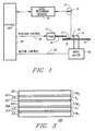
- FIG. 1 Although the invention is described as embodied in a magnetic disk storage system as shown in Fig. 1, it will be apparent that the invention is also applicable to other magnetic recording systems such as a magnetic tape recording system, for example.
- At least one rotatable magnetic disk 12 is supported on a spindle 14 and rotated by a disk drive motor 18.
- the magnetic recording media on each disk is in the form of an annular pattern of concentric data tracks (not shown) on disk 12.
- At least one slider 13 is positioned on the disk 12, each slider 13 supporting one or more magnetic read/write transducers 21, typically referred to as read/write heads. As the disks rotate, the sliders 13 are moved radially in and out over the disk surface 22 so that the heads 21 may access different portions of the disk where desired data is recorded.
- Each slider 13 is attached to an actuator arm 19 by means of a suspension 15.
- the suspension 15 provides a slight spring force which biases the slider 13 against the disk surface 22.
- Each actuator arm 19 is attached to an actuator means 27.
- the actuator means as shown in Fig.1 may be a voice coil motor (VCM), for example.
- the VCM comprises a coil moveable within a fixed magnetic field, the direction and velocity of the coil movements being controlled by the motor current signals supplied by a controller.
- the rotation of the disk 12 generates an air bearing between the slider 13 and the disk surface 22 which exerts an upward force or lift on the slider.
- the air bearing thus counterbalances the slight spring force of the suspension 15 and supports the slider 13 off and slightly above the disk surface by a small, substantially constant spacing during operation.
- control unit 29 The various components of the disk storage system are controlled in operation by control signals generated by control unit 29, such as access control signals and internal clock signals.
- control unit 29 comprises logic control circuits, storage means and a microprocessor, for example.
- the control unit 29 generates control signals to control various system operations such as drive motor control signals on line 23 and head position and seek control signals on line 28.
- the control signals on line 28 provide the desired current profiles to optimally move and position a selected slider 13 to the desired data track on the associated disk 12.
- Read and write signals are communicated to and from read/write heads 21 by means of recording channel 25.
- disk storage systems may contain a large number of disks and actuators, and each actuator may support a number of sliders.
- a preferred embodiment of an MR sensor 30 comprises a first thin film layer 31 of ferromagnetic material, a first thin film layer 33 of a non-magnetic metallic material, a second thin film layer of ferromagnetic material 35, a second thin film layer 37 of a non-magnetic metallic material and a third thin film layer 39 of ferromagnetic material.
- the magnetizations of the two outer layers 31 and 39 of ferromagnetic material are oriented parallel to each other, i.e., in the same direction, and at an angle of about 90 degrees with respect to the magnetization of the intermediate layer 35 of ferromagnetic material in the absence of an externally applied magnetic field as indicated by arrows 32, 34 and 38, respectively.
- the magnetization directions of the first and third outer layers, 31 and 39 of ferromagnetic material are fixed or pinned in a preferred orientation as shown by the arrows 32 and 38.
- the magnetization in the intermediate layer 35 of ferromagnetic material is free to rotate its direction in response to an externally applied magnetic field (such as magnetic field h as shown in Fig. 2), as shown by the dashed arrows 34 on layer 35 in Fig. 2.
- an externally applied magnetic field such as magnetic field h as shown in Fig. 2
- the ferromagnetic layers 31, 35 and 39 can be fabricated of any suitable magnetic material such as cobalt (Co), iron (Fe), nickel (Ni) and their alloys such as nickel-iron (NiFe), nickel-cobalt (NiCo) and iron-cobalt (FeCo), for example.
- the non-magnetic metallic spacer layers 33 and 37 comprise copper (Cu), for example, or other suitable noble metal such as silver (Ag) or gold (Au) or their alloys.
- the fixed or pinned outer ferromagnetic layers 31 and 39 can be exchange biased by adjacent layers (as shown in Fig. 9) of an antiferromagnetic material such as iron-manganese (FeMn), for example.
- an MR sensor based on the spin valve effect wherein a pinned ferromagnetic layer is exchanged biased by an adjacent antiferromagnetic layer is described in greater detail in the above referenced European patent application 93306379.4.
- the magnetization directions of the pinned ferromagnetic layers 31, 39 can be fixed by use of an adjacent hard magnetic layer or by use of a material having a sufficiently high coercivity for the outer pinned layers 31, 39.
- the structure of a conventional or single spin valve MR sensor as described in the above-cited patent applications is essentially FM free /NM/FM pinned /AFM where FM free and FM pinned are ferromagnetic layers separated by a non-magnetic layer NM.
- the orientation of the magnetization of the FM pinned layer is fixed up to some moderate magnetic field by the exchange coupled bias field provided by the antiferromagnetic layer AFM.
- the magnetoresistive effect of the sensor is based on the fact that, when the directions of the magnetization in the adjacent FM layers are different, conduction electrons traversing the NM layer from one FM layer to the other are scattered depending on their spins such that the resistance of the sensor increases.
- This change in resistance is a function of the cosine of the angle between the directions of the magnetizations in the FM layers and is minimum when the magnetizations are parallel, i.e., in the same direction, and maximum when the magnetizations in the layers antiparallel, i.e., in opposite directions.
- the structure described above with reference to Fig. 2 comprises a "dual" spin valve wherein the spin valve structure is doubled symmetrically with respect to the FM free layer.
- the structure of a dual spin valve is AFM1/FM p1 /NM1/FM free /NM2/FM p2 /AFM2 providing two pairs of FM layers separated by a NM layer which allows utilization of the conduction electrons scattered in both directions from the intermediate FM free layer.
- the directions of magnetization in the two pinned outer layers, FM p1 and FM p2 are fixed by adjacent antiferromagnetic layers AFM1 and AFM2, respectively, while the direction of magnetization in the FM free layer is allowed to rotate freely in response to an applied free magnetic field.
- a dual spin valve sensor comprises the structure FM1/S1/FM2/S2/FM3 as shown.
- the first ferromagnetic layer FM1 comprises a layer of a first ferromagnetic material 311, such as NiFe, for example, and a thin layer 313, referred to as a "nanolayer", of a second ferromagnetic material, such as Co, for example.
- the nanolayer 313 of the second ferromagnetic material is deposited at the interface between the first ferromagnetic layer and the first spacer layer 371.
- the first ferromagnetic layer forms a bilayer 311, 313 of two different ferromagnetic materials.
- the third ferromagnetic layer FM3 comprises a bilayer 301, 303 of two different ferromagnetic materials with the nanolayer 303 formed at the interface between the third ferromagnetic layer FM3 and the second spacer layer 331.
- the second ferromagnetic layer FM2 Since the second, central ferromagnetic layer FM2 forms an interface with both spacer layers 331 and 371, the second ferromagnetic layer FM2 will comprise a trilayer having a centre layer 305 of ferromagnetic material, such as NiFe, for example, with a nanolayer 309, 307 of a second ferromagnetic material, such as Co, for example, formed at the interface with each of the adjacent spacer layers 371, 331, respectively.
- the thickness of the nanolayers is in the range of 0.05 to 2 nm (0.5 to 20 Angstroms).
- the nanolayer can be formed within the ferromagnetic layer at a distance X from the interface between the ferromagnetic layer and the spacer layer.
- the material utilized for the nanolayer can be a non-magnetic material, such as Cr, for example, as well as a ferromagnetic material.
- Magnetoresistive sensors employing nanolayers as described above are described in greater detail in EP-A-529959 (published 3/3/93)
- the thickness of the layers is optimized to provide the highest value of magnetoresistance obtainable for these materials in this structure.
- a preferred embodiment of the dual spin valve formed on a Si substrate having the structure Si/50Ta/20NiFe/110FeMn/60NiFe/25Cu/100NiFe/25Cu/60NiFe/ 110FeMn/50Ta provides a magnetoresistance of 5.5 percent, a 35 percent increase over that obtained from the single spin valve structure.
- the first NiFe layer in the above dual spin valve structure provides a seed layer utilized to obtain the necessary crystalline structure to provide antiferromagnetic FeMn; any material having sufficiently high resistivity to minimize current shunting and which permits the growth of an antiferromagnetic form of FeMn is suitable for use as the seed layer.
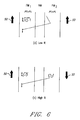
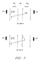
- a dual spin valve MR sensor can be designed wherein the directions of the magnetizations in the outer, pinned ferromagnetic layers are maintained antiparallel to each other, ie, in opposite directions. Further, by proper choice of materials for the different layers, both positive and negative spin-dependent magnetoresistance, referred to as giant magnetoresistance (GMR), can be utilized to produce a high value of (delta R)/R for the sensor. As shown in Fig.
- GMR giant magnetoresistance
- a single spin valve structure having positive GMR comprises two ferromagnetic layers, FM1 and FM2, separated by a nonmagnetic layer, NM, wherein for both ferromagnetic layers the resistivities for spin-up (rho up ) and spin-down (rho down ) satisfy either the relation rho up >rho down or the relation rho up ⁇ rho down .
- the resistance is minimum when the magnetizations, as indicated by arrows 50, of the layers FM1 and FM2 are parallel and maximum when the magnetizations of the layers FM1 and FM2 are antiparallel. As shown in Fig.
- a single spin valve structure having negative GMR comprises two ferromagnetic layers separated by a nonmagnetic layer wherein for the first ferromagnetic layer, FM1, rho up >rho down and for the second ferromagnetic layer, FM2, rho up ⁇ rho down .
- the resistance is minimum for antiparallel alignment of the magnetizations, as indicated by arrows 60, and maximum for parallel alignment of the magnetizations.
- Fig. 8 illustrates three ferromagnetic layers according to the present invention.
- the GMR is positive producing minimum resistance for parallel alignment of their magnetizations, arrows 71 and 73, respectively.
- the GMR is positive so that minimum resistance is produced for antiparallel alignment of their magnetizations, arrows 73 and 75, respectively.
- the net effect for the structure is that the resistance is maximum when the magnetization of the free layer FM2, arrow 73, is aligned parallel with the magnetization of pinned layer FM3 , arrow 75, and minimum when the magnetization of FM2 is aligned parallel with the magnetization of pinned layer FM1, arrow 71. Additionally, since the magnetizations of the two pinned layers, FM1 and FM2, are aligned in opposite directions, each layer acts as a magnetic flux-keeper for the other layer, thus reducing the demagnetizing effect of the pinned layers.
- an MR sensor 40 comprises a first thin film layer 51 of antiferromagnetic material, a first thin film layer 41 of ferromagnetic material, a first thin film layer 43 of a non-magnetic metallic material, a second thin film layer 45 of ferromagnetic material, a second thin film layer 47 of a non-magnetic metallic material, a third thin film layer 49 of ferromagnetic material and a second thin film layer 53 of antiferromagnetic material.
- the two antiferromagnetic layers 51 and 53 provide a bias field in the adjacent ferromagnetic layers 41 and 49, respectively, by exchange coupling, as is known in the art.
- the magnetizations, as indicated by arrows 42 and 48, respectively, of the two outer ferromagnetic layers 41 and 49 are oriented antiparallel to each other, i.e., in opposite directions, and at an angle of about 90 degrees with respect to the magnetization, as indicated by arrow 44, of the intermediate layer 45 of ferromagnetic material in the absence of an externally applied magnetic field.
- the magnetization direction of the first and third outer layers, 41 and 49 of ferromagnetic material are fixed or pinned in the preferred orientation as shown by the arrows 42 and 48 by the exchange bias of the antiferromagnetic layers 51 and 53, respectively.
- exchange bias layers 51 and 53 comprise different antiferromagnetic materials, preferably FeMn and nickel-manganese (NiMn), respectively, for example.
- the two antiferromagnetic materials have different blocking temperatures, thus allowing the exchange bias direction of each antiferromagnetic layer 51, 53 to be set independent of the other.
- the blocking temperature for the FeMn is approximately 220 degrees C while the blocking temperature for NiMn is much higher.
- the exchange bias direction for the NiMn layer is first set at a relatively high temperature, about 260 degrees C, for example, then the exchange bias direction for the FeMn layer is set a lower temperature, just slightly above the blocking temperature for FeMn, about 230 degrees C, for example.
- a seed layer can be used to insure that the antiferromagnetic layers 51, 53 have the desired structure.
- the materials for the ferromagnetic layers 41, 45 and 49 are chosen to utilize both positive and negative GMR layer pairs. As described above with reference to Fig. 7, materials are chosen such that between the first and second ferromagnetic layers 41 and 45 the GMR is positive, and that between the second and third ferromagnetic layers 45 and 49 the GMR is negative.
- Dilute alloys of vanadium (V) or chromium (Cr) in a Ni or Fe matrix provide ferromagnetic materials wherein rho up >rho down
- Fe or Co in a Ni matrix provide ferromagnetic materials wherein rho up ⁇ rho down , for example.
- Spin-dependent resistivities for Fe or Co diluted with aluminum (Al), iridium (Ir) or Mn are also known.
- the non-magnetic spacer layers 43 and 47 can be any suitable non-magnetic metallic material such as Cu, Au or Ag, for example.
- a suitable underlayer 57 such as Ta, Ru or CrV, for example, is deposited on substrate 55 prior to the deposition of a first antiferromagnetic exchange bias layer 59.
- the purpose of underlayer 57 is to optimize the texture, grain size and morphology of the subsequent layers.
- the morphology can be crucial in obtaining the large MR effects characteristic of dual spin valve structures since it permits the use of very thin non-magnetic metallic spacer layers 63 and 65 between the ferromagnetic layers 61, 65 and 69.
- the underlayer must also have a high resistivity to minimize electrical current shunting effects.
- the underlayer 57 can be omitted.
- Any suitable antiferromagnetic magnetic material may be utilized for the exchange bias layer 59 such as FeMn or NiMn, for example.
- FeMn(60/40 by atomic weight) results in a reduction of the coupling field between the following two ferromagnetic layers where the FeMn antiferromagnetic layer is deposited first.
- a seed layer (not shown) may also be required if the material utilized for the first antiferromagnetic layer 59 cannot be directly deposited with the proper crystalline structure.
- a seed layer preferably of NiFe or AuCu, is desirable to ensure that the antiferromagnetic form of FeMn is obtained.
- a first thin film layer 61 of ferromagnetic material, a first thin film layer 63 of a non-magnetic metallic material, a second thin film layer 65 of ferromagnetic material, a second thin film layer 67 of a non-magnetic metallic material, a third thin film layer 69 of ferromagnetic material and a second thin film exchange bias layer 71 of antiferromagnetic material are deposited over underlayer 57.
- the first and third ferromagnetic layers 61 and 69 have their magnetizations oriented parallel to each other and at an angle of approximately 90 degrees with respect to the magnetization of the second, intermediate ferromagnetic layer 65 in the absence of an applied magnetic field.
- the magnetization directions of the first and third ferromagnetic layers 61 and 69 are fixed or pinned in position by a biasing field produced by exchange coupling.
- the outer ferromagnetic layers 61, 69 can be pinned utilizing an adjacent hard magnetic layer or by utilizing materials having relatively high coercivities for the outer ferromagnetic layers and setting the magnetization directions during fabrication. If the magnetization directions of the outer ferromagnetic layers 61, 69 are different, antiparallel, for example, the coercivity for each layer will have to be different to allow the magnetization direction of one layer to be set independent of the other layer.
- the ferromagnetic layers 61, 65 and 69 can be fabricated of any suitable magnetic material such as Co, Fe, Ni and their alloys such as NiFe, NiCo and FeCo, for example.
- the thicknesses of the ferromagnetic layers 61, 65 and 69 can be selected from a range of about 0.5 nm (5 Angstroms) to about 15 nm (150 Angstroms).
- the non-magnetic spacer layers 63 and 67 are preferably metallic with high conductivity. Noble materials such as Au, Ag and Cu provide large MR response, Pt and Pd provide small MR response, while Cr and Ta exhibit very little MR response.
- the thickness of the non-magnetic spacer layers 63 and 67 is less than the mean free path of the conduction electrons in the sensor, preferably within the range of about 1 nm (10 Angstroms) to about 4 nm (40 Angstroms).
- a longitudinal bias field parallel to the longitudinal direction of the magnetic layers in the sensor in order to minimize Barkhausen noise it is desirable to provide a longitudinal bias field parallel to the longitudinal direction of the magnetic layers in the sensor.
- layers 75 of a suitable magnetically hard material are deposited over the end regions of the sensor thus providing a longitudinal bias field in a central active region 78 of the sensor.
- the longitudinal bias field can be provided by exchange coupling with antiferromagnetic layers formed over the sensor end regions in direct contact with the ferromagnetic layers.
Abstract
Description
- The present invention relates generally to magnetic sensors for reading information signals recorded in a magnetic medium and, more particularly, to a magnetoresistive read sensor.
- The prior art discloses a magnetic read transducer referred to as a magnetoresistive (MR) sensor or head which has been shown to be capable of reading data from a magnetic surface at great linear densities. An MR sensor detects magnetic field signals through the resistance changes of a read element fabricated of a magnetic material as a function of the strength and direction of magnetic flux being sensed by the read element. These prior art MR sensors operate on the basis of the anisotropic magnetoresistive (AMR) effect in which a component of the read element resistance varies as the square of the cosine (cos²) of the angle between the magnetization and the direction of sense current flow through the element. A more detailed description of the AMR effect can be found in "Memory, Storage, and Related Applications", D.A. Thompson et al., IEEE Trans. Mag. MAG-11, p. 1039 (1975).
- More recently, a different, more pronounced magnetoresistive effect has been described in which the change in resistance of a layered magnetic sensor is attributed to the spin-dependent transmission of the conduction electrons between the magnetic layers through a non-magnetic layer and the accompanying spin-dependent scattering at the layer interfaces. This magnetoresistive effect is variously referred to as the "giant magnetoresistive" or "spin valve" effect. Such a magnetoresistive sensor fabricated of the appropriate materials provides improved sensitivity and greater change in resistance than observed in sensors utilizing the AMR effect. In this type of MR sensor, the in-plane resistance between a pair of ferromagnetic layers separated by a non-magnetic layer varies as the cosine (cos) of the angle between the magnetization in the two layers.
- U.S. Patent No. 4,949,039 to Grunberg describes a layered magnetic structure which yields enhanced MR effects caused by antiparallel alignment of the magnetizations in the magnetic layers. As possible materials for use in the layered structure, Grunberg lists ferromagnetic transition metals and alloys, but does not indicate preferred materials from the list for superior MR signal amplitude. Grunberg further describes the use of antiferromagnetic-type exchange coupling to obtain the antiparallel alignment in which adjacent layers of ferromagnetic materials are separated by a thin interlayer of chromium (Cr) or yttrium (Y).
- European Patent Application EP-A-490608 discloses an MR sensor in which the resistance between two uncoupled ferromagnetic layers is observed to vary as the cosine of the angle between the magnetizations of the two layers and which is independent of the direction of current flow through the sensor. This mechanism produces a magnetoresistance that, for selected combinations of materials, is greater in magnitude than the AMR, and is referred to as giant magnetoresistance or the "spin valve" (SV) magnetoresistance.
- Co-pending European Patent Application serial no 93306379.4 describes an MR sensor based on the above-described effect which includes two thin film layers of ferromagnetic material separated by a thin film layer of a non-magnetic metallic material and in which the magnetization of one ferromagnetic layer is maintained perpendicular to the magnetization of the other ferromagnetic layer at zero externally applied magnetic field by exchange coupling with an adjacent layer of antiferromagnetic material.
- According to a first aspect of the present invention there is provided a magnetoresistive sensor comprising a layered structure formed on a substrate, the structure comprising, a first, a second and a third layer of ferromagnetic material, each of said layers of ferromagnetic material separated from the adjacent layer of ferromagnetic material by a layer of non-magnetic metallic material, said second layer of ferromagnetic material disposed between said first and third layers of ferromagnetic material, the direction of magnetization being fixed in said first and third layers of ferromagnetic material, the direction of magnetization in said second layer of ferromagnetic material being substantially perpendicular to said fixed directions of magnetization in said first and third layers of ferromagnetic material at zero applied magnetic field.
- Thus is provided a magnetoresistive (MR) read sensor having a multilayered, dual spin valve structure which achieves a large MR response at low applied magnetic fields. The MR structure comprises a layered structure formed on a suitable substrate including first, second and third thin film layers of ferromagnetic material separated by thin film layers of non-magnetic metallic material. The first and third layers of ferromagnetic material, ie, the outer layers of the structure, have their magnetization orientation fixed while the second, intermediate layer of ferromagnetic material is magnetically soft and has its magnetization oriented substantially perpendicular to that of both the outer layers of ferromagnetic material. In preferred sensors according to this invention, the magnetization directions of the first and third layers of ferromagnetic material can be fixed or "pinned" by any of several methods including hard biasing or exchange biasing by an adjacent antiferromagnetic layer as is known in the art.
- In one preferred embodiment, the two outer ferromagnetic layers have their magnetization directions pinned antiparallel to each other and, thus, each pinned layer acts as a magnetic flux keeper for the other pinned layer. The magnetization direction of the second, intermediate ferromagnetic layer is free to rotate with an applied magnetic field. The electrical resistance of each pair of ferromagnetic layers, i.e., the first and second layers and the second and third layers, varies as a function of the cosine of the angle between the magnetization directions of the two ferromagnetic layers of the pair. For a proper choice of materials, including consideration of the material resistivity as a function of the conduction electron spin, the effect is additive between the two pairs of layers and an MR sensor can be fabricated in which the resistance of the sensor varies from a minimum to a maximum value when the magnetization direction of the intermediate, free layer rotates from a direction near parallel to the magnetization of the first, outer pinned layer, for example, to a direction near parallel to the magnetization direction of the third, outer pinned layer. A current source provides a sense current to the MR sensor which generates a voltage drop across the read element proportional to the variations in the resistance of the MR sensor due to the rotation of the magnetization in the intermediate, free layer of ferromagnetic material as a function of the applied external magnetic field being sensed.
- In a second preferred embodiment of the present invention, a multilayered, dual spin valve sensor is provided in which the magnetization directions in the two outer ferromagnetic layers are parallel with both being perpendicular to the direction of magnetization in the centre, free ferromagnetic layer.
- In a second aspect of the invention there is provided a magnetic storage system comprising a magnetic storage medium having a plurality of tracks for recording of data; a magnetic transducer maintained in a closely spaced position relative to said magnetic storage medium during relative motion between said magnetic transducer and said magnetic storage medium, said magnetic transducer including a magnetoresistive read sensor according to the first aspect of the present invention; actuator means coupled to said magnetic transducer for moving said magnetic transducer to selected tracks on said magnetic storage medium; and detection means coupled to said magnetoresistive read sensor for detecting resistance changes in said magnetoresistive material responsive to magnetic fields representative of data bits recorded in said magnetic storage medium intercepted by said magnetoresistive sensor.
- Preferred embodiments of the invention will now be described, by way of example only, with reference to the accompanying drawings in which:
- Figure 1 is a simplified block diagram of a magnetic disk storage system embodying the present invention;
- Figure 2 is an exploded view in perspective of a preferred embodiment of the magnetoresistive sensor according to the principles of the present invention;
- Figure 3 is an end view of another preferred embodiment of the magnetoresistive sensor according to the principles of the present invention;
- Figure 4 is a graph illustrating the hysteresis loop and the magnetoresistive response for a prior art spin valve MR sensor structure;
- Figure 5 is a graph illustrating the magnetoresistive response for the MR sensor shown in Figure 2;
- Figure 6 is a schematic diagram illustrating a spin valve structure having positive giant magnetoresistance;
- Figure 7 is a schematic diagram illustrating a spin valve structure having negative giant magnetoresistance;
- Figure 8 is a schematic diagram of a dual spin valve utilizing positive and negative giant magnetoresistance according to the principles of the present invention;
- Figure 9 is an exploded view in perspective of another preferred embodiment of the magnetoresistive sensor according to the principles of the present invention; and
- Figure 10 is an end view of another embodiment of a magnetoresistive sensor constructed in accordance with the present invention.
- Referring now to Fig. 1, although the invention is described as embodied in a magnetic disk storage system as shown in Fig. 1, it will be apparent that the invention is also applicable to other magnetic recording systems such as a magnetic tape recording system, for example. At least one rotatable
magnetic disk 12 is supported on aspindle 14 and rotated by adisk drive motor 18. The magnetic recording media on each disk is in the form of an annular pattern of concentric data tracks (not shown) ondisk 12. - At least one
slider 13 is positioned on thedisk 12, eachslider 13 supporting one or more magnetic read/writetransducers 21, typically referred to as read/write heads. As the disks rotate, thesliders 13 are moved radially in and out over thedisk surface 22 so that theheads 21 may access different portions of the disk where desired data is recorded. Eachslider 13 is attached to anactuator arm 19 by means of asuspension 15. Thesuspension 15 provides a slight spring force which biases theslider 13 against thedisk surface 22. Eachactuator arm 19 is attached to an actuator means 27. The actuator means as shown in Fig.1 may be a voice coil motor (VCM), for example. The VCM comprises a coil moveable within a fixed magnetic field, the direction and velocity of the coil movements being controlled by the motor current signals supplied by a controller. - During operation of the disk storage system, the rotation of the
disk 12 generates an air bearing between theslider 13 and thedisk surface 22 which exerts an upward force or lift on the slider. The air bearing thus counterbalances the slight spring force of thesuspension 15 and supports theslider 13 off and slightly above the disk surface by a small, substantially constant spacing during operation. - The various components of the disk storage system are controlled in operation by control signals generated by
control unit 29, such as access control signals and internal clock signals. Typically, thecontrol unit 29 comprises logic control circuits, storage means and a microprocessor, for example. Thecontrol unit 29 generates control signals to control various system operations such as drive motor control signals online 23 and head position and seek control signals online 28. The control signals online 28 provide the desired current profiles to optimally move and position a selectedslider 13 to the desired data track on the associateddisk 12. Read and write signals are communicated to and from read/writeheads 21 by means of recordingchannel 25. - The above description of a typical magnetic disk storage system, and the accompanying illustration of Fig. 1 are for representation purposes only. It should be apparent that disk storage systems may contain a large number of disks and actuators, and each actuator may support a number of sliders.
- Referring now to Fig. 2, a preferred embodiment of an
MR sensor 30 according to the principles of the present invention comprises a firstthin film layer 31 of ferromagnetic material, a firstthin film layer 33 of a non-magnetic metallic material, a second thin film layer offerromagnetic material 35, a secondthin film layer 37 of a non-magnetic metallic material and a thirdthin film layer 39 of ferromagnetic material. The magnetizations of the twoouter layers intermediate layer 35 of ferromagnetic material in the absence of an externally applied magnetic field as indicated byarrows arrows ferromagnetic layers intermediate layer 35 of ferromagnetic material is free to rotate its direction in response to an externally applied magnetic field (such as magnetic field h as shown in Fig. 2), as shown by thedashed arrows 34 onlayer 35 in Fig. 2. - According to this preferred embodiment of the present invention, the
ferromagnetic layers metallic spacer layers ferromagnetic layers ferromagnetic layers layers - The structure of a conventional or single spin valve MR sensor as described in the above-cited patent applications is essentially FMfree/NM/FMpinned/AFM where FMfree and FMpinned are ferromagnetic layers separated by a non-magnetic layer NM. The orientation of the magnetization of the FMpinned layer is fixed up to some moderate magnetic field by the exchange coupled bias field provided by the antiferromagnetic layer AFM. The magnetoresistive effect of the sensor is based on the fact that, when the directions of the magnetization in the adjacent FM layers are different, conduction electrons traversing the NM layer from one FM layer to the other are scattered depending on their spins such that the resistance of the sensor increases. This change in resistance is a function of the cosine of the angle between the directions of the magnetizations in the FM layers and is minimum when the magnetizations are parallel, i.e., in the same direction, and maximum when the magnetizations in the layers antiparallel, i.e., in opposite directions.
- However, it is observed that in the single spin valve structure described above conduction electrons are scattered out of the free FM layer not only towards the pinned FM layer, but in the opposite direction, away from the pinned FM layer as well. Thus, only that portion of the conduction electrons scattered between the two FM layers contribute to the magnetoresistive effect for the sensor.
- The structure described above with reference to Fig. 2 comprises a "dual" spin valve wherein the spin valve structure is doubled symmetrically with respect to the FMfree layer. The structure of a dual spin valve is AFM₁/FMp1/NM₁/FMfree/NM₂/FMp2/AFM₂ providing two pairs of FM layers separated by a NM layer which allows utilization of the conduction electrons scattered in both directions from the intermediate FMfree layer. The directions of magnetization in the two pinned outer layers, FMp1 and FMp2 are fixed by adjacent antiferromagnetic layers AFM₁ and AFM₂, respectively, while the direction of magnetization in the FMfree layer is allowed to rotate freely in response to an applied free magnetic field.
- Referring now also to Fig. 3, an end view of a dual spin valve sensor as described with reference to Figs. 2, 9 and 10 is shown wherein each of the ferromagnetic layers FM₁, FM₂ and FM₃ comprise multiple layers of ferromagnetic materials. As described above, a dual spin valve sensor comprises the structure FM₁/S₁/FM₂/S₂/FM₃ as shown. In this embodiment, the first ferromagnetic layer FM₁ comprises a layer of a first
ferromagnetic material 311, such as NiFe, for example, and athin layer 313, referred to as a "nanolayer", of a second ferromagnetic material, such as Co, for example. Thenanolayer 313 of the second ferromagnetic material is deposited at the interface between the first ferromagnetic layer and thefirst spacer layer 371. Thus, the first ferromagnetic layer forms abilayer bilayer nanolayer 303 formed at the interface between the third ferromagnetic layer FM₃ and thesecond spacer layer 331. Since the second, central ferromagnetic layer FM₂ forms an interface with both spacer layers 331 and 371, the second ferromagnetic layer FM₂ will comprise a trilayer having acentre layer 305 of ferromagnetic material, such as NiFe, for example, with ananolayer - Referring now also to Figs. 4 and 5, the magnetoresistance,
curve 36, and the hysteresis loop,curve 46, for a single spin valve MR sensor and the magnetoresistance characteristic for a dual spin valve MR sensor according to the present invention, respectively, are illustrated for comparison purposes. As shown in Fig. 4, a spin valve sensor of the type described in co-pending European patent application ref no 93306379.4, cited above, deposited on a silicon (Si) substrate and having the structure, Si/50Ta/75NiFe/22.5Cu/50NiFe/110FeMn/50Ta wherein the numbers indicate the layer thickness in Angstroms and the two tantalum (Ta) layers serve as a buffer layer and a capping layer, respectively, provides a maximum magnetoresistance, (delta R)/R, of 4 percent. The thickness of the layers is optimized to provide the highest value of magnetoresistance obtainable for these materials in this structure. - In contrast, as shown in Fig. 5, a preferred embodiment of the dual spin valve formed on a Si substrate having the structure, Si/50Ta/20NiFe/110FeMn/60NiFe/25Cu/100NiFe/25Cu/60NiFe/ 110FeMn/50Ta provides a magnetoresistance of 5.5 percent, a 35 percent increase over that obtained from the single spin valve structure. The first NiFe layer in the above dual spin valve structure provides a seed layer utilized to obtain the necessary crystalline structure to provide antiferromagnetic FeMn; any material having sufficiently high resistivity to minimize current shunting and which permits the growth of an antiferromagnetic form of FeMn is suitable for use as the seed layer.
- Referring now to Figs. 6, 7 and 8, a dual spin valve MR sensor can be designed wherein the directions of the magnetizations in the outer, pinned ferromagnetic layers are maintained antiparallel to each other, ie, in opposite directions. Further, by proper choice of materials for the different layers, both positive and negative spin-dependent magnetoresistance, referred to as giant magnetoresistance (GMR), can be utilized to produce a high value of (delta R)/R for the sensor. As shown in Fig. 6, a single spin valve structure having positive GMR comprises two ferromagnetic layers, FM₁ and FM₂, separated by a nonmagnetic layer, NM, wherein for both ferromagnetic layers the resistivities for spin-up (rhoup) and spin-down (rhodown) satisfy either the relation rhoup>rhodown or the relation rhoup<rhodown. For this structure, the resistance is minimum when the magnetizations, as indicated by
arrows 50, of the layers FM₁ and FM₂ are parallel and maximum when the magnetizations of the layers FM₁ and FM₂ are antiparallel. As shown in Fig. 7, a single spin valve structure having negative GMR comprises two ferromagnetic layers separated by a nonmagnetic layer wherein for the first ferromagnetic layer, FM₁, rhoup>rhodown and for the second ferromagnetic layer, FM₂, rhoup<rhodown. For this structure, the resistance is minimum for antiparallel alignment of the magnetizations, as indicated byarrows 60, and maximum for parallel alignment of the magnetizations. - For example, Fig. 8 illustrates three ferromagnetic layers according to the present invention. Between layers FM₁ and FM₂ the GMR is positive producing minimum resistance for parallel alignment of their magnetizations,
arrows arrows arrows arrow 73, is aligned parallel with the magnetization of pinned layer FM₃ ,arrow 75, and minimum when the magnetization of FM₂ is aligned parallel with the magnetization of pinned layer FM₁,arrow 71. Additionally, since the magnetizations of the two pinned layers, FM₁ and FM₂, are aligned in opposite directions, each layer acts as a magnetic flux-keeper for the other layer, thus reducing the demagnetizing effect of the pinned layers. - Referring now also to Fig. 9, another preferred embodiment of an
MR sensor 40 according to the principles of the present invention comprises a firstthin film layer 51 of antiferromagnetic material, a firstthin film layer 41 of ferromagnetic material, a firstthin film layer 43 of a non-magnetic metallic material, a secondthin film layer 45 of ferromagnetic material, a secondthin film layer 47 of a non-magnetic metallic material, a thirdthin film layer 49 of ferromagnetic material and a secondthin film layer 53 of antiferromagnetic material. The twoantiferromagnetic layers ferromagnetic layers arrows ferromagnetic layers arrow 44, of theintermediate layer 45 of ferromagnetic material in the absence of an externally applied magnetic field. In addition, the magnetization direction of the first and third outer layers, 41 and 49 of ferromagnetic material are fixed or pinned in the preferred orientation as shown by thearrows antiferromagnetic layers - In this preferred embodiment exchange bias layers 51 and 53 comprise different antiferromagnetic materials, preferably FeMn and nickel-manganese (NiMn), respectively, for example. The two antiferromagnetic materials have different blocking temperatures, thus allowing the exchange bias direction of each
antiferromagnetic layer antiferromagnetic layers ferromagnetic layers ferromagnetic layers ferromagnetic layers - Referring now to Fig. 10, a further embodiment of the dual spin valve MR sensor according to the present invention is shown. A
suitable underlayer 57, such as Ta, Ru or CrV, for example, is deposited on substrate 55 prior to the deposition of a first antiferromagneticexchange bias layer 59. The purpose ofunderlayer 57 is to optimize the texture, grain size and morphology of the subsequent layers. The morphology can be crucial in obtaining the large MR effects characteristic of dual spin valve structures since it permits the use of very thin non-magnetic metallic spacer layers 63 and 65 between theferromagnetic layers underlayer 57 can be omitted. Any suitable antiferromagnetic magnetic material may be utilized for theexchange bias layer 59 such as FeMn or NiMn, for example. In particular, the use of FeMn(60/40 by atomic weight) results in a reduction of the coupling field between the following two ferromagnetic layers where the FeMn antiferromagnetic layer is deposited first. A seed layer (not shown) may also be required if the material utilized for the firstantiferromagnetic layer 59 cannot be directly deposited with the proper crystalline structure. For example, as discussed above, when FeMn is utilized for the exchange bias layer, a seed layer, preferably of NiFe or AuCu, is desirable to ensure that the antiferromagnetic form of FeMn is obtained. - A first
thin film layer 61 of ferromagnetic material, a firstthin film layer 63 of a non-magnetic metallic material, a secondthin film layer 65 of ferromagnetic material, a secondthin film layer 67 of a non-magnetic metallic material, a thirdthin film layer 69 of ferromagnetic material and a second thin filmexchange bias layer 71 of antiferromagnetic material are deposited overunderlayer 57. The first and thirdferromagnetic layers ferromagnetic layer 65 in the absence of an applied magnetic field. As described above, the magnetization directions of the first and thirdferromagnetic layers ferromagnetic layers ferromagnetic layers - The
ferromagnetic layers ferromagnetic layers - The non-magnetic spacer layers 63 and 67 are preferably metallic with high conductivity. Noble materials such as Au, Ag and Cu provide large MR response, Pt and Pd provide small MR response, while Cr and Ta exhibit very little MR response. The thickness of the non-magnetic spacer layers 63 and 67 is less than the mean free path of the conduction electrons in the sensor, preferably within the range of about 1 nm (10 Angstroms) to about 4 nm (40 Angstroms).
- A
capping layer 73 of a high resistivity material such as Ta or zirconium (Zr), for example, is then deposited over the MR sensor. Electrical leads 76 are provided to form a circuit path between the MR sensor and acurrent source 77 and a sensing means 79. In addition, in order to minimize Barkhausen noise it is desirable to provide a longitudinal bias field parallel to the longitudinal direction of the magnetic layers in the sensor. As is known in the art, layers 75 of a suitable magnetically hard material are deposited over the end regions of the sensor thus providing a longitudinal bias field in a centralactive region 78 of the sensor. Alternately, the longitudinal bias field can be provided by exchange coupling with antiferromagnetic layers formed over the sensor end regions in direct contact with the ferromagnetic layers.
Claims (29)
- A magnetoresistive sensor comprising:
a layered structure formed on a substrate, the structure comprising, a first (31), a second (35) and a third (39) layer of ferromagnetic material, each of said layers of ferromagnetic material separated from the adjacent layer of ferromagnetic material by a layer (33, 37) of non-magnetic metallic material, said second layer of ferromagnetic material disposed between said first and third layers of ferromagnetic material, the direction of magnetization being fixed in said first and third layers of ferromagnetic material, the direction of magnetization in said second layer of ferromagnetic material being substantially perpendicular to said fixed directions of magnetization in said first and third layers of ferromagnetic material at zero applied magnetic field. - A magnetoresistive sensor as claimed in Claim 1 wherein each of said layers of ferromagnetic material further comprise at least one additional layer of material.
- A magnetoresistive sensor as claimed in Claim 2 wherein said additional layer of material comprises at least one nanolayer of ferromagnetic material.
- A magnetoresistive sensor as claimed in Claim 3 wherein each said layer of ferromagnetic material further comprises a nanolayer of a different ferromagnetic material disposed at the interface between said layer of ferromagnetic material and said layer of non-magnetic metallic material.
- A magnetoresistive sensor as claimed in Claim 4 wherein each of said first and third layers of ferromagnetic material form a bilayer comprising a layer of a first ferromagnetic material and a nanolayer of a second ferromagnetic material, said nanolayer disposed at the interface between said first and third layers of ferromagnetic material and said layer of non-magnetic metallic material separating said first and third layers of ferromagnetic material, respectively, from said second layer of ferromagnetic material, and said second layer of ferromagnetic material forming a trilayer comprising a layer of a first ferromagnetic material and two nanolayers of a second ferromagnetic material, said nanolayers disposed at the interfaces between said second layer of ferromagnetic material and said layers of non-magnetic metallic material separating said second layer of ferromagnetic material from said first and third layers of ferromagnetic material, respectively.
- A magnetoresistive sensor as claimed in Claim 3 wherein said nanolayer has a thickness in the range of about 0.05 nm (0.5 Angstroms) to about 2 nm (20.0 Angstroms).
- A magnetoresistive sensor as claimed in any preceding Claim further comprising fixing means for fixing the direction of magnetization in said first and third layers of ferromagnetic material.
- A magnetoresistive sensor as claimed in Claim 7, the fixing means comprising a first layer of magnetically hard material adjacent to said first layer of ferromagnetic material, and a second layer of magnetically hard material adjacent to said third layer of ferromagnetic material, said first and second layers of magnetically hard material for providing a magnetic bias field in said first and third layers of ferromagnetic material, respectively, thereby fixing the direction of magnetization in said layers.
- A magnetoresistive sensor as claimed in Claim 7, the fixing means comprising a first layer (52) of antiferromagnetic material adjacent to and in contact with said first layer of ferromagnetic material, and a second layer (53) of antiferromagnetic material adjacent to and in contact with said third layer of ferromagnetic material, said first and second layers of antiferromagnetic material for providing a magnetic bias field in said first and third layers of ferromagnetic material, respectively, thereby fixing the direction of magnetization in said layers.
- A magnetoresistive sensor as claimed in Claim 9 wherein said first and second layers of antiferromagnetic material are comprised of a material selected from the group comprised of iron-manganese, nickelmanganese and iron-nickel-manganese.
- A magnetoresistive sensor as claimed in Claim 10 wherein said first and second layers of antiferromagnetic material comprise iron-manganese.
- A magnetoresistive sensor as claimed in any of Claims 9 to 11, wherein said first and second layers of antiferromagnetic material have a thickness within the range of about 5 nm (50 Angstroms) to about 20 nm (200 Angstroms).
- A magnetoresistive sensor as claimed in any preceding claim wherein said first, second and third layers of ferromagnetic material are comprised of a material selected from the group consisting of iron, cobalt and nickel and alloys of iron, cobalt or nickel.
- A magnetoresistive sensor as claimed in Claim 13 wherein said first, second and third layers of ferromagnetic material are comprised of an alloy of nickel-iron.
- A magnetoresistive sensor as claimed in Claim 13 or Claim 14 wherein said first, second and third layers of ferromagnetic material have a thickness within the range of about 0.5 nm (5 Angstroms) to about 15 nm (150 Angstroms).
- A magnetoresistive sensor as claimed in any preceding claim wherein said non-magnetic metallic spacer layer has a thickness less than the mean free path length of conduction electrons in said non-magnetic metallic spacer layer.
- A magnetoresistive sensor as claimed in Claim 16 wherein said non-magnetic metallic spacer layer has a thickness within the range of about 1 nm (10 Angstroms) to about 4 nm (40 Angstroms).
- A magnetoresistive sensor as claimed in any preceding claim wherein each non-magnetic metallic spacer layer is comprised of a material selected from the group consisting of silver, gold, copper and alloys of silver, copper and gold.
- A magnetoresistive sensor as claimed in Claim 18 wherein each non-magnetic metallic spacer layer comprises a thin film layer of copper.
- A magnetoresistive sensor as claimed in any preceding claim wherein the directions of magnetization in the first and third layers of ferromagnetic material are aligned in a parallel orientation.
- A magnetoresistive sensor as claimed in any of Claims 1 to 19, wherein said first and second layers of ferromagnetic material form a first pair of ferromagnetic layers separated by a non-magnetic layer having a positive giant magnetoresistance therebetween and said second and third layers of ferromagnetic material form a second pair of ferromagnetic layers separated by a non-magnetic layer having a negative giant magnetoresistance therebetween.
- A magnetoresistive sensor as claimed in Claim 21 wherein the directions of magnetization in the first and third layers of ferromagnetic material are aligned in an antiparallel orientation.
- A magnetoresistive sensor as claimed in Claim 20 or Claim 21 further comprising a layer of a first antiferromagnetic material adjacent to and in contact with said first layer of ferromagnetic material, and a layer of a second antiferromagnetic material adjacent to and in contact with said third layer of ferromagnetic material, said first and second layers of antiferromagnetic material for providing a magnetic bias field in said first and third layers of ferromagnetic material, respectively, thereby fixing the direction of magnetization in said layers.
- A magnetoresistive sensor as claimed in Claim 23 wherein said first and second antiferromagnetic materials have different blocking temperatures.
- A magnetoresistive sensor as claimed in Claim 23 or Claim 24 wherein each said first and third layers of ferromagnetic material comprises a ferromagnetic material having a different coercivity than the coercivity of the ferromagnetic material of the other layer.
- A magnetic storage system comprising:
a magnetic storage medium having a plurality of tracks for recording of data;
a magnetic transducer maintained in a closely spaced position relative to said magnetic storage medium during relative motion between said magnetic transducer and said magnetic storage medium, said magnetic transducer including a magnetoresistive read sensor as claimed in any preceding claim;
actuator means coupled to said magnetic transducer for moving said magnetic transducer to selected tracks on said magnetic storage medium; and
detection means coupled to said magnetoresistive read sensor for detecting resistance changes in said magnetoresistive material responsive to magnetic fields representative of data bits recorded in said magnetic storage medium intercepted by said magnetoresistive sensor. - A magnetic storage system as claimed in Claim 26 wherein said magnetoresistive sensor further comprises:
a capping layer deposited over said second antiferromagnetic layer; and
electrical lead means deposited over said capping layer for coupling said magnetoresistive sensor to said detection means. - A magnetic storage system as claimed in Claim 27 wherein said capping layer comprises a material selected from the group consisting of tantalum and zirconium.
- A magnetic storage system as claimed in Claim 27 or Claim 28 further comprising means for providing a longitudinal bias field in an active portion of said magnetoresistive sensor.
Applications Claiming Priority (2)
| Application Number | Priority Date | Filing Date | Title |
|---|---|---|---|
| US973106 | 1992-11-06 | ||
| US07/973,106 US5287238A (en) | 1992-11-06 | 1992-11-06 | Dual spin valve magnetoresistive sensor |
Publications (3)
| Publication Number | Publication Date |
|---|---|
| EP0596689A2 true EP0596689A2 (en) | 1994-05-11 |
| EP0596689A3 EP0596689A3 (en) | 1995-02-08 |
| EP0596689B1 EP0596689B1 (en) | 1998-01-28 |
Family
ID=25520504
Family Applications (1)
| Application Number | Title | Priority Date | Filing Date |
|---|---|---|---|
| EP93308726A Expired - Lifetime EP0596689B1 (en) | 1992-11-06 | 1993-11-01 | Magnetoresistive Sensor |
Country Status (5)
| Country | Link |
|---|---|
| US (1) | US5287238A (en) |
| EP (1) | EP0596689B1 (en) |
| JP (1) | JP2592216B2 (en) |
| DE (1) | DE69316708T2 (en) |
| SG (1) | SG42845A1 (en) |
Cited By (4)
| Publication number | Priority date | Publication date | Assignee | Title |
|---|---|---|---|---|
| EP0845820A2 (en) * | 1996-11-28 | 1998-06-03 | Matsushita Electric Industrial Co., Ltd. | Magnetoresistive device and magnetoresistive head |
| CN1068950C (en) * | 1995-09-11 | 2001-07-25 | 国际商业机器公司 | Rotary valve sensor with lock-in layer antiparallel magnetization |
| WO2003003356A1 (en) * | 2001-06-29 | 2003-01-09 | Storage Technology Corporation | Apparatus and method of making a reduced sensitivity spin valve sensor apparatus in which a flux carrying capacity is increased |
| EP0917161B1 (en) * | 1997-11-17 | 2003-02-19 | Matsushita Electronics Corporation | Exchange coupling film, magnetoresistance effect device, magnetoresistance effective head and method for producing magnetoresistance effect device |
Families Citing this family (163)
| Publication number | Priority date | Publication date | Assignee | Title |
|---|---|---|---|---|
| US5633092A (en) * | 1991-12-10 | 1997-05-27 | British Technology Group Ltd. | Magnetostrictive material |
| JP3022023B2 (en) * | 1992-04-13 | 2000-03-15 | 株式会社日立製作所 | Magnetic recording / reproducing device |
| EP0896324B1 (en) * | 1992-08-25 | 2002-11-27 | Seagate Technology LLC | A magnetoresistive sensor and method of making the same |
| WO1994011889A1 (en) * | 1992-11-16 | 1994-05-26 | Nonvolatile Electronics, Inc. | Magnetoresistive structure with alloy layer |
| US5617071A (en) * | 1992-11-16 | 1997-04-01 | Nonvolatile Electronics, Incorporated | Magnetoresistive structure comprising ferromagnetic thin films and intermediate alloy layer having magnetic concentrator and shielding permeable masses |
| US5569544A (en) * | 1992-11-16 | 1996-10-29 | Nonvolatile Electronics, Incorporated | Magnetoresistive structure comprising ferromagnetic thin films and intermediate layers of less than 30 angstroms formed of alloys having immiscible components |
| KR100225179B1 (en) * | 1992-11-30 | 1999-10-15 | 니시무로 타이죠 | Thin film magnetic head and magnetoresistive head |
| DE4243358A1 (en) * | 1992-12-21 | 1994-06-23 | Siemens Ag | Magnetic resistance sensor with artificial antiferromagnet and method for its production |
| DE4243357A1 (en) * | 1992-12-21 | 1994-06-23 | Siemens Ag | Magnetoresistance sensor with shortened measuring layers |
| DE4301704A1 (en) * | 1993-01-22 | 1994-07-28 | Siemens Ag | Device for detecting an angular position of an object |
| JP3219329B2 (en) * | 1993-02-03 | 2001-10-15 | 財団法人生産開発科学研究所 | Magnetoresistance effect element |
| US5422571A (en) * | 1993-02-08 | 1995-06-06 | International Business Machines Corporation | Magnetoresistive spin valve sensor having a nonmagnetic back layer |
| FR2702919B1 (en) * | 1993-03-19 | 1995-05-12 | Thomson Csf | Magnetoresistive transducer and production method. |
| JP2784457B2 (en) * | 1993-06-11 | 1998-08-06 | インターナショナル・ビジネス・マシーンズ・コーポレイション | Magnetoresistance sensor device |
| JPH0766033A (en) * | 1993-08-30 | 1995-03-10 | Mitsubishi Electric Corp | Magnetoresistance element, and magnetic thin film memory and magnetoresistance sensor using the magnetoresistance element |
| US5585199A (en) * | 1993-09-09 | 1996-12-17 | Kabushiki Kaisha Toshiba | Magnetoresistance effect head |
| JP2860233B2 (en) * | 1993-09-09 | 1999-02-24 | 株式会社日立製作所 | Giant magnetoresistance effect type magnetic head and magnetic recording / reproducing apparatus using the same |
| US5475304A (en) * | 1993-10-01 | 1995-12-12 | The United States Of America As Represented By The Secretary Of The Navy | Magnetoresistive linear displacement sensor, angular displacement sensor, and variable resistor using a moving domain wall |
| JPH08504303A (en) * | 1993-10-06 | 1996-05-07 | フィリップス エレクトロニクス ネムローゼ フェン ノートシャップ | Magnetoresistive device and magnetic head using such device |
| US5465185A (en) * | 1993-10-15 | 1995-11-07 | International Business Machines Corporation | Magnetoresistive spin valve sensor with improved pinned ferromagnetic layer and magnetic recording system using the sensor |
| US5408377A (en) * | 1993-10-15 | 1995-04-18 | International Business Machines Corporation | Magnetoresistive sensor with improved ferromagnetic sensing layer and magnetic recording system using the sensor |
| US5549977A (en) * | 1993-11-18 | 1996-08-27 | Lucent Technologies Inc. | Article comprising magnetoresistive material |
| US6002553A (en) * | 1994-02-28 | 1999-12-14 | The United States Of America As Represented By The United States Department Of Energy | Giant magnetoresistive sensor |
| EP0676746B1 (en) * | 1994-03-09 | 1999-08-04 | Eastman Kodak Company | Spin-valve dual magnetoresistive reproduce head |
| CN1195294C (en) * | 1994-03-10 | 2005-03-30 | 国际商业机器公司 | Edge offset magnetic-resistance sensor |
| US5828525A (en) | 1994-03-15 | 1998-10-27 | Kabushiki Kaisha Toshiba | Differential detection magnetoresistance head |
| US5712751A (en) * | 1994-03-17 | 1998-01-27 | Kabushiki Kaisha Toshiba | Magnetic sensor and magnetic recording-reproducing head and magnetic recording-reproducing apparatus using same |
| EP0677750A3 (en) * | 1994-04-15 | 1996-04-24 | Hewlett Packard Co | A giant magnetoresistive sensor with an insulating pinning layer. |
| US6256222B1 (en) | 1994-05-02 | 2001-07-03 | Matsushita Electric Industrial Co., Ltd. | Magnetoresistance effect device, and magnetoresistaance effect type head, memory device, and amplifying device using the same |
| US5841611A (en) * | 1994-05-02 | 1998-11-24 | Matsushita Electric Industrial Co., Ltd. | Magnetoresistance effect device and magnetoresistance effect type head, memory device, and amplifying device using the same |
| US5546253A (en) * | 1994-05-06 | 1996-08-13 | Quantum Corporation | Digitial output magnetoresistive (DOMR) head and methods associated therewith |
| US5442508A (en) * | 1994-05-25 | 1995-08-15 | Eastman Kodak Company | Giant magnetoresistive reproduce head having dual magnetoresistive sensor |
| US5583725A (en) * | 1994-06-15 | 1996-12-10 | International Business Machines Corporation | Spin valve magnetoresistive sensor with self-pinned laminated layer and magnetic recording system using the sensor |
| US5528440A (en) * | 1994-07-26 | 1996-06-18 | International Business Machines Corporation | Spin valve magnetoresistive element with longitudinal exchange biasing of end regions abutting the free layer, and magnetic recording system using the element |
| JPH0877519A (en) * | 1994-09-08 | 1996-03-22 | Fujitsu Ltd | Magneto-resistive transducer |
| US5898546A (en) * | 1994-09-08 | 1999-04-27 | Fujitsu Limited | Magnetoresistive head and magnetic recording apparatus |
| FR2724481B1 (en) * | 1994-09-13 | 1996-10-18 | Commissariat Energie Atomique | PLANAR MAGNETIC HEAD WITH LONGITUDINAL MULTILAYER MAGNETORESISTOR |
| US5991125A (en) * | 1994-09-16 | 1999-11-23 | Kabushiki Kaisha Toshiba | Magnetic head |
| US5434826A (en) * | 1994-09-26 | 1995-07-18 | Read-Rite Corporation | Multilayer hard bias films for longitudinal biasing in magnetoresistive transducer |
| US5561368A (en) * | 1994-11-04 | 1996-10-01 | International Business Machines Corporation | Bridge circuit magnetic field sensor having spin valve magnetoresistive elements formed on common substrate |
| US5896251A (en) * | 1994-12-26 | 1999-04-20 | Kabushiki Kaisha Toshiba | Magnetoresistance effect head with conductor film pair and magnetic field proving film pair disposed between substrate and magnetoresistance effect film |
| US5515221A (en) * | 1994-12-30 | 1996-05-07 | International Business Machines Corporation | Magnetically stable shields for MR head |
| US5664316A (en) * | 1995-01-17 | 1997-09-09 | International Business Machines Corporation | Method of manufacturing magnetoresistive read transducer having a contiguous longitudinal bias layer |
| FR2729790A1 (en) * | 1995-01-24 | 1996-07-26 | Commissariat Energie Atomique | MAGNETORESISTANCE GEANTE, PROCESS FOR MANUFACTURING AND APPLICATION TO A MAGNETIC SENSOR |
| DE19507303A1 (en) * | 1995-03-02 | 1996-09-05 | Siemens Ag | Sensor device with a bridge circuit of magnetoresistive sensor elements |
| US5608593A (en) * | 1995-03-09 | 1997-03-04 | Quantum Peripherals Colorado, Inc. | Shaped spin valve type magnetoresistive transducer and method for fabricating the same incorporating domain stabilization technique |
| JP3629309B2 (en) * | 1995-09-05 | 2005-03-16 | アルプス電気株式会社 | Thin film magnetic head |
| SG40875A1 (en) * | 1995-06-15 | 1997-06-14 | Tdk Corp | Magnetoresistive transducer with spin-valve structure and manufacturing method of the same |
| JP3651619B2 (en) * | 1995-06-29 | 2005-05-25 | 富士通株式会社 | Magnetoresistive transducer and magnetic recording apparatus |
| SG46731A1 (en) * | 1995-06-30 | 1998-02-20 | Ibm | Spin valve magnetoresistive sensor with antiparallel pinned layer and improved exchange bias layer and magnetic recording system using the senor |
| JP2849354B2 (en) * | 1995-07-28 | 1999-01-20 | ティーディーケイ株式会社 | Magnetic transducer and thin-film magnetic head |
| US5896252A (en) * | 1995-08-11 | 1999-04-20 | Fujitsu Limited | Multilayer spin valve magneto-resistive effect magnetic head with free magnetic layer including two sublayers and magnetic disk drive including same |
| US5648885A (en) * | 1995-08-31 | 1997-07-15 | Hitachi, Ltd. | Giant magnetoresistive effect sensor, particularly having a multilayered magnetic thin film layer |
| JPH0983039A (en) * | 1995-09-14 | 1997-03-28 | Nec Corp | Magnetoresistive effect element |
| US5768067A (en) | 1995-09-19 | 1998-06-16 | Alps Electric Co., Ltd. | Magnetoresistive head using exchange anisotropic magnetic field with an antiferromagnetic layer |
| WO1997011499A1 (en) * | 1995-09-21 | 1997-03-27 | Tdk Corporation | Magnetic transducer |
| KR100201681B1 (en) * | 1996-01-03 | 1999-06-15 | 포만 제프리 엘 | Highly sensitive magnetoresistive sensor with a series flux guide |
| US6124711A (en) * | 1996-01-19 | 2000-09-26 | Fujitsu Limited | Magnetic sensor using tunnel resistance to detect an external magnetic field |
| EP0789250A3 (en) * | 1996-02-12 | 1997-10-01 | Read Rite Corp | Thin film giant magnetoresistive cip transducer with flux guide yoke structure |
| JPH09274710A (en) * | 1996-04-04 | 1997-10-21 | Fujitsu Ltd | Spin valve magneto-resistive effect head, its manufacture and magnetic recorder |
| TW367493B (en) * | 1996-04-30 | 1999-08-21 | Toshiba Corp | Reluctance component |
| US5744950A (en) * | 1996-05-09 | 1998-04-28 | Ssi Technologies, Inc. | Apparatus for detecting the speed of a rotating element including signal conditioning to provide a fifty percent duty cycle |
| US5668688A (en) * | 1996-05-24 | 1997-09-16 | Quantum Peripherals Colorado, Inc. | Current perpendicular-to-the-plane spin valve type magnetoresistive transducer |
| US5742162A (en) * | 1996-07-17 | 1998-04-21 | Read-Rite Corporation | Magnetoresistive spin valve sensor with multilayered keeper |
| FR2752302B1 (en) * | 1996-08-08 | 1998-09-11 | Commissariat Energie Atomique | MAGNETIC FIELD SENSOR WITH MAGNETORESISTANCE BRIDGE |
| US5793279A (en) * | 1996-08-26 | 1998-08-11 | Read-Rite Corporation | Methods and compositions for optimizing interfacial properties of magnetoresistive sensors |
| US5705973A (en) * | 1996-08-26 | 1998-01-06 | Read-Rite Corporation | Bias-free symmetric dual spin valve giant magnetoresistance transducer |
| US5945904A (en) * | 1996-09-06 | 1999-08-31 | Ford Motor Company | Giant magnetoresistors with high sensitivity and reduced hysteresis and thin layers |
| US5696656A (en) * | 1996-09-06 | 1997-12-09 | International Business Machines Corporation | Highly sensitive orthogonal spin valve read head |
| US5869963A (en) | 1996-09-12 | 1999-02-09 | Alps Electric Co., Ltd. | Magnetoresistive sensor and head |
| US6249406B1 (en) * | 1996-09-23 | 2001-06-19 | International Business Machines Corporation | Magnetoresistive sensor with a soft adjacent layer having high magnetization, high resistivity, low intrinsic anisotropy and near zero magnetostriction |
| JP3291208B2 (en) * | 1996-10-07 | 2002-06-10 | アルプス電気株式会社 | Magnetoresistive sensor, method of manufacturing the same, and magnetic head equipped with the sensor |
| US5717550A (en) * | 1996-11-01 | 1998-02-10 | Read-Rite Corporation | Antiferromagnetic exchange biasing using buffer layer |
| US5768069A (en) * | 1996-11-27 | 1998-06-16 | International Business Machines Corporation | Self-biased dual spin valve sensor |
| US5796561A (en) * | 1996-11-27 | 1998-08-18 | International Business Machines Corporation | Self-biased spin valve sensor |
| JPH10162322A (en) | 1996-11-28 | 1998-06-19 | Nec Corp | Magnetoresistance effect type composite head and its manufacture |
| JP3886589B2 (en) * | 1997-03-07 | 2007-02-28 | アルプス電気株式会社 | Giant magnetoresistive element sensor |
| JP3255872B2 (en) | 1997-04-17 | 2002-02-12 | アルプス電気株式会社 | Spin valve type thin film element and method of manufacturing the same |
| US5818685A (en) * | 1997-05-05 | 1998-10-06 | Read-Rite Corporation | CIP GMR sensor coupled to biasing magnet with spacer therebetween |
| US5825595A (en) * | 1997-05-13 | 1998-10-20 | International Business Machines Corporation | Spin valve sensor with two spun values separated by an insulated current conductor |
| US5748399A (en) * | 1997-05-13 | 1998-05-05 | International Business Machines Corporation | Resettable symmetric spin valve |
| US6118622A (en) * | 1997-05-13 | 2000-09-12 | International Business Machines Corporation | Technique for robust resetting of spin valve head |
| JP2985964B2 (en) * | 1997-06-30 | 1999-12-06 | 日本電気株式会社 | Magnetoresistive head and its initialization method |
| US6222702B1 (en) | 1997-08-15 | 2001-04-24 | Seagate Technology, Inc. | Magnetic read element shield having dimensions that minimize domain wall movement |
| US5856617A (en) * | 1997-09-02 | 1999-01-05 | International Business Machines Corporation | Atomic force microscope system with cantilever having unbiased spin valve magnetoresistive strain gauge |
| JP3227116B2 (en) * | 1997-09-24 | 2001-11-12 | アルプス電気株式会社 | Spin valve type thin film element and method of manufacturing the same |
| US6350487B1 (en) | 1997-09-24 | 2002-02-26 | Alps Electric Co., Ltd. | Spin-valve type thin film element and its manufacturing method |
| JP3833362B2 (en) * | 1997-10-01 | 2006-10-11 | 富士通株式会社 | Magnetoresistive head |
| JP3263016B2 (en) * | 1997-10-20 | 2002-03-04 | アルプス電気株式会社 | Spin valve type thin film element |
| JP3175922B2 (en) * | 1997-10-24 | 2001-06-11 | アルプス電気株式会社 | Method of manufacturing spin-valve thin film element |
| US6245450B1 (en) | 1997-11-17 | 2001-06-12 | Matsushita Electric Industrial Co., Ltd. | Exchange coupling film magnetoresistance effect device magnetoresistance effective head and method for producing magnetoresistance effect device |
| JP3269999B2 (en) * | 1997-12-09 | 2002-04-02 | アルプス電気株式会社 | Method for manufacturing thin-film magnetic head |
| US6074767A (en) * | 1998-03-12 | 2000-06-13 | International Business Machines Corporation | Spin valve magnetoresistive head with two sets of ferromagnetic/antiferromagnetic films having high blocking temperatures and fabrication method |
| JP3790356B2 (en) * | 1998-03-19 | 2006-06-28 | 富士通株式会社 | GMR head, method for manufacturing GMR head, and magnetic disk drive |
| KR100334837B1 (en) | 1998-07-21 | 2002-05-04 | 가타오카 마사타카 | Spin-valve magnetoresistive thin film element and method of manufacturing the same |
| JP2000040212A (en) | 1998-07-24 | 2000-02-08 | Alps Electric Co Ltd | Spin valve type thin-film element |
| JP2000057527A (en) | 1998-08-04 | 2000-02-25 | Alps Electric Co Ltd | Spin valve type thin-film element |
| US6215695B1 (en) * | 1998-12-08 | 2001-04-10 | Canon Kabushiki Kaisha | Magnetoresistance element and magnetic memory device employing the same |
| US6587315B1 (en) | 1999-01-20 | 2003-07-01 | Alps Electric Co., Ltd. | Magnetoresistive-effect device with a magnetic coupling junction |
| US6277505B1 (en) | 1999-01-21 | 2001-08-21 | Read-Rite Corporation | Read sensor with improved thermal stability and manufacturing method therefor |
| US6418000B1 (en) | 1999-01-21 | 2002-07-09 | Read-Rite Corporation | Dual, synthetic spin valve sensor using current pinning |
| JP3212567B2 (en) * | 1999-01-27 | 2001-09-25 | アルプス電気株式会社 | Thin film magnetic head having magnetoresistive thin film magnetic element and method of manufacturing the same |
| JP3703348B2 (en) | 1999-01-27 | 2005-10-05 | アルプス電気株式会社 | Spin valve thin film element and thin film magnetic head including the spin valve thin film element |
| JP3212569B2 (en) | 1999-01-27 | 2001-09-25 | アルプス電気株式会社 | Dual spin valve thin film magnetic element, thin film magnetic head, and method of manufacturing dual spin valve thin film magnetic element |
| US6181533B1 (en) | 1999-02-19 | 2001-01-30 | Seagate Technology Llc | Simultaneous fixation of the magnetization direction in a dual GMR sensor's pinned layers |
| US6583971B1 (en) * | 1999-03-09 | 2003-06-24 | Sae Magnetics (Hk) Ltd. | Elimination of electric-pop noise in MR/GMR device |
| US6331773B1 (en) | 1999-04-16 | 2001-12-18 | Storage Technology Corporation | Pinned synthetic anti-ferromagnet with oxidation protection layer |
| JP2000331316A (en) * | 1999-05-20 | 2000-11-30 | Tdk Corp | Magneto-resistance effect head |
| JP2000348310A (en) * | 1999-06-03 | 2000-12-15 | Alps Electric Co Ltd | Spin valve type thin-film magnetic element and thin-film magnetic head having spin valve type thin-film magnetic element |
| US6219208B1 (en) * | 1999-06-25 | 2001-04-17 | International Business Machines Corporation | Dual spin valve sensor with self-pinned layer specular reflector |
| US6317298B1 (en) * | 1999-06-25 | 2001-11-13 | International Business Machines Corporation | Spin valve read sensor with specular reflector structure between a free layer structure and a keeper layer |
| US6366420B1 (en) | 1999-07-13 | 2002-04-02 | Texas Instruments Incorporated | Method of restoring the orientation of a pinned layer of a magnetoresistive head |
| US6449134B1 (en) * | 1999-08-05 | 2002-09-10 | International Business Machines Corporation | Read head with file resettable dual spin valve sensor |
| US6611405B1 (en) | 1999-09-16 | 2003-08-26 | Kabushiki Kaisha Toshiba | Magnetoresistive element and magnetic memory device |
| US6326637B1 (en) | 1999-10-18 | 2001-12-04 | International Business Machines Corporation | Antiferromagnetically exchange-coupled structure for magnetic tunnel junction device |
| US6381105B1 (en) | 1999-10-22 | 2002-04-30 | Read-Rite Corporation | Hybrid dual spin valve sensor and method for making same |
| US6411476B1 (en) * | 1999-10-28 | 2002-06-25 | International Business Machines Corporation | Trilayer seed layer structure for spin valve sensor |
| US6447935B1 (en) | 1999-11-23 | 2002-09-10 | Read-Rite Corporation | Method and system for reducing assymetry in a spin valve having a synthetic pinned layer |
| US6519117B1 (en) | 1999-12-06 | 2003-02-11 | International Business Machines Corporation | Dual AP pinned GMR head with offset layer |
| US6430013B1 (en) | 1999-12-06 | 2002-08-06 | International Business Machines Corporation | Magnetoresistive structure having improved thermal stability via magnetic barrier layer within a free layer |
| US6643103B1 (en) * | 2000-01-05 | 2003-11-04 | Seagate Technology Llc | Very high linear resolution CPP differential dual spin valve magnetoresistive head |
| US20010030839A1 (en) * | 2000-01-13 | 2001-10-18 | Lieping Zhong | Dual spin-valve magnetoresistive sensor |
| US20010045826A1 (en) * | 2000-03-16 | 2001-11-29 | Schneider Mark R. | Distortion immune magnetic field generator for magnetic tracking systems and method of generating magnetic fields |
| JP4136261B2 (en) * | 2000-03-29 | 2008-08-20 | 富士通株式会社 | Method for manufacturing magnetoresistive effect element |
| US6583969B1 (en) * | 2000-04-12 | 2003-06-24 | International Business Machines Corporation | Pinned layer structure having nickel iron film for reducing coercivity of a free layer structure in a spin valve sensor |
| JP2001307308A (en) * | 2000-04-24 | 2001-11-02 | Fujitsu Ltd | Magnetoresistive effect type head and information reproducing device |
| US6473275B1 (en) | 2000-06-06 | 2002-10-29 | International Business Machines Corporation | Dual hybrid magnetic tunnel junction/giant magnetoresistive sensor |
| US6549382B1 (en) | 2000-06-14 | 2003-04-15 | International Business Machines Corporation | Read head with asymmetric dual AP pinned spin valve sensor |
| US6560078B1 (en) | 2000-07-13 | 2003-05-06 | International Business Machines Corporation | Bilayer seed layer for spin valves |
| US6680827B2 (en) | 2000-08-07 | 2004-01-20 | Tdk Corporation | Dual spin valve CPP MR with flux guide between free layers thereof |
| US6853520B2 (en) * | 2000-09-05 | 2005-02-08 | Kabushiki Kaisha Toshiba | Magnetoresistance effect element |
| US6580588B1 (en) | 2000-10-06 | 2003-06-17 | International Business Machines Corporation | Resettable dual AP pinned valve sensor insensitive to sense current direction and having symmetrically balanced fields about a free layer |
| US6714389B1 (en) | 2000-11-01 | 2004-03-30 | Seagate Technology Llc | Digital magnetoresistive sensor with bias |
| US6624986B2 (en) * | 2001-03-08 | 2003-09-23 | International Business Machines Corporation | Free layer structure for a spin valve sensor with a specular reflecting layer composed of ferromagnetic oxide |
| US7289303B1 (en) * | 2001-04-05 | 2007-10-30 | Western Digital (Fremont), Llc | Spin valve sensors having synthetic antiferromagnet for longitudinal bias |
| DE10118650A1 (en) * | 2001-04-14 | 2002-10-17 | Philips Corp Intellectual Pty | Angle sensor and method for increasing the anisotropy field strength of a sensor unit of an angle sensor |
| US20030002231A1 (en) * | 2001-06-29 | 2003-01-02 | Dee Richard Henry | Reduced sensitivity spin valve head for magnetic tape applications |
| US6581272B1 (en) * | 2002-01-04 | 2003-06-24 | Headway Technologies, Inc. | Method for forming a bottom spin valve magnetoresistive sensor element |
| US6822838B2 (en) * | 2002-04-02 | 2004-11-23 | International Business Machines Corporation | Dual magnetic tunnel junction sensor with a longitudinal bias stack |
| US7161771B2 (en) * | 2002-04-02 | 2007-01-09 | Hitachi Global Storage Technologies Netherlands B.V. | Dual spin valve sensor with a longitudinal bias stack |
| JP4245318B2 (en) * | 2002-08-29 | 2009-03-25 | アルプス電気株式会社 | Magnetic detection element |
| JP4237991B2 (en) * | 2002-08-29 | 2009-03-11 | アルプス電気株式会社 | Magnetic detection element |
| US20040061987A1 (en) * | 2002-09-27 | 2004-04-01 | International Business Machines Corporation | Self-stabilized giant magnetoresistive spin valve read sensor |
| US7339769B2 (en) * | 2004-03-02 | 2008-03-04 | Hitachi Global Storage Technologies Netherlands B.V. | Magnetoresistive sensor with antiferromagnetic exchange-coupled structure having underlayer for enhancing chemical-ordering in the antiferromagnetic layer |
| JP4202958B2 (en) * | 2004-03-30 | 2008-12-24 | 株式会社東芝 | Magnetoresistive effect element |
| US7359161B2 (en) * | 2004-06-30 | 2008-04-15 | Seagate Technology Llc | Magnetic sensor that combines both CPP and CIP modes of operation |
| US7446982B2 (en) * | 2004-07-01 | 2008-11-04 | Hitachi Global Storage Technologies Netherlands B.V. | Pinning structure with trilayer pinned layer |
| JP4614061B2 (en) * | 2004-09-28 | 2011-01-19 | ヤマハ株式会社 | Magnetic sensor using giant magnetoresistive element and method of manufacturing the same |
| US7715154B2 (en) * | 2005-04-13 | 2010-05-11 | Seagate Technology Llc | Suppression of spin momentum transfer and related torques in magnetoresistive elements |
| US7573684B2 (en) * | 2005-04-13 | 2009-08-11 | Seagate Technology Llc | Current-in-plane differential magnetic tri-layer sensor |
| US7450350B2 (en) * | 2005-08-30 | 2008-11-11 | Hitachi Global Storage Technologies Netherlands B.V. | Current-perpendicular-to-the-plane (CPP) magnetoresistive sensor with antiparallel-pinned structure having segregated grains of a ferromagnetic material and additive Cu, Au or Ag |
| US7423847B2 (en) * | 2005-11-03 | 2008-09-09 | Hitachi Global Storage Technologies Netherlands B.V. | Current-perpendicular-to-the-plane spin-valve (CPP-SV) sensor with current-confining apertures concentrated near the sensing edge |
| JP2007299880A (en) * | 2006-04-28 | 2007-11-15 | Toshiba Corp | Magnetoresistance effect element and its manufacturing method |
| JP5044157B2 (en) * | 2006-07-11 | 2012-10-10 | 株式会社東芝 | Magnetoresistive element, magnetic head, and magnetic reproducing apparatus |
| JP4458103B2 (en) * | 2007-02-27 | 2010-04-28 | Tdk株式会社 | Magnetic sensor, magnetic direction sensor, magnetic field detection method, and magnetic direction detection method |
| JP4388093B2 (en) * | 2007-03-27 | 2009-12-24 | 株式会社東芝 | Magnetoresistive element, magnetic head, magnetic recording / reproducing apparatus |
| US8519703B2 (en) * | 2008-03-20 | 2013-08-27 | Infineon Technologies Ag | Magnetic sensor device and method of determining resistance values |
| JP5032430B2 (en) * | 2008-09-26 | 2012-09-26 | 株式会社東芝 | Magnetoresistive element manufacturing method, magnetoresistive element, magnetic head assembly, and magnetic recording / reproducing apparatus |
| JP5032429B2 (en) * | 2008-09-26 | 2012-09-26 | 株式会社東芝 | Magnetoresistive element manufacturing method, magnetoresistive element, magnetic head assembly, and magnetic recording / reproducing apparatus |
| JP5039007B2 (en) * | 2008-09-26 | 2012-10-03 | 株式会社東芝 | Magnetoresistive element manufacturing method, magnetoresistive element, magnetic head assembly, and magnetic recording / reproducing apparatus |
| JP5039006B2 (en) | 2008-09-26 | 2012-10-03 | 株式会社東芝 | Magnetoresistive element manufacturing method, magnetoresistive element, magnetic head assembly, and magnetic recording / reproducing apparatus |
| US8648589B2 (en) * | 2009-10-16 | 2014-02-11 | HGST Netherlands B.V. | Magnetoresistive sensor employing nitrogenated Cu/Ag under-layers with (100) textured growth as templates for CoFe, CoFeX, and Co2(MnFe)X alloys |
| US9134386B2 (en) * | 2011-06-28 | 2015-09-15 | Oracle International Corporation | Giant magnetoresistive sensor having horizontal stabilizer |
Citations (3)
| Publication number | Priority date | Publication date | Assignee | Title |
|---|---|---|---|---|
| EP0485129A1 (en) * | 1990-11-01 | 1992-05-13 | Kabushiki Kaisha Toshiba | Magnetoresistive device and method of making |
| EP0498344A1 (en) * | 1991-02-04 | 1992-08-12 | Matsushita Electric Industrial Co., Ltd. | Magnetoresistance effect element |
| EP0498668A2 (en) * | 1991-02-08 | 1992-08-12 | International Business Machines Corporation | Magnetoresistive sensor |
Family Cites Families (4)
| Publication number | Priority date | Publication date | Assignee | Title |
|---|---|---|---|---|
| DE3820475C1 (en) * | 1988-06-16 | 1989-12-21 | Kernforschungsanlage Juelich Gmbh, 5170 Juelich, De | |
| FR2648942B1 (en) * | 1989-06-27 | 1995-08-11 | Thomson Csf | SENSOR WITH MAGNETORESISTIVE EFFECT |
| FR2665011B1 (en) * | 1990-07-20 | 1992-09-18 | Thomson Csf | MAGNETIC READING HEAD WITH MAGNETO-RESISTIVE EFFECT. |
| US5206590A (en) * | 1990-12-11 | 1993-04-27 | International Business Machines Corporation | Magnetoresistive sensor based on the spin valve effect |
-
1992
- 1992-11-06 US US07/973,106 patent/US5287238A/en not_active Expired - Lifetime
-
1993
- 1993-11-01 DE DE69316708T patent/DE69316708T2/en not_active Expired - Fee Related
- 1993-11-01 EP EP93308726A patent/EP0596689B1/en not_active Expired - Lifetime
- 1993-11-01 SG SG1996000076A patent/SG42845A1/en unknown
- 1993-11-04 JP JP5275141A patent/JP2592216B2/en not_active Expired - Fee Related
Patent Citations (3)
| Publication number | Priority date | Publication date | Assignee | Title |
|---|---|---|---|---|
| EP0485129A1 (en) * | 1990-11-01 | 1992-05-13 | Kabushiki Kaisha Toshiba | Magnetoresistive device and method of making |
| EP0498344A1 (en) * | 1991-02-04 | 1992-08-12 | Matsushita Electric Industrial Co., Ltd. | Magnetoresistance effect element |
| EP0498668A2 (en) * | 1991-02-08 | 1992-08-12 | International Business Machines Corporation | Magnetoresistive sensor |
Cited By (5)
| Publication number | Priority date | Publication date | Assignee | Title |
|---|---|---|---|---|
| CN1068950C (en) * | 1995-09-11 | 2001-07-25 | 国际商业机器公司 | Rotary valve sensor with lock-in layer antiparallel magnetization |
| EP0845820A2 (en) * | 1996-11-28 | 1998-06-03 | Matsushita Electric Industrial Co., Ltd. | Magnetoresistive device and magnetoresistive head |
| EP0845820A3 (en) * | 1996-11-28 | 1999-10-13 | Matsushita Electric Industrial Co., Ltd. | Magnetoresistive device and magnetoresistive head |
| EP0917161B1 (en) * | 1997-11-17 | 2003-02-19 | Matsushita Electronics Corporation | Exchange coupling film, magnetoresistance effect device, magnetoresistance effective head and method for producing magnetoresistance effect device |
| WO2003003356A1 (en) * | 2001-06-29 | 2003-01-09 | Storage Technology Corporation | Apparatus and method of making a reduced sensitivity spin valve sensor apparatus in which a flux carrying capacity is increased |
Also Published As
| Publication number | Publication date |
|---|---|
| JP2592216B2 (en) | 1997-03-19 |
| DE69316708T2 (en) | 1998-08-06 |
| SG42845A1 (en) | 1997-10-17 |
| US5287238A (en) | 1994-02-15 |
| JPH06223336A (en) | 1994-08-12 |
| EP0596689A3 (en) | 1995-02-08 |
| EP0596689B1 (en) | 1998-01-28 |
| DE69316708D1 (en) | 1998-03-05 |
Similar Documents
| Publication | Publication Date | Title |
|---|---|---|
| EP0596689B1 (en) | Magnetoresistive Sensor | |
| EP0585009B1 (en) | Magnetoresistive sensor | |
| EP0611033B1 (en) | A magnetoresistive spin valve sensor and magnetic storage system incorporating such a sensor | |
| EP0598581B1 (en) | Magnetoresistive sensor | |
| EP0660127B1 (en) | Multilayer magnetoresistive sensor | |
| US5701222A (en) | Spin valve sensor with antiparallel magnetization of pinned layers | |
| US6452763B1 (en) | GMR design with nano oxide layer in the second anti-parallel pinned layer | |
| US5465185A (en) | Magnetoresistive spin valve sensor with improved pinned ferromagnetic layer and magnetic recording system using the sensor | |
| US5408377A (en) | Magnetoresistive sensor with improved ferromagnetic sensing layer and magnetic recording system using the sensor | |
| US7116530B2 (en) | Thin differential spin valve sensor having both pinned and self pinned structures for reduced difficulty in AFM layer polarity setting | |
| US6473275B1 (en) | Dual hybrid magnetic tunnel junction/giant magnetoresistive sensor | |
| KR100261385B1 (en) | Spin valve magnetoresistive sensor with antiparallel pinned layer and improved bias layer, and magnetic recording system using the sensor | |
| US6052263A (en) | Low moment/high coercivity pinned layer for magnetic tunnel junction sensors | |
| EP0622781B1 (en) | Granular multilayer magnetoresistive sensor | |
| US6538859B1 (en) | Giant magnetoresistive sensor with an AP-coupled low Hk free layer | |
| US6667861B2 (en) | Dual/differential GMR head with a single AFM layer | |
| US6680828B2 (en) | Differential GMR head system and method using self-pinned layer | |
| US6456469B1 (en) | Buffer layer of a spin valve structure | |
| US6788502B1 (en) | Co-Fe supermalloy free layer for magnetic tunnel junction heads | |
| JP3618300B2 (en) | Spin valve sensor and disk drive device | |
| US6473278B1 (en) | Giant magnetoresistive sensor with a high resistivity free layer | |
| US6175475B1 (en) | Fully-pinned, flux-closed spin valve | |
| JPH07262533A (en) | Edge bias-type magnetoresistance sensor |
Legal Events
| Date | Code | Title | Description |
|---|---|---|---|
| PUAI | Public reference made under article 153(3) epc to a published international application that has entered the european phase |
Free format text: ORIGINAL CODE: 0009012 |
|
| AK | Designated contracting states |
Kind code of ref document: A2 Designated state(s): DE FR GB |
|
| 17P | Request for examination filed |
Effective date: 19940927 |
|
| PUAL | Search report despatched |
Free format text: ORIGINAL CODE: 0009013 |
|
| AK | Designated contracting states |
Kind code of ref document: A3 Designated state(s): DE FR GB |
|
| GRAG | Despatch of communication of intention to grant |
Free format text: ORIGINAL CODE: EPIDOS AGRA |
|
| 17Q | First examination report despatched |
Effective date: 19970219 |
|
| GRAG | Despatch of communication of intention to grant |
Free format text: ORIGINAL CODE: EPIDOS AGRA |
|
| GRAH | Despatch of communication of intention to grant a patent |
Free format text: ORIGINAL CODE: EPIDOS IGRA |
|
| GRAH | Despatch of communication of intention to grant a patent |
Free format text: ORIGINAL CODE: EPIDOS IGRA |
|
| GRAA | (expected) grant |
Free format text: ORIGINAL CODE: 0009210 |
|
| AK | Designated contracting states |
Kind code of ref document: B1 Designated state(s): DE FR GB |
|
| REF | Corresponds to: |
Ref document number: 69316708 Country of ref document: DE Date of ref document: 19980305 |
|
| ET | Fr: translation filed | ||
| PLBE | No opposition filed within time limit |
Free format text: ORIGINAL CODE: 0009261 |
|
| STAA | Information on the status of an ep patent application or granted ep patent |
Free format text: STATUS: NO OPPOSITION FILED WITHIN TIME LIMIT |
|
| 26N | No opposition filed | ||
| REG | Reference to a national code |
Ref country code: GB Ref legal event code: IF02 |
|
| REG | Reference to a national code |
Ref country code: FR Ref legal event code: TP |
|
| REG | Reference to a national code |
Ref country code: GB Ref legal event code: 732E |
|
| PGFP | Annual fee paid to national office [announced via postgrant information from national office to epo] |
Ref country code: GB Payment date: 20071119 Year of fee payment: 15 Ref country code: FR Payment date: 20071115 Year of fee payment: 15 |
|
| PGFP | Annual fee paid to national office [announced via postgrant information from national office to epo] |
Ref country code: DE Payment date: 20071206 Year of fee payment: 15 |
|
| GBPC | Gb: european patent ceased through non-payment of renewal fee |
Effective date: 20081101 |
|
| REG | Reference to a national code |
Ref country code: FR Ref legal event code: ST Effective date: 20090731 |
|
| PG25 | Lapsed in a contracting state [announced via postgrant information from national office to epo] |
Ref country code: DE Free format text: LAPSE BECAUSE OF NON-PAYMENT OF DUE FEES Effective date: 20090603 |
|
| PG25 | Lapsed in a contracting state [announced via postgrant information from national office to epo] |
Ref country code: GB Free format text: LAPSE BECAUSE OF NON-PAYMENT OF DUE FEES Effective date: 20081101 |
|
| PG25 | Lapsed in a contracting state [announced via postgrant information from national office to epo] |
Ref country code: FR Free format text: LAPSE BECAUSE OF NON-PAYMENT OF DUE FEES Effective date: 20081130 |