EP0594714B1 - Antipilferage markers - Google Patents
Antipilferage markers Download PDFInfo
- Publication number
- EP0594714B1 EP0594714B1 EP92915331A EP92915331A EP0594714B1 EP 0594714 B1 EP0594714 B1 EP 0594714B1 EP 92915331 A EP92915331 A EP 92915331A EP 92915331 A EP92915331 A EP 92915331A EP 0594714 B1 EP0594714 B1 EP 0594714B1
- Authority
- EP
- European Patent Office
- Prior art keywords
- tag
- metallised
- thin
- capacitor
- signal
- Prior art date
- Legal status (The legal status is an assumption and is not a legal conclusion. Google has not performed a legal analysis and makes no representation as to the accuracy of the status listed.)
- Expired - Lifetime
Links
Images


Classifications
-
- G—PHYSICS
- G08—SIGNALLING
- G08B—SIGNALLING SYSTEMS, e.g. PERSONAL CALLING SYSTEMS; ORDER TELEGRAPHS; ALARM SYSTEMS
- G08B13/00—Burglar, theft or intruder alarms
- G08B13/22—Electrical actuation
- G08B13/24—Electrical actuation by interference with electromagnetic field distribution
- G08B13/2402—Electronic Article Surveillance [EAS], i.e. systems using tags for detecting removal of a tagged item from a secure area, e.g. tags for detecting shoplifting
- G08B13/2405—Electronic Article Surveillance [EAS], i.e. systems using tags for detecting removal of a tagged item from a secure area, e.g. tags for detecting shoplifting characterised by the tag technology used
- G08B13/2414—Electronic Article Surveillance [EAS], i.e. systems using tags for detecting removal of a tagged item from a secure area, e.g. tags for detecting shoplifting characterised by the tag technology used using inductive tags
- G08B13/242—Tag deactivation
-
- G—PHYSICS
- G08—SIGNALLING
- G08B—SIGNALLING SYSTEMS, e.g. PERSONAL CALLING SYSTEMS; ORDER TELEGRAPHS; ALARM SYSTEMS
- G08B13/00—Burglar, theft or intruder alarms
- G08B13/22—Electrical actuation
- G08B13/24—Electrical actuation by interference with electromagnetic field distribution
- G08B13/2402—Electronic Article Surveillance [EAS], i.e. systems using tags for detecting removal of a tagged item from a secure area, e.g. tags for detecting shoplifting
- G08B13/2428—Tag details
- G08B13/2437—Tag layered structure, processes for making layered tags
-
- G—PHYSICS
- G08—SIGNALLING
- G08B—SIGNALLING SYSTEMS, e.g. PERSONAL CALLING SYSTEMS; ORDER TELEGRAPHS; ALARM SYSTEMS
- G08B13/00—Burglar, theft or intruder alarms
- G08B13/22—Electrical actuation
- G08B13/24—Electrical actuation by interference with electromagnetic field distribution
- G08B13/2402—Electronic Article Surveillance [EAS], i.e. systems using tags for detecting removal of a tagged item from a secure area, e.g. tags for detecting shoplifting
- G08B13/2428—Tag details
- G08B13/2437—Tag layered structure, processes for making layered tags
- G08B13/2442—Tag materials and material properties thereof, e.g. magnetic material details
-
- Y—GENERAL TAGGING OF NEW TECHNOLOGICAL DEVELOPMENTS; GENERAL TAGGING OF CROSS-SECTIONAL TECHNOLOGIES SPANNING OVER SEVERAL SECTIONS OF THE IPC; TECHNICAL SUBJECTS COVERED BY FORMER USPC CROSS-REFERENCE ART COLLECTIONS [XRACs] AND DIGESTS
- Y10—TECHNICAL SUBJECTS COVERED BY FORMER USPC
- Y10T—TECHNICAL SUBJECTS COVERED BY FORMER US CLASSIFICATION
- Y10T156/00—Adhesive bonding and miscellaneous chemical manufacture
- Y10T156/10—Methods of surface bonding and/or assembly therefor
- Y10T156/1052—Methods of surface bonding and/or assembly therefor with cutting, punching, tearing or severing
- Y10T156/1082—Partial cutting bonded sandwich [e.g., grooving or incising]
Definitions
- This invention relates to antipilferage markers of the type traditionally referred to as radiofrequency (RF) tags.
- RF radiofrequency
- These tags typically use a capacitor-inductor combination to provide a circuit having a characteristic electromagnetic resonance which, in use, receives an RF signal in an interrogation zone and, in response thereto, transmits a signal, e.g. to a receiver in order to generate an alarm indication.
- This invention is particularly concerned with a novel means for fabricating the tag circuit.
- a tag which includes a resonant circuit adapted to receive an RF signal and to transmit a response signal when interrogated by said RF signal, characterised in that at least a part of the tag is constituted by, or is formed from, a precursor comprising a polymer dielectric having a thin, metallised coating less than 1 micron thick on one surface thereof.
- the precursor comprises a polymer dielectric carrying the thin, metallised coating on one surface thereof and a bulk metal layer on the opposite surface thereof.
- the present invention provides an antipilferage tag which includes a resonant circuit adapted to receive an RF signal and to transmit a response signal when interrogated by said RF signal, characterised in that the tag includes circuit components constituted by or fabricated from a metallised layer less than 1 micron thick supported by a dielectric material.
- the present invention enables one or more layers of metallisation to be used to replace one or more of the normal metal layers.
- a metallised layer as part of the RF tag circuit gives many potential advantages over the prior art. For example, it may permit lower-cost construction, involving fewer laminated layers; it may permit the easier formation of a fusible link for tag deactivation; it may allow the production of a more flexible label for application to goods; and it may permit a number of manufacturing simplifications which (for example) may reduce the amount of dissolved metal and hence the quantity of chemicals used if an etching process is being employed.
- the metallised layer used in this invention may be formed by a number of conventional methods. They include evaporation, sputtering, chemical or vapour deposition, and electroplating.
- the material metallised may be any suitable metal, but copper and (more preferably) aluminium have optimal properties.
- the metallisation will be typically less than 1 micron thick; in the preferred embodiment it is as thin as 0.1 micron.
- Additional features that can be incorporated into the tag of the present invention include the breaking up of the area of the capacitor electrodes (especially on the side of the tag where thick metal is used, i.e. on the coil side of the tag) to reduce losses from eddy currents. Appropriate features to accomplish this effect are illustrated by Figure 2, and may be incorporated into the mask pattern if the tag is formed by etching.
- the use of a two-capacitor circuit (for example 4 and 7 as shown in Figure 2, and described in greater detail hereinafter) to avoid a metallic through-connection between the two metal layers of the tag is particularly preferred, as it is difficult to form reliable connections to the metallised layer in the conventional stamping process.
- the two capacitors need not be of equal area; a more efficient use of area results if the outer capacitor is smaller than the inner one, as this gives a larger effective area for the coil on a given sized tag.
- the capacitor plates are advantageously slightly smaller on one side of the tag than the other, such that the overlapping area does not vary for small displacements.
- Tags which are to be used in electronic article surveillance systems need to have the capacity to be deactivated, so that their signal generating function can be disabled by authorised personnel, e.g. at a goods check-out station.
- the deactivation process preferably employed in tags of the present invention is to cause a narrow region of the metallised film to go into open circuit under a sufficiently high level of RF field swept through the resonant frequency. This can be achieved by conventional means.
- the use of the metallised layer as the deactivating means a represents novel variation on the prior art technique of fusing part of the coil, and permits low cross section structures that blow under reasonable field levels to be easily defined.
- the present invention provides an antipilferage tag which includes a resonant circuit adapted to receive an RF signal and to transmit a response signal when interrogated by said RF signal, characterised in that the tag includes deactivating means in the form of a circuit component constituted by or fabricated from a metallised layer less than 1 micron thick supported by a dielectric material.
- the deactivation field can be reduced if a narrower neck is formed in the metallisation pattern, but any large improvement would be at the expense of increased resistive losses and hence reduced Q.
- Thicker metallisation may be deposited in areas other than the fusing zone to reduce the overall resistivity; this may be achieved, for example, by electrodeposition, a further evaporation process, or electroless plating.
- deactivation techniques such as voltage induced dielectric breakdown between the two metal surfaces, or between different parts of the coil, may also be used if desired.
- a metallised layer as part of the RF tag circuit gives many potential advantages compared with the prior art of using bulk metal, e.g. aluminium, on both sides; for example it may permit lower cost at construction, fewer laminated layers, easy formation of a fusible link for deactivation, less dissolved metal if the coil is etched, less chemical usage and less waste.
- the invention provides a method of fabricating an antipilferage tag, which method comprises:
- a polymer dielectric 1 typically 8 to 20 microns thick, and typically a polyester or polypropylene, carries a metallisation layer 2, typically aluminium 0.1 micron thick.
- the opposite side of polymer dielectric 1 carries a bulk conductor layer 3, typically a 20 micron layer of aluminium. Lamination of the bulk metal 3 to the polymer 1 is shown at 4; this may be either by an adhesive layer (typically 2 microns thick), or by direct hot nip or extrusion of the polymer 1 onto the bulk metal foil 3.
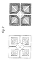
- an etched pattern 2' is shown on the metallised side of the tag (left hand portion of the Figure), and an etched pattern 3' is shown on the opposite (bulk metal) side of the tag (right hand portion of the Figure).
- the tag also commonly termed a label
- the tag is typically 40 mm square.
- the area 4 constitutes an external capacitor
- a fusible link 6 is defined by an etched pattern (as shown) on the metallised side of the tag.
- the fusible link 6 connects the external capacitor 4 with the areas 7, which constitute an internal capacitor.
- the metallised areas 8 constitute a coil. This preferably has eight turns, each preferably 0.8 mm wide on 1 mm in pitch.
- Slits 9 are present in the positions indicated in order to reduce eddy current losses in the capacitor plates, which are typically 0.2 mm thick. Note that the slits of opposing capacitor plates cross approximately at right angles in this embodiment, minimising capacitance errors from any misregistration of etch patterns.
- the presently preferred route for manufacturing the RF tags of this invention is based on well established material processing techniques using readily available starting materials.
- the following Examples illustrate these techniques:
- This Example illustrates the production of a tag having a metallised pattern generally as shown in Figure 2.
- the preferred starting material is a composite web of aluminium foil laminated to metallised polypropylene (as shown in Figure 1). This gives a lower loss polymer dielectric layer twenty microns thick, with twenty microns of aluminium on the bulk metal side, and 0.05 microns of aluminium on the other (metallised) side.
- the web is simultaneously printed on both sides with the required etch resist patterns in a gravure cylinder printing process. Registration holes are inserted into the edges of the web at this stage to provide proper location of the film at the label stamping stage (see below).
- the resist is then dried and the web fed through the acid based etchant bath to generate the desired metallisation patterns.
- the completed circuit is then neutralised and dried; the etch resist may not have to be removed.
- polyester as the polymer layer: this has higher dielectric loss than polypropylene, but has the advantage that aluminium/polyester laminate is readily available.
- glue bonding or direct hot nip of the polymer to the aluminium, is possible.
- the major concern with both techniques is to produce a consistent and uniform dielectric thickness with good bonding between the layers. If a glue layer is used its thickness should be minimised (one micron ideally), as it represents a higher loss portion of the dielectric.
- the present invention permits the following features to be incorporated into the processing or tag fabrication steps:
- FIG. 4 A different label structure in accordance with this invention has also been produced, where aluminium/polyester laminate is etched into coils, and subsequently laminated to a polypropylene layer which has previously been metallised in strips.
- This forms a coil capacitor circuit with the polypropylene as the dielectric, and the metallised strips forming the capacitors and current return path.
- Figures 4 and 5 of the drawings Figures 4a and 5a show the 'coil' side of the tag, while Figures 5a and 5b show the strip capacitors on the opposite side of the tag.
- the arrangements of Figures 4 and 5 differ in their geometries, as shown.
- the polypropylene dielectric 41 is eight microns thick and carries strips of metallised aluminium coating 42 which (in this embodiment) are 6mm wide.
- the resistivity is 0.5 ohms/square mm.
- a similar polypropylene dielectric carries a diagonally disposed strip 52 of metallised aluminium coating which incorporates laser cuts 61a, 61b etc. which constitute a fusible link between portions of the metallised strip; when subjected to a high RF field swept through the resonant frequency of the circuit, these links fuse, thereby deactivating the tag.
- An alternative construction is shown in Figure 5c, where different geometries of fusible metallised areas are depicted.
- FIG. 5d The overall lamination is illustrated in Figure 5d, where a top layer 70 approximately 40 microns thick is secured over the aluminium coil 53, which is approximately 25 microns thick; this is over the polypropylene dielectric layer 51 (eight microns thick); and the metallised, strip-form zones 61 are carried by layer 51.
- the metallised strips 61 are approximately 70nm thick.
- the mode of implementation illustrated in Figures 4 and 5 has the advantage that the polymer layer can be obtained metallised in stripes at low cost, and needs no further processing after it has been laminated to the coil.
Landscapes
- Physics & Mathematics (AREA)
- Automation & Control Theory (AREA)
- Computer Security & Cryptography (AREA)
- Electromagnetism (AREA)
- General Physics & Mathematics (AREA)
- Engineering & Computer Science (AREA)
- Burglar Alarm Systems (AREA)
- Materials For Medical Uses (AREA)
- Cosmetics (AREA)
- Absorbent Articles And Supports Therefor (AREA)
- Confectionery (AREA)
- Medicinal Preparation (AREA)
- Adornments (AREA)
- ing And Chemical Polishing (AREA)
- Fixed Capacitors And Capacitor Manufacturing Machines (AREA)
- Pharmaceuticals Containing Other Organic And Inorganic Compounds (AREA)
- Dental Preparations (AREA)
- Compositions Of Macromolecular Compounds (AREA)
- Adhesives Or Adhesive Processes (AREA)
- Magnetic Resonance Imaging Apparatus (AREA)
- Making Paper Articles (AREA)
Abstract
Description
- This invention relates to antipilferage markers of the type traditionally referred to as radiofrequency (RF) tags. These tags typically use a capacitor-inductor combination to provide a circuit having a characteristic electromagnetic resonance which, in use, receives an RF signal in an interrogation zone and, in response thereto, transmits a signal, e.g. to a receiver in order to generate an alarm indication. This invention is particularly concerned with a novel means for fabricating the tag circuit.
- The general operation and certain methods of assembly of such RF tags are disclosed in patents such as those of Lichtblau (US 3810247, US 3863244, US 3967161, US 4021705). In order to construct the appropriate circuit elements, two or more layers of metal are required. In the prior art this has been achieved by the exclusive use of metal foils of substantial thickness (typically several microns or several tens of microns) which are normally manufactured by rolling techniques. The foils are usually cut, slit, or etched into complex shapes, and are often folded to form the two layers. For example, U.S. Patent No. 4,910,499 (S. Eugene Benge, assigned to Monarch Marking Systems, Inc.) discloses a deactivatable tag useable with an electronic article surveillance system and which comprises a pair of spiral conductive elements which are mutually inverse in their orientation. The spirals are formed by a cutting process. The disadvantages of the prior art processes are in the amount of metal required, and in the complex patterns and alignments which are needed in manufacture.
- According to one aspect of the present invention, there is provided a tag which includes a resonant circuit adapted to receive an RF signal and to transmit a response signal when interrogated by said RF signal, characterised in that at least a part of the tag is constituted by, or is formed from, a precursor comprising a polymer dielectric having a thin, metallised coating less than 1 micron thick on one surface thereof. Advantageously, the precursor comprises a polymer dielectric carrying the thin, metallised coating on one surface thereof and a bulk metal layer on the opposite surface thereof.
- According to a second aspect, the present invention provides an antipilferage tag which includes a resonant circuit adapted to receive an RF signal and to transmit a response signal when interrogated by said RF signal, characterised in that the tag includes circuit components constituted by or fabricated from a metallised layer less than 1 micron thick supported by a dielectric material.
- Typically, the present invention enables one or more layers of metallisation to be used to replace one or more of the normal metal layers. The use of a metallised layer as part of the RF tag circuit gives many potential advantages over the prior art. For example, it may permit lower-cost construction, involving fewer laminated layers; it may permit the easier formation of a fusible link for tag deactivation; it may allow the production of a more flexible label for application to goods; and it may permit a number of manufacturing simplifications which (for example) may reduce the amount of dissolved metal and hence the quantity of chemicals used if an etching process is being employed.
- The metallised layer used in this invention may be formed by a number of conventional methods. They include evaporation, sputtering, chemical or vapour deposition, and electroplating. The material metallised may be any suitable metal, but copper and (more preferably) aluminium have optimal properties. The metallisation will be typically less than 1 micron thick; in the preferred embodiment it is as thin as 0.1 micron.
- Additional features that can be incorporated into the tag of the present invention include the breaking up of the area of the capacitor electrodes (especially on the side of the tag where thick metal is used, i.e. on the coil side of the tag) to reduce losses from eddy currents. Appropriate features to accomplish this effect are illustrated by Figure 2, and may be incorporated into the mask pattern if the tag is formed by etching.
- The use of a two-capacitor circuit (for example 4 and 7 as shown in Figure 2, and described in greater detail hereinafter) to avoid a metallic through-connection between the two metal layers of the tag is particularly preferred, as it is difficult to form reliable connections to the metallised layer in the conventional stamping process. The two capacitors need not be of equal area; a more efficient use of area results if the outer capacitor is smaller than the inner one, as this gives a larger effective area for the coil on a given sized tag. To avoid any contribution to resonant frequency uncertainty from small misalignments in the upper and lower metal patterns, the capacitor plates are advantageously slightly smaller on one side of the tag than the other, such that the overlapping area does not vary for small displacements.
- Tags which are to be used in electronic article surveillance systems need to have the capacity to be deactivated, so that their signal generating function can be disabled by authorised personnel, e.g. at a goods check-out station. The deactivation process preferably employed in tags of the present invention is to cause a narrow region of the metallised film to go into open circuit under a sufficiently high level of RF field swept through the resonant frequency. This can be achieved by conventional means. The use of the metallised layer as the deactivating means a represents novel variation on the prior art technique of fusing part of the coil, and permits low cross section structures that blow under reasonable field levels to be easily defined. Accordingly, in another aspect, the present invention provides an antipilferage tag which includes a resonant circuit adapted to receive an RF signal and to transmit a response signal when interrogated by said RF signal, characterised in that the tag includes deactivating means in the form of a circuit component constituted by or fabricated from a metallised layer less than 1 micron thick supported by a dielectric material.
- The deactivation field can be reduced if a narrower neck is formed in the metallisation pattern, but any large improvement would be at the expense of increased resistive losses and hence reduced Q. Thicker metallisation may be deposited in areas other than the fusing zone to reduce the overall resistivity; this may be achieved, for example, by electrodeposition, a further evaporation process, or electroless plating.
- Lower field deactivation can be promoted without increasing resistive losses by keeping the fusible area under mechanical stress, in a similar way to that in which fast blow fuses incorporate a spring. This provides more consistent fusing at lower field strengths. This can be incorporated at manufacture by embossing the area surrounding the fusible link. This is significantly different from the technique disclosed in US 4,498,076 (Lichtblau, 1985), which refers to mechanically enhanced short circuiting of the tag capacitor rather than open circuiting of a fuse. Alternatively the stress can be introduced by heating areas of the tag around the fuse during manufacture.
- Other deactivation techniques, such as voltage induced dielectric breakdown between the two metal surfaces, or between different parts of the coil, may also be used if desired.
- The use of a metallised layer as part of the RF tag circuit gives many potential advantages compared with the prior art of using bulk metal, e.g. aluminium, on both sides; for example it may permit lower cost at construction, fewer laminated layers, easy formation of a fusible link for deactivation, less dissolved metal if the coil is etched, less chemical usage and less waste.
- In a further aspect, the invention provides a method of fabricating an antipilferage tag, which method comprises:
- (a) bonding a metal layer to one surface of a laminar dielectric material;
- (b) depositing a thin, metallised coating onto the opposite surface of said dielectric material; and
- (c) generating circuit components from said metal layer and from said thin, metallised coating;
- The invention will now be illustrated, by way of example, with reference to the accompanying drawings, in which:
- FIGURE 1 shows the starting materials for tag production before the circuit has been formed;
- FIGURE 2 shows suitable conductive patterns of metallisation (Fig 2a being those on one side of the tag, while Fig. 2b being those on the opposite side of the tag) and an equivalent circuit diagram (Fig. 2c);
- FIGURE 3 is an example of mask etch patterns; and
- FIGURES 4 and 5 illustrate an alternative tag construction in accordance with this invention.
- Referring now to Figure 1, a polymer dielectric 1, typically 8 to 20 microns thick, and typically a polyester or polypropylene, carries a
metallisation layer 2, typically aluminium 0.1 micron thick. The opposite side of polymer dielectric 1 carries abulk conductor layer 3, typically a 20 micron layer of aluminium. Lamination of thebulk metal 3 to thepolymer 1 is shown at 4; this may be either by an adhesive layer (typically 2 microns thick), or by direct hot nip or extrusion of thepolymer 1 onto thebulk metal foil 3. - Referring next to Figure 2, an etched pattern 2' is shown on the metallised side of the tag (left hand portion of the Figure), and an etched pattern 3' is shown on the opposite (bulk metal) side of the tag (right hand portion of the Figure). The tag (also commonly termed a label) is typically 40 mm square. The
area 4 constitutes an external capacitor, and afusible link 6 is defined by an etched pattern (as shown) on the metallised side of the tag. Thefusible link 6 connects theexternal capacitor 4 with theareas 7, which constitute an internal capacitor. Themetallised areas 8 constitute a coil. This preferably has eight turns, each preferably 0.8 mm wide on 1 mm in pitch.Slits 9 are present in the positions indicated in order to reduce eddy current losses in the capacitor plates, which are typically 0.2 mm thick. Note that the slits of opposing capacitor plates cross approximately at right angles in this embodiment, minimising capacitance errors from any misregistration of etch patterns. - The presently preferred route for manufacturing the RF tags of this invention is based on well established material processing techniques using readily available starting materials. The following Examples illustrate these techniques:
- This Example illustrates the production of a tag having a metallised pattern generally as shown in Figure 2. The preferred starting material is a composite web of aluminium foil laminated to metallised polypropylene (as shown in Figure 1). This gives a lower loss polymer dielectric layer twenty microns thick, with twenty microns of aluminium on the bulk metal side, and 0.05 microns of aluminium on the other (metallised) side.
- The web is simultaneously printed on both sides with the required etch resist patterns in a gravure cylinder printing process. Registration holes are inserted into the edges of the web at this stage to provide proper location of the film at the label stamping stage (see below). The resist is then dried and the web fed through the acid based etchant bath to generate the desired metallisation patterns. The completed circuit is then neutralised and dried; the etch resist may not have to be removed.
- This requires the addition of a paper top layer on one side of the circuit, and pressure sensitive adhesive and release paper on the other, before the labels are stamped out making use of the registration holes put into the circuit at the resist printing stage.
- Use of polyester as the polymer layer: this has higher dielectric loss than polypropylene, but has the advantage that aluminium/polyester laminate is readily available.
- Use of glue bonding, or direct hot nip of the polymer to the aluminium, is possible. The major concern with both techniques is to produce a consistent and uniform dielectric thickness with good bonding between the layers. If a glue layer is used its thickness should be minimised (one micron ideally), as it represents a higher loss portion of the dielectric.
- The present invention permits the following features to be incorporated into the processing or tag fabrication steps:
- A. Optimisation of the basic etching process to minimise cost;
- B. Reduction of the amount of material removed; Leaving resist in place at end of process;
- C. Printing and etching of both sides of the tag simultaneously;
- D. Shot blasting of the aluminium laminate using a rubber compound resist printed onto the foil to define the coil pattern. This technique could also be used to etch the pattern on the metallised side of the plastic; alternatively this pattern could be formed at the evaporation stage using a suitable mask, and then just the coil pattern shot blasted.
- E. Connecting the two aluminium layers together by stamping through the plastic at the outside end of the coil. This saves having capacitor plates at both ends of the coil, but may cause problems if used to connect to an extremely thin evaporated layer of metallised aluminium.
-
- F. The choice of label top surface can be wide, as the active portion of the tag is thin, and hence of low stiffness. The stiffness is also lowered by the etching of the bulk aluminium in order to generate a coil. This should allow for Roboskin, thermal and conventional paper to be used.
- G. Manufacture of traditional shaped edged labels with adjacent rows of labels overlapping minimising waste - the tag etch patterns have to be created in this way to start with.
- A different label structure in accordance with this invention has also been produced, where aluminium/polyester laminate is etched into coils, and subsequently laminated to a polypropylene layer which has previously been metallised in strips. This forms a coil capacitor circuit with the polypropylene as the dielectric, and the metallised strips forming the capacitors and current return path. This structure is illustrated in Figures 4 and 5 of the drawings. Figures 4a and 5a show the 'coil' side of the tag, while Figures 5a and 5b show the strip capacitors on the opposite side of the tag. The arrangements of Figures 4 and 5 differ in their geometries, as shown. In Figure 4b, the polypropylene dielectric 41 is eight microns thick and carries strips of
metallised aluminium coating 42 which (in this embodiment) are 6mm wide. The resistivity is 0.5 ohms/square mm. In Figure 5b, a similar polypropylene dielectric carries a diagonally disposedstrip 52 of metallised aluminium coating which incorporateslaser cuts 61a, 61b etc. which constitute a fusible link between portions of the metallised strip; when subjected to a high RF field swept through the resonant frequency of the circuit, these links fuse, thereby deactivating the tag. An alternative construction is shown in Figure 5c, where different geometries of fusible metallised areas are depicted. The overall lamination is illustrated in Figure 5d, where atop layer 70 approximately 40 microns thick is secured over thealuminium coil 53, which is approximately 25 microns thick; this is over the polypropylene dielectric layer 51 (eight microns thick); and the metallised, strip-form zones 61 are carried bylayer 51. The metallised strips 61 are approximately 70nm thick. - The mode of implementation illustrated in Figures 4 and 5 has the advantage that the polymer layer can be obtained metallised in stripes at low cost, and needs no further processing after it has been laminated to the coil.
Claims (19)
- A tag for use in electronic article surveillance systems, which tag includes a resonant circuit adapted to receive an RF signal and to transmit a response signal when interrogated by said RF signal, characterised in that at least a part of the tag is constituted by, or is formed from, a precursor comprising a polymer dielectric having a thin, metallised coating less than 1 micron thick on one surface thereof.
- An antipilferage tag which includes a resonant circuit adapted to receive an RF signal and to transmit a response signal when interrogated by said RF signal, characterised in that the tag includes circuit components constituted by or fabricated from a metallised layer less than 1 micron thick supported by a dielectric material.
- A tag as claimed in claim 1, characterised in that said precursor comprises a polymer dielectric having a thin, metallised coating less than 1 micron thick on one surface thereof and bulk metallic layer on the opposite surface thereof.
- A tag as claimed in claim 1, 2 or 3, characterised in that said thin, metallised coating is formed by evaporation, sputtering, chemical or vapour deposition, or electroplating.
- A tag as claimed in claim 1, 2, 3 or 4, characterised in that the material which constitutes said thin, metallised coating is copper or aluminium.
- A tag as claimed in claim 5, characterised in that said thin, metallised coating is 0.1 micron in thickness.
- A tag as claimed in any preceding claim, characterised in that it includes a two-capacitor circuit.
- A tag as claimed in claim 7, characterised in that there is an outer capacitor and an inner capacitor.
- A tag as claimed in claim 8, characterised in that the outer capacitor is smaller than the inner one.
- A tag as claimed in claim 7, 8 or 9, characterised in that the capacitor plates are slightly smaller on one side of the tag than the other.
- A tag as claimed in claim 7, 8, 9 or 10, characterised in that said capacitor plates are provided with slits which reduce eddy current losses.
- A tag as claimed in claim 11, wherein the slits in opposed capacitor plates are substantially perpendicular to each other.
- An antipilferage tag which includes a resonant circuit adapted to receive an RF signal and to transmit a response signal when interrogated by said RF signal, characterised in that the tag includes deactivating means in the form of a circuit component constituted by or fabricated from a metallised layer less than 1 micron thick supported by a dielectric material.
- A tag as claimed in any preceding claim, characterised in that the deactivating means is a narrow region of the metallised film which constitutes a fusible link.
- A tag as claimed in claim 14, characterised in that said fusible link is capable of being fused, thereby going into open circuit, when subjected to a sufficiently high level of RF field swept through the resonant frequency of the circuit.
- A tag as claimed in claim 14 or 15 when appendant to claim 7, characterised in that said fusible link is constituted by a conductive path between one of the capacitor plates of said inner capacitor and the adjacent capacitor plate of said outer capacitor.
- A tag as claimed in any preceding claim, characterised in that the tag is formed by bonding together two laminar components, the first being an aluminium/polyester laminate the aluminium of which has been etched into coils; and the second being a polypropylene layer onto which has been deposited thin, metallised strips.
- A method of fabricating an antipilferage tag, which method comprises:(a) bonding a metal layer to one surface of a laminar dielectric material;(b) depositing a thin, metallised coating onto the opposite surface of said dielectric material; and(c) generating circuit components from said metal layer and from said thin, metallised coating;characterised in that said thin, metallised coating is less than 1 micron thick.
- A method according to claim 18, characterised in that said thin, metallised coating is etched to generate the desired circuit geometry.
Applications Claiming Priority (3)
| Application Number | Priority Date | Filing Date | Title |
|---|---|---|---|
| GB91147934 | 1991-07-09 | ||
| GB919114793A GB9114793D0 (en) | 1991-07-09 | 1991-07-09 | Novel rf tag |
| PCT/GB1992/001250 WO1993001571A1 (en) | 1991-07-09 | 1992-07-09 | Antipilferage markers |
Publications (2)
| Publication Number | Publication Date |
|---|---|
| EP0594714A1 EP0594714A1 (en) | 1994-05-04 |
| EP0594714B1 true EP0594714B1 (en) | 1997-11-26 |
Family
ID=10698062
Family Applications (1)
| Application Number | Title | Priority Date | Filing Date |
|---|---|---|---|
| EP92915331A Expired - Lifetime EP0594714B1 (en) | 1991-07-09 | 1992-07-09 | Antipilferage markers |
Country Status (13)
| Country | Link |
|---|---|
| US (1) | US5689263A (en) |
| EP (1) | EP0594714B1 (en) |
| JP (1) | JP2863770B2 (en) |
| AT (1) | ATE160640T1 (en) |
| AU (1) | AU654733B2 (en) |
| BR (1) | BR9206258A (en) |
| CA (1) | CA2113111C (en) |
| DE (1) | DE69223321T2 (en) |
| ES (1) | ES2111074T3 (en) |
| FI (1) | FI112551B (en) |
| GB (1) | GB9114793D0 (en) |
| NO (1) | NO308498B1 (en) |
| WO (1) | WO1993001571A1 (en) |
Families Citing this family (22)
| Publication number | Priority date | Publication date | Assignee | Title |
|---|---|---|---|---|
| US5401584A (en) * | 1993-09-10 | 1995-03-28 | Knogo Corporation | Surveillance marker and method of making same |
| US6343313B1 (en) * | 1996-03-26 | 2002-01-29 | Pixion, Inc. | Computer conferencing system with real-time multipoint, multi-speed, multi-stream scalability |
| NL1002720C2 (en) * | 1996-03-27 | 1997-09-30 | Nedap Nv | Fixed frequency resonance label for theft prevention |
| US6087940A (en) * | 1998-07-28 | 2000-07-11 | Novavision, Inc. | Article surveillance device and method for forming |
| US6091607A (en) * | 1998-12-10 | 2000-07-18 | Checkpoint Systems, Inc. | Resonant tag with a conductive composition closing an electrical circuit |
| DE19908877A1 (en) * | 1999-03-01 | 2000-10-12 | Georg Siegel Gmbh Zur Verwertu | Goods security label for LF operation has flat carrier element with defined number of tracks of electrically conducting material applied to one surface parallel to each other to form spiral path |
| FR2799650B1 (en) | 1999-10-14 | 2001-12-07 | Oreal | PROCESS FOR LIMITING THE PENETRATION IN THE SKIN AND / OR KERATINIC FIBERS OF AN ACTIVE COSMETIC AND / OR PHARMACEUTICAL AGENT |
| FI112288B (en) * | 2000-01-17 | 2003-11-14 | Rafsec Oy | Procedure for producing an input path for smart labels |
| FI112287B (en) * | 2000-03-31 | 2003-11-14 | Rafsec Oy | Procedure for producing product sensor and product sensor |
| FI112121B (en) | 2000-12-11 | 2003-10-31 | Rafsec Oy | Smart label web, process for making the same, method for making a carrier web and construction part for a smart label in a smart label web |
| US6489891B1 (en) * | 2001-05-16 | 2002-12-03 | Sensormatic Electronics Corporation | Apparatus for electronic article surveillance tag pollution reduction |
| FI112550B (en) | 2001-05-31 | 2003-12-15 | Rafsec Oy | Smart label and smart label path |
| FI117331B (en) | 2001-07-04 | 2006-09-15 | Rafsec Oy | Method of manufacturing an injection molded product |
| FR2832530B1 (en) * | 2001-11-22 | 2004-08-20 | Nojim | METHOD FOR MANUFACTURING A LABEL WITH RESONANCE CIRCUITS |
| FI119401B (en) * | 2001-12-21 | 2008-10-31 | Upm Raflatac Oy | Smart label web and process for its manufacture |
| US20050231372A1 (en) * | 2004-03-30 | 2005-10-20 | Tokyo Electron Limited | Device for remote identification of parts |
| US7327261B2 (en) * | 2005-07-27 | 2008-02-05 | Zih Corp. | Visual identification tag deactivation |
| US20090021377A1 (en) * | 2006-10-19 | 2009-01-22 | Upm Raflatac Oy | Tamperproof tag |
| US8179203B2 (en) * | 2008-10-09 | 2012-05-15 | The United States Of America, As Represented By The Administrator Of The National Aeronautics And Space Administration | Wireless electrical device using open-circuit elements having no electrical connections |
| JP5522250B2 (en) | 2010-02-26 | 2014-06-18 | 株式会社村田製作所 | High frequency dielectric material |
| US8692562B2 (en) | 2011-08-01 | 2014-04-08 | The United States Of America As Represented By The Administrator Of The National Aeronautics And Space Administration | Wireless open-circuit in-plane strain and displacement sensor requiring no electrical connections |
| US9329153B2 (en) | 2013-01-02 | 2016-05-03 | United States Of America As Represented By The Administrator Of The National Aeronautics And Space Administration | Method of mapping anomalies in homogenous material |
Family Cites Families (10)
| Publication number | Priority date | Publication date | Assignee | Title |
|---|---|---|---|---|
| US3863244A (en) * | 1972-06-14 | 1975-01-28 | Lichtblau G J | Electronic security system having improved noise discrimination |
| US3810147A (en) * | 1971-12-30 | 1974-05-07 | G Lichtblau | Electronic security system |
| US3967161A (en) * | 1972-06-14 | 1976-06-29 | Lichtblau G J | A multi-frequency resonant tag circuit for use with an electronic security system having improved noise discrimination |
| US4021705A (en) * | 1975-03-24 | 1977-05-03 | Lichtblau G J | Resonant tag circuits having one or more fusible links |
| US4498076A (en) * | 1982-05-10 | 1985-02-05 | Lichtblau G J | Resonant tag and deactivator for use in an electronic security system |
| US4910499A (en) * | 1986-09-29 | 1990-03-20 | Monarch Marking Systems, Inc. | Tag and method of making same |
| US4835524A (en) * | 1987-12-17 | 1989-05-30 | Checkpoint System, Inc. | Deactivatable security tag |
| US5006856A (en) * | 1989-08-23 | 1991-04-09 | Monarch Marking Systems, Inc. | Electronic article surveillance tag and method of deactivating tags |
| US5059950A (en) * | 1990-09-04 | 1991-10-22 | Monarch Marking Systems, Inc. | Deactivatable electronic article surveillance tags, tag webs and method of making tag webs |
| US5494550A (en) * | 1993-09-07 | 1996-02-27 | Sensormatic Electronics Corporation | Methods for the making of electronic article surveillance tags and improved electronic article surveillance tags produced thereby |
-
1991
- 1991-07-09 GB GB919114793A patent/GB9114793D0/en active Pending
-
1992
- 1992-07-09 AT AT92915331T patent/ATE160640T1/en not_active IP Right Cessation
- 1992-07-09 EP EP92915331A patent/EP0594714B1/en not_active Expired - Lifetime
- 1992-07-09 BR BR9206258A patent/BR9206258A/en not_active IP Right Cessation
- 1992-07-09 WO PCT/GB1992/001250 patent/WO1993001571A1/en not_active Ceased
- 1992-07-09 ES ES92915331T patent/ES2111074T3/en not_active Expired - Lifetime
- 1992-07-09 DE DE69223321T patent/DE69223321T2/en not_active Expired - Fee Related
- 1992-07-09 AU AU22628/92A patent/AU654733B2/en not_active Ceased
- 1992-07-09 CA CA002113111A patent/CA2113111C/en not_active Expired - Fee Related
- 1992-07-09 JP JP5502110A patent/JP2863770B2/en not_active Expired - Fee Related
-
1994
- 1994-01-06 NO NO940055A patent/NO308498B1/en not_active IP Right Cessation
- 1994-01-07 US US08/178,571 patent/US5689263A/en not_active Expired - Fee Related
- 1994-01-07 FI FI940070A patent/FI112551B/en not_active IP Right Cessation
Also Published As
| Publication number | Publication date |
|---|---|
| US5689263A (en) | 1997-11-18 |
| CA2113111A1 (en) | 1993-01-21 |
| NO940055L (en) | 1994-01-06 |
| ES2111074T3 (en) | 1998-03-01 |
| FI940070L (en) | 1994-01-07 |
| ATE160640T1 (en) | 1997-12-15 |
| GB9114793D0 (en) | 1991-08-28 |
| DE69223321T2 (en) | 1998-08-27 |
| FI112551B (en) | 2003-12-15 |
| WO1993001571A1 (en) | 1993-01-21 |
| EP0594714A1 (en) | 1994-05-04 |
| BR9206258A (en) | 1995-08-08 |
| AU2262892A (en) | 1993-02-11 |
| JP2863770B2 (en) | 1999-03-03 |
| AU654733B2 (en) | 1994-11-17 |
| DE69223321D1 (en) | 1998-01-08 |
| JPH07504280A (en) | 1995-05-11 |
| NO308498B1 (en) | 2000-09-18 |
| NO940055D0 (en) | 1994-01-06 |
| FI940070A0 (en) | 1994-01-07 |
| CA2113111C (en) | 2000-01-11 |
Similar Documents
| Publication | Publication Date | Title |
|---|---|---|
| AU654733B2 (en) | Antipilferage markers | |
| EP1952316B1 (en) | Capacitor strap | |
| EP0203083B1 (en) | Folded rf marker for electronic article surveillance systems | |
| US4583099A (en) | Resonant tag circuits useful in electronic security systems | |
| US5108822A (en) | Resonant tag and method of manufacturing the same | |
| DE69518261T2 (en) | Resonance labels and manufacturing processes | |
| US6835412B2 (en) | Metalized dielectric substrates for EAS tags | |
| EP1051885A1 (en) | Thin film transferable electric components | |
| JPH04245597A (en) | Tag for monitoring article | |
| US7113131B2 (en) | Metalized dielectric substrates for EAS tags | |
| US20020171528A1 (en) | Process for producing resonant tag | |
| US20020050929A1 (en) | Deactivatable electronic article surveillance tag and method for making same | |
| US20010044013A1 (en) | Thin film transferrable electric components | |
| EP1233370A1 (en) | Method of manufacturing resonant circuits | |
| US6198393B1 (en) | Foil/ink composite inductor | |
| JP2002260924A (en) | Foil / ink composite coil and method of forming the same |
Legal Events
| Date | Code | Title | Description |
|---|---|---|---|
| PUAI | Public reference made under article 153(3) epc to a published international application that has entered the european phase |
Free format text: ORIGINAL CODE: 0009012 |
|
| 17P | Request for examination filed |
Effective date: 19940203 |
|
| AK | Designated contracting states |
Kind code of ref document: A1 Designated state(s): AT BE CH DE DK ES FR GB IT LI NL SE |
|
| GRAG | Despatch of communication of intention to grant |
Free format text: ORIGINAL CODE: EPIDOS AGRA |
|
| GRAH | Despatch of communication of intention to grant a patent |
Free format text: ORIGINAL CODE: EPIDOS IGRA |
|
| 17Q | First examination report despatched |
Effective date: 19970411 |
|
| GRAH | Despatch of communication of intention to grant a patent |
Free format text: ORIGINAL CODE: EPIDOS IGRA |
|
| GRAA | (expected) grant |
Free format text: ORIGINAL CODE: 0009210 |
|
| AK | Designated contracting states |
Kind code of ref document: B1 Designated state(s): AT BE CH DE DK ES FR GB IT LI NL SE |
|
| PG25 | Lapsed in a contracting state [announced via postgrant information from national office to epo] |
Ref country code: LI Free format text: LAPSE BECAUSE OF FAILURE TO SUBMIT A TRANSLATION OF THE DESCRIPTION OR TO PAY THE FEE WITHIN THE PRESCRIBED TIME-LIMIT Effective date: 19971126 Ref country code: IT Free format text: LAPSE BECAUSE OF FAILURE TO SUBMIT A TRANSLATION OF THE DESCRIPTION OR TO PAY THE FEE WITHIN THE PRE;WARNING: LAPSES OF ITALIAN PATENTS WITH EFFECTIVE DATE BEFORE 2007 MAY HAVE OCCURRED AT ANY TIME BEFORE 2007. THE CORRECT EFFECTIVE DATE MAY BE DIFFERENT FROM THE ONE RECORDED.SCRIBED TIME-LIMIT Effective date: 19971126 Ref country code: DK Free format text: LAPSE BECAUSE OF NON-PAYMENT OF DUE FEES Effective date: 19971126 Ref country code: CH Free format text: LAPSE BECAUSE OF FAILURE TO SUBMIT A TRANSLATION OF THE DESCRIPTION OR TO PAY THE FEE WITHIN THE PRESCRIBED TIME-LIMIT Effective date: 19971126 Ref country code: AT Free format text: LAPSE BECAUSE OF FAILURE TO SUBMIT A TRANSLATION OF THE DESCRIPTION OR TO PAY THE FEE WITHIN THE PRESCRIBED TIME-LIMIT Effective date: 19971126 |
|
| REF | Corresponds to: |
Ref document number: 160640 Country of ref document: AT Date of ref document: 19971215 Kind code of ref document: T |
|
| REG | Reference to a national code |
Ref country code: CH Ref legal event code: EP |
|
| REF | Corresponds to: |
Ref document number: 69223321 Country of ref document: DE Date of ref document: 19980108 |
|
| ET | Fr: translation filed | ||
| PG25 | Lapsed in a contracting state [announced via postgrant information from national office to epo] |
Ref country code: SE Free format text: LAPSE BECAUSE OF FAILURE TO SUBMIT A TRANSLATION OF THE DESCRIPTION OR TO PAY THE FEE WITHIN THE PRESCRIBED TIME-LIMIT Effective date: 19980226 |
|
| REG | Reference to a national code |
Ref country code: ES Ref legal event code: FG2A Ref document number: 2111074 Country of ref document: ES Kind code of ref document: T3 |
|
| REG | Reference to a national code |
Ref country code: CH Ref legal event code: PL |
|
| PLBE | No opposition filed within time limit |
Free format text: ORIGINAL CODE: 0009261 |
|
| STAA | Information on the status of an ep patent application or granted ep patent |
Free format text: STATUS: NO OPPOSITION FILED WITHIN TIME LIMIT |
|
| 26N | No opposition filed | ||
| REG | Reference to a national code |
Ref country code: GB Ref legal event code: IF02 |
|
| PGFP | Annual fee paid to national office [announced via postgrant information from national office to epo] |
Ref country code: DE Payment date: 20041216 Year of fee payment: 13 |
|
| PGFP | Annual fee paid to national office [announced via postgrant information from national office to epo] |
Ref country code: ES Payment date: 20041230 Year of fee payment: 13 |
|
| PGFP | Annual fee paid to national office [announced via postgrant information from national office to epo] |
Ref country code: NL Payment date: 20050629 Year of fee payment: 14 |
|
| PGFP | Annual fee paid to national office [announced via postgrant information from national office to epo] |
Ref country code: GB Payment date: 20050706 Year of fee payment: 14 |
|
| PG25 | Lapsed in a contracting state [announced via postgrant information from national office to epo] |
Ref country code: ES Free format text: LAPSE BECAUSE OF NON-PAYMENT OF DUE FEES Effective date: 20050711 |
|
| PGFP | Annual fee paid to national office [announced via postgrant information from national office to epo] |
Ref country code: FR Payment date: 20050718 Year of fee payment: 14 |
|
| PGFP | Annual fee paid to national office [announced via postgrant information from national office to epo] |
Ref country code: BE Payment date: 20050819 Year of fee payment: 14 |
|
| PG25 | Lapsed in a contracting state [announced via postgrant information from national office to epo] |
Ref country code: DE Free format text: LAPSE BECAUSE OF NON-PAYMENT OF DUE FEES Effective date: 20060201 |
|
| PG25 | Lapsed in a contracting state [announced via postgrant information from national office to epo] |
Ref country code: GB Free format text: LAPSE BECAUSE OF NON-PAYMENT OF DUE FEES Effective date: 20060709 |
|
| PG25 | Lapsed in a contracting state [announced via postgrant information from national office to epo] |
Ref country code: BE Free format text: LAPSE BECAUSE OF NON-PAYMENT OF DUE FEES Effective date: 20060731 |
|
| REG | Reference to a national code |
Ref country code: ES Ref legal event code: FD2A Effective date: 20050711 |
|
| PG25 | Lapsed in a contracting state [announced via postgrant information from national office to epo] |
Ref country code: NL Free format text: LAPSE BECAUSE OF NON-PAYMENT OF DUE FEES Effective date: 20070201 |
|
| GBPC | Gb: european patent ceased through non-payment of renewal fee |
Effective date: 20060709 |
|
| NLV4 | Nl: lapsed or anulled due to non-payment of the annual fee |
Effective date: 20070201 |
|
| REG | Reference to a national code |
Ref country code: FR Ref legal event code: ST Effective date: 20070330 |
|
| BERE | Be: lapsed |
Owner name: *ESSELTE METO INTERNATIONAL G.M.B.H. Effective date: 20060731 |
|
| PG25 | Lapsed in a contracting state [announced via postgrant information from national office to epo] |
Ref country code: FR Free format text: LAPSE BECAUSE OF NON-PAYMENT OF DUE FEES Effective date: 20060731 |