EP0594049B1 - Insulated gate bipolar transistor and manufacturing method thereof - Google Patents
Insulated gate bipolar transistor and manufacturing method thereof Download PDFInfo
- Publication number
- EP0594049B1 EP0594049B1 EP93116565A EP93116565A EP0594049B1 EP 0594049 B1 EP0594049 B1 EP 0594049B1 EP 93116565 A EP93116565 A EP 93116565A EP 93116565 A EP93116565 A EP 93116565A EP 0594049 B1 EP0594049 B1 EP 0594049B1
- Authority
- EP
- European Patent Office
- Prior art keywords
- semiconductor region
- semiconductor
- region
- type semiconductor
- conductivity type
- Prior art date
- Legal status (The legal status is an assumption and is not a legal conclusion. Google has not performed a legal analysis and makes no representation as to the accuracy of the status listed.)
- Expired - Lifetime
Links
- 238000004519 manufacturing process Methods 0.000 title claims description 44
- 239000004065 semiconductor Substances 0.000 claims description 443
- 239000012535 impurity Substances 0.000 claims description 78
- 238000000034 method Methods 0.000 claims description 32
- 239000000758 substrate Substances 0.000 description 23
- 239000010408 film Substances 0.000 description 14
- 238000004088 simulation Methods 0.000 description 9
- 238000002347 injection Methods 0.000 description 8
- 239000007924 injection Substances 0.000 description 8
- 108091006146 Channels Proteins 0.000 description 7
- XUIMIQQOPSSXEZ-UHFFFAOYSA-N Silicon Chemical compound [Si] XUIMIQQOPSSXEZ-UHFFFAOYSA-N 0.000 description 7
- 230000006378 damage Effects 0.000 description 7
- 238000009413 insulation Methods 0.000 description 7
- 238000000206 photolithography Methods 0.000 description 7
- 230000008569 process Effects 0.000 description 7
- 229910052710 silicon Inorganic materials 0.000 description 7
- 239000010703 silicon Substances 0.000 description 7
- 239000000969 carrier Substances 0.000 description 6
- 229910052782 aluminium Inorganic materials 0.000 description 4
- XAGFODPZIPBFFR-UHFFFAOYSA-N aluminium Chemical compound [Al] XAGFODPZIPBFFR-UHFFFAOYSA-N 0.000 description 4
- 230000015572 biosynthetic process Effects 0.000 description 4
- 230000015556 catabolic process Effects 0.000 description 4
- 238000009792 diffusion process Methods 0.000 description 4
- 229910021420 polycrystalline silicon Inorganic materials 0.000 description 4
- 230000009467 reduction Effects 0.000 description 4
- 230000008859 change Effects 0.000 description 3
- 230000003071 parasitic effect Effects 0.000 description 3
- 229920005591 polysilicon Polymers 0.000 description 3
- 230000004044 response Effects 0.000 description 3
- 102000004129 N-Type Calcium Channels Human genes 0.000 description 2
- 108090000699 N-Type Calcium Channels Proteins 0.000 description 2
- 230000000694 effects Effects 0.000 description 2
- 230000006872 improvement Effects 0.000 description 2
- 229910052751 metal Inorganic materials 0.000 description 2
- 239000002184 metal Substances 0.000 description 2
- 230000001419 dependent effect Effects 0.000 description 1
- 238000011161 development Methods 0.000 description 1
- 230000018109 developmental process Effects 0.000 description 1
- 230000005684 electric field Effects 0.000 description 1
- -1 i.e. Substances 0.000 description 1
- 239000011159 matrix material Substances 0.000 description 1
- 238000012986 modification Methods 0.000 description 1
- 230000004048 modification Effects 0.000 description 1
- 238000002360 preparation method Methods 0.000 description 1
- 230000004224 protection Effects 0.000 description 1
- 239000010409 thin film Substances 0.000 description 1
Images


Classifications
-
- H—ELECTRICITY
- H01—ELECTRIC ELEMENTS
- H01L—SEMICONDUCTOR DEVICES NOT COVERED BY CLASS H10
- H01L29/00—Semiconductor devices adapted for rectifying, amplifying, oscillating or switching, or capacitors or resistors with at least one potential-jump barrier or surface barrier, e.g. PN junction depletion layer or carrier concentration layer; Details of semiconductor bodies or of electrodes thereof ; Multistep manufacturing processes therefor
- H01L29/66—Types of semiconductor device ; Multistep manufacturing processes therefor
- H01L29/66007—Multistep manufacturing processes
- H01L29/66075—Multistep manufacturing processes of devices having semiconductor bodies comprising group 14 or group 13/15 materials
- H01L29/66227—Multistep manufacturing processes of devices having semiconductor bodies comprising group 14 or group 13/15 materials the devices being controllable only by the electric current supplied or the electric potential applied, to an electrode which does not carry the current to be rectified, amplified or switched, e.g. three-terminal devices
- H01L29/66234—Bipolar junction transistors [BJT]
- H01L29/66325—Bipolar junction transistors [BJT] controlled by field-effect, e.g. insulated gate bipolar transistors [IGBT]
- H01L29/66333—Vertical insulated gate bipolar transistors
-
- H—ELECTRICITY
- H01—ELECTRIC ELEMENTS
- H01L—SEMICONDUCTOR DEVICES NOT COVERED BY CLASS H10
- H01L29/00—Semiconductor devices adapted for rectifying, amplifying, oscillating or switching, or capacitors or resistors with at least one potential-jump barrier or surface barrier, e.g. PN junction depletion layer or carrier concentration layer; Details of semiconductor bodies or of electrodes thereof ; Multistep manufacturing processes therefor
- H01L29/02—Semiconductor bodies ; Multistep manufacturing processes therefor
- H01L29/06—Semiconductor bodies ; Multistep manufacturing processes therefor characterised by their shape; characterised by the shapes, relative sizes, or dispositions of the semiconductor regions ; characterised by the concentration or distribution of impurities within semiconductor regions
- H01L29/08—Semiconductor bodies ; Multistep manufacturing processes therefor characterised by their shape; characterised by the shapes, relative sizes, or dispositions of the semiconductor regions ; characterised by the concentration or distribution of impurities within semiconductor regions with semiconductor regions connected to an electrode carrying current to be rectified, amplified or switched and such electrode being part of a semiconductor device which comprises three or more electrodes
- H01L29/083—Anode or cathode regions of thyristors or gated bipolar-mode devices
- H01L29/0834—Anode regions of thyristors or gated bipolar-mode devices, e.g. supplementary regions surrounding anode regions
-
- H—ELECTRICITY
- H01—ELECTRIC ELEMENTS
- H01L—SEMICONDUCTOR DEVICES NOT COVERED BY CLASS H10
- H01L29/00—Semiconductor devices adapted for rectifying, amplifying, oscillating or switching, or capacitors or resistors with at least one potential-jump barrier or surface barrier, e.g. PN junction depletion layer or carrier concentration layer; Details of semiconductor bodies or of electrodes thereof ; Multistep manufacturing processes therefor
- H01L29/66—Types of semiconductor device ; Multistep manufacturing processes therefor
- H01L29/66007—Multistep manufacturing processes
- H01L29/66075—Multistep manufacturing processes of devices having semiconductor bodies comprising group 14 or group 13/15 materials
- H01L29/66227—Multistep manufacturing processes of devices having semiconductor bodies comprising group 14 or group 13/15 materials the devices being controllable only by the electric current supplied or the electric potential applied, to an electrode which does not carry the current to be rectified, amplified or switched, e.g. three-terminal devices
- H01L29/66234—Bipolar junction transistors [BJT]
- H01L29/66325—Bipolar junction transistors [BJT] controlled by field-effect, e.g. insulated gate bipolar transistors [IGBT]
- H01L29/66333—Vertical insulated gate bipolar transistors
- H01L29/66348—Vertical insulated gate bipolar transistors with a recessed gate
-
- H—ELECTRICITY
- H01—ELECTRIC ELEMENTS
- H01L—SEMICONDUCTOR DEVICES NOT COVERED BY CLASS H10
- H01L29/00—Semiconductor devices adapted for rectifying, amplifying, oscillating or switching, or capacitors or resistors with at least one potential-jump barrier or surface barrier, e.g. PN junction depletion layer or carrier concentration layer; Details of semiconductor bodies or of electrodes thereof ; Multistep manufacturing processes therefor
- H01L29/66—Types of semiconductor device ; Multistep manufacturing processes therefor
- H01L29/68—Types of semiconductor device ; Multistep manufacturing processes therefor controllable by only the electric current supplied, or only the electric potential applied, to an electrode which does not carry the current to be rectified, amplified or switched
- H01L29/70—Bipolar devices
- H01L29/72—Transistor-type devices, i.e. able to continuously respond to applied control signals
- H01L29/739—Transistor-type devices, i.e. able to continuously respond to applied control signals controlled by field-effect, e.g. bipolar static induction transistors [BSIT]
- H01L29/7393—Insulated gate bipolar mode transistors, i.e. IGBT; IGT; COMFET
- H01L29/7395—Vertical transistors, e.g. vertical IGBT
- H01L29/7396—Vertical transistors, e.g. vertical IGBT with a non planar surface, e.g. with a non planar gate or with a trench or recess or pillar in the surface of the emitter, base or collector region for improving current density or short circuiting the emitter and base regions
- H01L29/7397—Vertical transistors, e.g. vertical IGBT with a non planar surface, e.g. with a non planar gate or with a trench or recess or pillar in the surface of the emitter, base or collector region for improving current density or short circuiting the emitter and base regions and a gate structure lying on a slanted or vertical surface or formed in a groove, e.g. trench gate IGBT
-
- H—ELECTRICITY
- H01—ELECTRIC ELEMENTS
- H01L—SEMICONDUCTOR DEVICES NOT COVERED BY CLASS H10
- H01L21/00—Processes or apparatus adapted for the manufacture or treatment of semiconductor or solid state devices or of parts thereof
- H01L21/02—Manufacture or treatment of semiconductor devices or of parts thereof
- H01L21/04—Manufacture or treatment of semiconductor devices or of parts thereof the devices having at least one potential-jump barrier or surface barrier, e.g. PN junction, depletion layer or carrier concentration layer
- H01L21/18—Manufacture or treatment of semiconductor devices or of parts thereof the devices having at least one potential-jump barrier or surface barrier, e.g. PN junction, depletion layer or carrier concentration layer the devices having semiconductor bodies comprising elements of Group IV of the Periodic System or AIIIBV compounds with or without impurities, e.g. doping materials
- H01L21/185—Joining of semiconductor bodies for junction formation
- H01L21/187—Joining of semiconductor bodies for junction formation by direct bonding
Definitions
- the present invention relates to an insulated gate semiconductor device such as an insulated gate bipolar transistor (hereinafter abbreviated as "IGBT") and a method of manufacturing the same.
- IGBT insulated gate bipolar transistor
- An insulated gate bipolar transistor is a semiconductor device which has a structure in which p-type semiconductor regions and n-type semiconductor regions are joined so that at least four semiconductor regions of alternate conductivity type are disposed in series.
- the two outer semiconductor regions at least, are electrically connected to a positive and a negative main electrodes, respectively.
- a gate electrode for applying an electric field is connected to one of the two inner semiconductor regions.
- a current which flows between the two main electrodes changes in accordance with a voltage which is applied to the gate electrode.
- An IGBT, an EST (Emitter Switched Thyristor), a MCT (MOS Controlled Thyristor) and the like fall within this category of semiconductor device.
- Fig. 20 is a cross sectional view showing the structure of a conventional N-channel type IGBT.
- an IGBT is comprised of a number of IGBT elements (hereinafter "unit cells") which are connected parallel to each other.
- Fig. 20 shows a cross section of one unit cell.
- an n-type semiconductor layer 11 is formed on a p-type semiconductor layer 1 which includes a p-type semiconductor substrate, whereby a semiconductor substrate body 12 is formed.
- a p-type base region 4 is formed by selective diffusion of p-type impurities.
- an n-type emitter region 5 is formed by selective diffusion of n-type impurities.
- a gate insulation film 7 is disposed on top surface of the p-type base region 4 between the top surface of the n-type semiconductor layer 11 and the top major surface of the n-type emitter region 5.
- a gate electrode 8 which is made of polycrystalline silicon (hereinafter simply as "polysilicon") is formed on the gate insulation film 7, a gate electrode 8 which is made of polycrystalline silicon (hereinafter simply as "polysilicon”) is formed.
- An emitter electrode 9 made of aluminum is disposed in electrical connection to both the p-type base region 4 and the n-type emitter region 5.
- the gate electrode 8 and the emitter electrode 9 are insulated from each other.
- the gate electrodes 8 of the respective unit cells are electrically connected with each other and the emitter electrodes 9 of the respective unit cells are also electrically connected with each other.
- a collector electrode 10 which is made of metal such as aluminum is electrically connected to the bottom major surface of the p-type semiconductor layer 1.
- the collector electrodes 10 of the respective unit cells are contiguous with each other.
- the n-type semiconductor layer 11 includes a buffer layer 2 which is heavily doped n-type where it abuts the p-type semiconductor layer 1.
- the n-type semiconductor layer 3 excluding the buffer layer 2 has an impurity concentration of about 10 14 cm -3 (In general, the withstand voltage becomes higher in proportion to decrease of the impurity concentration. The following description will be made for the IGBT having a withstand voltage class of 600V.)
- the concentration of n-type impurities is about 10 17 cm -3 .
- a predetermined collector voltage V CE is applied between the emitter electrode 9 and the collector electrode 10. If in addition to this, a gate voltage V GE exceeding a threshold value which the device inherently has is applied between the emitter electrode 9 and the gate electrode 8, the p-type base region 4 is inverted into the n-type at a channel region 6 which is located in the vicinity of the gate electrode 8, thereby creating an n-type channel at the channel region 6. Through this channel, carriers, in this case electrons, are introduced from the emitter electrode 9 into the n-type semiconductor layer 3.
- a forward bias is applied between the p-type semiconductor layer 1 and the n-type semiconductor layer 11, causing injection of carriers, i.e., holes in this case, from the p-type semiconductor layer 1.
- the resistance of the p-type semiconductor layer 1 drops largely so that a collector current I C flowing from the collector electrode 10 to the emitter electrode 9 drastically increases.
- the device turns conductive (i.e., turns on).
- a resistance against the collector current I C at such an occasion is called an ON-resistance.
- the ON-resistance is in most cases expressed as the collector voltage V CE when the collector current I C is equal to a normal rated current value (i.e., saturation collector voltage V CE (sat)).
- the normal rated current of the conventional IGBT is typically around 50 to 150 A/cm 2 .
- the resistance of the n-type semiconductor layer 11 is reduced by means of injection of holes from the p-type semiconductor layer 1.
- Fig. 21 is a graph showing output characteristics of the device in response to various gate voltages V GE .
- the collector voltage V CE is increased while the gate voltage V GE of a certain value is applied, the flow rate of electrons flowing in the channel is suppressed by a certain amount which corresponds to the gate voltage V GE .
- the collector current I C flowing in the device saturates at a constant value which corresponds to the gate voltage V GE , that is, at a saturation collector current I C (sat) (horizontal straight portions of the curves in Fig. 21).
- the buffer layer 2 controls injection of holes from the p-type semiconductor layer 1.
- holes from the p-type semiconductor layer 1 easily combine with electrons which exist in the buffer layer 2.
- provision of the buffer layer 2 lowers the saturation collector current I C (sat) while enhances the ON-resistance.
- the saturation collector current I C (sat) and the ON-resistance can be adjusted.
- the collector voltage V CE is increased under OFF-state of the device by means of a reduction in the gate voltage V GE to zero or other suitable method, the collector current I C would not be started until the collector voltage V CE reaches a certain value. However, once the collector voltage V CE has grown beyond the certain value, the collector current I C will start flowing and become increasingly large.
- the collector voltage V CE at this stage is referred to as "breakdown voltage.”
- the collector voltage V CE which can be applied to the IGBT is less than the breakdown voltage.
- the IGBT includes a parasitic thyristor which is formed by the n-type emitter region 5, the p-type base region 4, the n-type semiconductor layer 11 and the p-type semiconductor layer 1.
- the parasitic thyristor turns on if the collector current I C exceeds a certain value (i.e., latch up current) (Ts is known as "latching up of the IGBT").
- latch up current Ts is known as "latching up of the IGBT"
- the buffer layer 2 is formed having a thickness which would allow injection of holes from the p-type semiconductor layer 1 in a great number in order to reduce the ON-resistance, the value of the saturation collector current I C (sat) which is developed in response to application of a certain gate voltage V GE would increase. If the saturation collector current I C (sat) is large, the collector current I C tends to exceed the latch up current during the operations of the IGBT. The result of this is an increased possibility of destruction of the IGBT due to latch up.
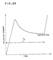
- Fig. 22 is a graph showing the waveform of the collector current I C with a change in time after the short circuiting. Immediately after the short circuiting, the collector current I C exhibits an abrupt increase, amounting to a maximum value which is about 5 to 20 times as large as the normal rated current value (50 to 150 A/cm 2 ). It is when the collector current I C is at this maximum level that the IGBT is most likely to be destroyed due to latch up.
- the collector current I C After the collector current I C reached the maximum level, even if latch up has not occurred, a continued unusually large collector current I C far beyond a normal level under normal environment is still observed. Due to this, the IGBT will be destroyed after a certain time Tv.
- the time Tv during which the IGBT remains undestroyed though short circuiting, must be longer than 10 to 20 ⁇ sec for practical reasons. In the art, it is a general knowledge that the lower the collector current I C is during short circuiting of the device, the longer the time Tv is.
- the collector current I C during short circuiting is defined at a value of the saturation collector current I C (sat).
- the value of the saturation collector current I C (sat) in response to application of a. certain gate voltage V GE would increase. If the saturation collector current I C (sat) is large, the collector current I C under short circuiting becomes large, and therefore, the time Tv becomes short.
- the conventional IGBT has a drawback that a low ON-resistance easily causes destruction of the IGBT due to latch up and subsequent short circuiting (short-circuit destruction).
- an insulated gate semiconductor device wherein a first semiconductor region of a first conductivity type, a second semiconductor region of a second conductivity type formed on the first semiconductor region, a third semiconductor region of the first conductivity type selectively formed on the second semiconductor region, a fourth semiconductor region of the second conductivity type formed on the third semiconductor region and a fifth semiconductor region of the second conductivity type formed in the bottom portion of the second semiconductor region is known.
- the third, fourth and fifth semiconductor regions comprise gaps.
- An insulating layer for a control electrode as well as first and second main electrodes are provided.
- MOSFET is known wherein the conductivity may be modulated.
- the MOSFET comprises semiconductor regions in the substrate opposite to the active regions.
- insulated gate type bipolar transistors with overvoltage protections are known wherein in the substrate partial doped semiconductor regions are provided for the transistor.
- the insulated gate semiconductor device In the insulated gate semiconductor device according to the present invention, injection of carriers from the first semiconductor region to the second semiconductor region is attained by carriers which selectively flow in a region where the fifth semiconductor region is not present.
- a current which flows between the first and the second main electrodes is small, under a predominant influence of a fact that the carrier concentration at such a region is higher than where the device does not comprise the fifth semiconductor region, flow of the current is facilitated. In other words, the ON-resistance of the device becomes lower than that where the fifth semiconductor region is not provided.
- the first portion of the second semiconductor region prevents a depletion region which grows from the third semiconductor region from reaching the first semiconductor region. Hence, even if the second semiconductor region is thin, there is no possibility that punch through will be caused.
- the impurity concentrations of the second conductivity type in the first, second, and the fifth semiconductor regions are optimized. Hence, a reduction in the ON-resistance and an improvement in the breakdown voltage are better achieved in the device.
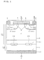
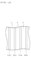
- Fig. 1 is a cross sectional view showing the structure of an insulated gate semiconductor device according to a first example.
- the illustrated device is an IGBT of a withstand voltage class of 600V.
- the IGBT of the first preferred embodiment has a structure in which a number of unit cells are connected in parallel with each other.
- Fig. 1 shows a cross section of one unit cell.
- elements or parts corresponding to the same or equivalent elements are denoted by the same reference numerals.
- an n-type semiconductor layer 11 is formed on a p-type semiconductor layer 1 which includes a p-type semiconductor substrate, whereby a semiconductor substrate body 12 is formed.
- a p-type base region 4 is formed by selective diffusion of p-type impurities.
- the base region 4 comprises first and second portions 4a and 4b in the section illustrated in Fig. 1, portions 4a and 4b being separated from each other.
- an n-type emitter region 5 is formed by selective diffusion of n-type impurities.
- a region outside the p-type base region 4 and the n-type emitter region 5 are isolated from each other by the p-type base region 4.
- the emitter region 5 comprises first and second portions 5a and 5b in the section illustrated in Fig. 1.
- a gate insulation film 7 i.e., insulating layer
- a gate electrode 8 which is made of polysilicon (i.e., control electrode layer), for example, is formed facing the top surface of p-type base region 4.
- An emitter electrode 9 made of aluminum (second main electrode layer) is disposed in electrical connection to both the p-type base region 4 and the n-type emitter region 5. The gate electrode 8 and the emitter electrode 9 are insulated from each other.
- the gate electrodes 8 of the respective unit cells are electrically connected with each other and the emitter electrodes 9 of the respective unit cells are also electrically connected with each other.
- a collector electrode 10 which is made of metal such as aluminum (first main electrode layer) is electrically connected to the bottom major surface of the p-type semiconductor layer 1.
- the collector electrodes 10 of the respective unit cells are contiguous with each other.
- the n-type semiconductor layer 11 includes a buffer layer 21 which is heavily doped n-type where it abuts the p-type semiconductor layer 1.
- the n-type semiconductor layer 3 excluding the buffer layer 21 has a relatively low impurity concentration equal to or less than about 5 ⁇ 10 14 cm -3 , for example.
- the concentration of n-type impurities is in the range between approximately 5 ⁇ 10 14 cm -3 and 10 17 cm -3 .
- the buffer layer 21 and the p-type semiconductor layer 1 still other semiconductor regions, i.e., heavily doped n-type semiconductor region 22 is selectively formed.
- the impurity concentration of the heavily doped n-type semiconductor region 22 is in the range between approximately 10 18 cm -3 and 10 21 cm -3 , a concentration equal to or more than about 100 times as high as that of the buffer layer 21.
- a predetermined collector voltage V CE is applied between the emitter electrode 9 and the collector electrode 10. If in addition to this a gate voltage V GE exceeding the inherent threshold value of the MOS device formed by elements 40, 46, 7 and the portion of element 3 between 40 and 46 is applied between the emitter electrode 9 and the gate electrode 8, carriers, holes in this case, migrate from the p-type semiconductor layer 1 to the n-type semiconductor layer 11. As a result, the IGBT turns on, or in other words, the collector current I C flows from the collector electrode 10 to the emitter electrode 9.
- the saturation collector current I C (sat) is smaller and the ON-resistance is higher as compared with those of where the buffer layer 21 is not provided.
- the IGBT turns off, thereby no collector current I C flows.
- the buffer layer 21 prevents punch through due to growth of a depletion layer from the p-type base region 4 to the p-type semiconductor layer 1 during the device OFF-state, which feature being also shared by the buffer layer 2 of the conventional device. Therefore, reduction in the thickness of the n-type semiconductor layer 3 is possible, allowing significant economies in production. In addition, the thin n-type semiconductor layer 3 reduces the turn-off time of the device.
- the buffer layer 21, which has a relatively low concentration of the n-type impurities, and the n-type semiconductor region 22, which has a relatively high concentration of the n-type impurities, are arranged parallel with each other between the n-type semiconductor layer 3 and the p-type semiconductor layer 1. That is, a region which does not easily allow holes to flow from the p-type semiconductor layer 1 into the n-type semiconductor layer 3 is located parallel to a region which relatively easily allows holes to flow from the p-type semiconductor layer 1 into the n-type semiconductor layer 3.
- Injection of holes from the p-type semiconductor layer 1 into the n-type semiconductor layer 3 when the collector current I C is small is achieved by selective passage of holes at a region where the heavily doped n-type semiconductor region 22 does not exist.
- the collector current I C flows through selected region of buffer layer 21 where the heavily doped n-type semiconductor region 22 is not provided.
- the injection of the holes is dominant, so that the ON-resistance of the device is comparable with a device where the heavily doped n-type semiconductor region 22 is not provided.
- the collector current I C is large, under an overwhelmingly strong influence of a fact that the collector current I C is allowed to flow through only the region where the heavily doped n-type semiconductor regions 22 are not provided, flow of the collector current I C will be suppressed. That is, when the collector current I C is large, the collector current I C is lower than it would be if the device does not include the heavily doped n-type semiconductor region 22. Thus, the durability against destruction of the device is improved.
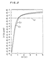
- Fig. 2 is a graph showing simulation data which are compiled to illustrate the improvements possible with the device of the invention.
- Figs. 3A and 3B are cross sectional views showing the structures of model semiconductor devices used in the simulation.
- the well known PISCES2B simulation (PISCES2B is a registered trademark) was utilized.
- the diode comprises the p-type semiconductor layer 1, the buffer layer 21, the heavily doped n-type semiconductor region 22 and the n-type semiconductor layer 3, each having a thickness shown in Fig. 3A (typical thicknesses shown for example only).
- the heavily doped n-type semiconductor region 22 is disposed over a width x which is equal to a width y over which the heavily doped n-type semiconductor region 22 is not provided.
- the n-type impurities are doped to the range between 5 ⁇ 10 14 cm -3 and 10 17 cm -3 within the buffer layer 21 and to the range between 10 18 cm -3 and 10 21 cm -3 within the heavily doped n-type semiconductor region 22.
- FIG. 3B Another model is a diode which corresponds to a portion of the conventional IGBT (Fig. 3B).
- the model of Fig. 3B is different from the model of Fig. 3A in that the heavily doped n-type semiconductor region 22 is omitted.
- the concentration of the n-type impurities of the buffer layer 2 is set at around 10 17 cm -3 .
- an extremely thin n-type semiconductor layer 23 of a high impurity concentration is formed on the n-type semiconductor layer 3.
- a forward current I F in each model diode is measured along the vertical axis of the graph and a forward voltage V F in each model diode is measured along the horizontal axis of the graph.
- the forward current I F and the forward voltage V F respectively correspond to the collector current I C and the collector voltage V CE .
- Curves labelled C1 and C2 represent the simulation results of the diodes of Figs. 3A and 3B, respectively.
- a straight line L 1 denotes a current density of 100 A/cm 2 which corresponds to the collector current I C of the IGBT under normal environment.
- Fig. 2 shows that, as compared with the curve C2, the curve C1 indicates a relatively smaller forward voltage V F in a region where the forward current I F is small. In a region where the forward current I F is large, the curve C1 indicates a smaller forward current IF than that indicated by the curve C2 against the same forward voltage V F .
- the IGBT of the first example has a lower ON-resistance in the small forward current region and, in the large forward current region, the collector current I C is smaller against the same forward voltage V F .
- the ON-current of the device is set the same as that of the conventional device for the same normal rated current (i.e., 50 to 150 A/cm 2 )
- a substantially larger reduction in the collector current I C is possible in the large forward current region as compared with that in the conventional device.
- the durability against destruction of the device is extremely enhanced.
- the value of the collector current I C in the large forward current region is same as that of the conventional device, the current capacity around the normal rated current is increased and the ON-resistance is suppressed drastically low.
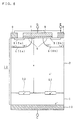
- Fig. 4 is a cross sectional view showing the structure of an IGBT according to a second example.
- the device is different from the device of Fig. 1 in that the buffer layer 21 is thinner than the heavily doped n-type semiconductor region 22 and the buffer layer 21 is not formed on the top surface of the heavily doped n-type semiconductor region 22.
- the second example is similar to the first example.
- the buffer layer 21 of a relatively low n-type impurity concentration or alternatively the heavily doped n-type semiconductor region 22 exists between the n-type semiconductor layer 3 and the p-type semiconductor layer 1. Hence, during the device OFF-state, punch through due to growth of a depletion layer from the p-type base region 4 to the p-type semiconductor layer 1 is prevented by the buffer layer 21 or alternatively the heavily doped n-type semiconductor region 22.
- the buffer layer 21 which is relatively lightly doped n-type and the n-type semiconductor region 22, which is doped n-type heavier than the buffer layer 21 are arranged parallel with each other between the n-type semiconductor layer 3 and the p-type semiconductor layer 1. Hence, holes from the p-type semiconductor layer 1 pass through the n-type semiconductor layer 11 at a selected region (layer 21).
- the device of the second example has a lower ON-resistance than that of the conventional device.
- the collector current I C in the large forward current region is suppressed lower than that in the conventional device.
- the device when designed so that the ON-resistance is equal to that of the conventional device, the device has a further lower collector current I C in the large forward current region as compared with that in the conventional device. Further, by setting the value of the collector current I C in the large forward current region the same as that of the conventional device, the current capacity around the normal rated current of the second preferred embodiment is increased and the ON-resistance is suppressed even lower as compared with the conventional device.
- Fig. 5 is a cross sectional view showing the structure of an IGBT according to a third example.
- the device is different from the device of Fig. 1 in that the heavily doped n-type semiconductor region 22 is selectively formed between the n-type semiconductor layer 3 and the buffer layer 21.
- the third example is similar to the first example.
- the buffer layer 21 of a relatively high n-type impurity concentration or alternatively the heavily doped n-type semiconductor region 22 exists between the n-type semiconductor layer 3 and the p-type semiconductor layer 1. Hence, during the device OFF-state, punch through due to growth of a depletion layer from the p-type base region 4 to the p-type semiconductor layer 1 is prevented by the buffer layer 21 or alternatively the heavily doped n-type semiconductor region 22.
- the device of the third example has a structure in which the buffer layer 21 which is relatively lightly doped n-type and the n-type semiconductor region 22 which is relatively heavily doped n-type are arranged parallel with each other between the n-type semiconductor layer 3 and the p-type semiconductor layer 1. This reduces the ON-resistance and the collector current I C in the large forward current region lower than those in the conventional device. In addition, if the device is designed so as to have an ON-resistance which is equal to that of the conventional device, a further lower collector current I C in the large forward current region than that in the conventional device is attained.
- the current capacity around the normal rated current of the third preferred embodiment is increased and the ON-resistance is suppressed even lower as compared with the conventional device.
- Fig. 6 is a cross sectional view showing the structure of an IGBT according to a fourth example. Omission of the buffer layer 21 is a difference between the device and the device shown in Fig. 1.
- the heavily doped n-type semiconductor region 22 is selectively disposed between the n-type semiconductor layer 3 and the p-type semiconductor layer 1.
- the n-type semiconductor layer 3 and the heavily doped n-type semiconductor region 22 respectively have the same n-type impurity concentrations as those of the equivalent layer and region of the first example.
- the n-type semiconductor layer 3 and the p-type semiconductor layer 1 are directly joined to each other without an interposed heavily doped n-type semiconductor layer.
- the n-type semiconductor layer 3 is formed to have a sufficiently large thickness z.
- the n-type semiconductor layer 3 which is relatively lightly doped n-type and the n-type semiconductor region 22 which is relatively heavily doped n-type are arranged parallel with each other on the top surface of the p-type semiconductor layer 1. This reduces the ON-resistance and the collector current I C in the large forward current region lower than those in the conventional device.
- the device is designed so as to have an ON-voltage which is equal to that of the conventional device, a further lower collector current I C in the large forward current region than that in the conventional device is attained.
- the value of the collector current I C in the large forward current region the same as that of the conventional device, the current capacity around the normal rated current is increased and the ON-resistance is suppressed even lower as compared with the conventional device.
- Fig. 7 is a cross sectional view showing the structure of an IGBT according to a fifth example.
- the device is different from the device of the first example in terms of the structure of an upper portion of the n-type semiconductor layer 3.
- the device of the fifth example known as an U-type IGBT is advantageous over the devices of the preceding examples since it can be formed denser in an easy manner.
- the p-type base region 4 can be formed on the entire top major surface of the n-type semiconductor layer 11 during fabrication and therefore there is no need for selectively forming the p-type base region 4, manufacturing of the device is less complex.
- the p-type base region 4 and the n-type emitter region 5 are formed in the top surface of the n-type semiconductor layer 3.
- a groove 31 is also formed in the top surface of the n-type semiconductor layer 3 so that the side walls of the groove 31 extend across the n-type emitter region 5, the p-type base region 4 and into the n-type semiconductor layer 3.
- a gate insulation film 32 (insulating layer) is disposed.
- a gate electrode 33 made of polysilicon (control electrode layer) is buried inside the insulation film 32.
- the device of the fifth example is similar to the devices of the preceding examples in that the gate electrode 33 is disposed facing the surface of the p-type base region 4.
- the p-type base region 4 With application of the gate voltage V GE of a predetermined value, the p-type base region 4 is inverted into the n-type at a channel region 35 which is formed in the vicinity of the gate electrode 33, creating an n-type channel at the channel region 35.
- Carriers in this case electrons, are introduced from the emitter electrode 9 into the n-type semiconductor layer 3 through this channel, thereby turning on the device. That is, the device of the fifth operates in a way similar to the device of the first example. In terms of the ranges of concentration of the n-type impurities in the buffer layer 21 and the heavily doped n-type semiconductor region 22, the fifth example is similar to the first example.
- the buffer layer 21 of a relatively low n-type impurity concentration and the n-type semiconductor region 22 of a relatively high n-type impurity concentration are arranged parallel with each other between the n-type semiconductor layer 3 and the p-type semiconductor layer 1.
- the ON-resistance and the collector current I C in the large forward current region are suppressed to be low.
- the device of the fifth example is designed so as to have an ON-current which is equal to that of the conventional device, a further lower collector current I C in the large forward current region than that in the conventional device is attained.
- the collector current I C in the large forward current region the same as that of the conventional device, the current capacity around the normal rated current of the fifth example is increased and the ON-resistance is suppressed even lower as compared with the conventional device.
- Fig. 8 is a cross sectional view showing the structure of the IGBT according to a sixth example of the present invention.
- the heavily doped n-type semiconductor region 22 is formed in a different configuration from that of the device of the first example. As shown in Fig. 1, the heavily doped n-type semiconductor region 22 is formed as two portions which are spaced apart from each other in one unit cell. In this this example, however, the heavily doped n-type semiconductor region 22a is formed as one integrated portion in one unit cell.
- the heavily doped n-type semiconductor region is disposed as a continued region right below approximately the whole p-type base region 4 to have a gap right below the n-type semiconductor layer which separates the two portions 4a and 4b of the p-type base region 4.
- the device of this example also functions as the device of the first example and has similar effects.
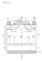
- Fig. 9 is a cross sectional perspective view showing the structure of the IGBT according to a preferred embodiment of the present invention.
- the heavily doped n-type semiconductor region 22 is disposed in a different direction from the heavily doped n-type semiconductor region 22 of the device of the first example.
- the p-type base region 4 formed in the shape of stripes in the top major surface of the n-type semiconductor layer 11 runs parallel to the heavily doped n-type semiconductor region 22 which is also formed in the shape of stripes.
- the heavily doped n-type semiconductor region 22b runs perpendicular to the p-type base region 4.
- the p-type base region 4 and the heavily doped n-type semiconductor region 22 are parallel to each other, a positional relation between the gaps of the heavily doped n-type semiconductor region 22 and the gaps of the p-type base region 4 affects the characteristics of the device. To deal with this, the positional relation must be adjusted accurately if not very strictly accurately. In the device of the invention, however, since the heavily doped n-type semiconductor region 22b and the p-type base region 4 are disposed in intersecting directions, a positional relation between the two can be decided with no restriction. This eliminates the necessity of accurately aligning the mask pattern for formation of the heavily doped n-type semiconductor region 22 during fabrication of the device, which makes the fabrication simple. In addition, the characteristics of the device would not vary among products.
- Fig. 9 shows an example where the p-type base region 4 and the heavily doped n-type semiconductor region 22b run perpendicular to each other, as far as being disposed in directions which cross each other with a certain angle, the same effects are attainable.
- Figs. 10 to 12 are plan views of three different configurations each in the interface between the p-type semiconductor layer 1 and the n-type semiconductor layer 11.
- Fig. 10 shows the configuration of the heavily doped n-type semiconductor region 22 in the preferred embodiment of Fig. 9, namely, the heavily doped n-type semiconductor region 22b which are in the form of parallel stripes.
- the heavily doped n-type semiconductor region 22 of Fig. 1 and the like has a similar configuration.
- the heavily doped n-type semiconductor region 22a shown in Fig. 8 is in a similar configuration, the width and the pitch of the stripes are different.
- the heavily doped n-type semiconductor region 22c shown in Fig. 11 includes a plurality of small square regions which are arranged with a space from each other in a matrix.
- the small regions may not be square.
- the heavily doped n-type semiconductor region 22d shown in Fig. 12 is somewhat similar to the heavily doped n-type semiconductor region 22c and the p-type semiconductor layer 1 of Fig. 11 replaced to each other.
- the heavily doped n-type semiconductor region 22d is in the form of a lattice or cross stripes which includes square openings. The openings may not be square.
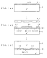
- Figs. 13A to 13C are cross sectional views showing the device of Fig. 1 during successive stages of fabrication.
- a first step of manufacturing the device of the first preferred embodiment is preparation of a p-type silicon substrate which corresponds to the p-type collector layer 1 (Fig. 13A).
- the p-type collector layer 1 is covered at the entire top major surface with a resist layer from which a resist pattern 51 (shielding film) will be subsequently formed by a photolithography process through a mask 61.
- n-type impurities such as As are selectively implanted through the pattern 51, thereby defining an n-type semiconductor region 41 in the top surface of the p-type semiconductor layer 1 (Fig. 21B).
- the buffer layer 21 is then epitaxially grown on the p-type semiconductor layer 1, in the course of which the n-type impurities of the n-type semiconductor region 41 diffuse outside to thereby define the heavily doped n-type semiconductor region 22 between the buffer layer 21 and the p-type semiconductor layer 1.
- the n-type semiconductor layer 3 is then epitaxially grown on the buffer layer 21 (Fig. 21C).
- the device is hereinafter manufactured using conventional processing techniques. More particularly, the top surface of the n-type semiconductor layer 3 is locally doped to form the p-type base region 4 and the n-type emitter region 5 thereat. Then, the gate insulation film 7, the gate electrode 8 and the emitter electrode 9 are connected. Further, the collector electrode 10 is connected to the bottom major surface of the p-type semiconductor layer 1 (Fig. 1).
- Figs. 14A to 14C are cross sectional views showing the device of Fig. 4 during successive stages of fabrication.
- a p-type silicon substrate which corresponds to the p-type collector layer 1 is prepared.
- the buffer layer 21 is formed on the p-type collector layer 1 by epitaxial growth.
- the buffer layer 21 is formed to a thickness which does not exceed the thickness of the heavily doped n-type semiconductor region 22 which will be formed later (Fig. 14A).
- a resist layer is then formed entirely over the top major surface of the p-type collector layer 1 and patterned through a mask 62 by a photolithography process to thereby define a resist pattern 52 (shielding film).
- n-type impurities such as As are selectively implanted through the resist pattern 52, thereby defining an n-type semiconductor region 42 in the top surface of the buffer layer 21 (Fig. 14B).
- the resist pattern 52 is then removed, followed by epitaxial growth of the n-type semiconductor layer 3 on the buffer layer 21.
- the n-type impurities of the n-type semiconductor region 42 diffuse into the n-type semiconductor layer 3 and p-type collector layer 1 while the layer 3 is epitaxially grown so that the heavily doped n-type semiconductor region 22 is formed between the n-type semiconductor layer 3 and the p-type semiconductor layer 1 (Fig. 14C).
- the device shown in Fig. 4 is hereinafter completed by procedures similar to those used to fabricate the device of the first example.
- Figs. 15A to 15C are cross sectional views showing the device of Fig. 5 during successive stages of fabrication.
- a p-type silicon substrate which corresponds to the p-type collector layer 1 is prepared.
- the buffer layer 21 is formed on the p-type collector layer 1 by epitaxial growth.
- the buffer layer 21 is formed to a thickness which is sufficiently larger than the thickness of the heavily doped n-type semiconductor region 22 which will be formed later (Fig. 15A).
- the buffer layer 21 is covered at the entire top major surface with a resist layer from which a resist pattern 53 (shielding film) will be subsequently formed by a photolithography process through a mask 63.
- n-type impurities such as As are selectively implanted through the resist pattern 53, thereby defining an n-type semiconductor region 43 in the top surface of the buffer layer 21 (Fig. 15B).
- the resist pattern 53 is then removed, followed by epitaxial growth of the n-type semiconductor layer 3 on the buffer layer 21.
- the n-type impurities of the n-type semiconductor region 43 diffuse into the n-type semiconductor layer 3 and the buffer layer 21 while the layer is epitaxially grown so that the heavily doped n-type semiconductor region 22 is formed between the n-type semiconductor layer 3 and the buffer layer 21 (Fig. 15C).
- the device shown in Fig. 5 is hereinafter completed by procedures similar to those used to fabricate the device of the first example.
- Figs. 16A to 16C are cross sectional views showing the device of Fig. 6 during successive stages of fabrication. It is to be noted that Figs. 16A to 16C illustrate the device upside down to as it regularly is during fabrication so as to be in conformity with Fig. 6 which shows a cross section of the finished device.
- n-type impurities such as As are selectively implanted through the resist pattern 54, thereby defining an n-type semiconductor region 44 in the bottom surface of the n-type semiconductor layer 3 (Fig. 16B).
- the resist pattern 54 is then removed, and the p-type semiconductor layer 1 is epitaxially grown on the bottom major surface of the n-type semiconductor layer 3.
- the n-type impurities of the n-type semiconductor region 44 diffuse, whereby the heavily doped n-type semiconductor region 22 is formed between the n-type semiconductor layer 3 and the p-type semiconductor layer 1 (Fig. 16C).
- the device shown in Fig. 6 will be hereinafter completed by procedures similar to those used to fabricate the device of the first example.
- the semiconductor substrate which corresponds to the n-type semiconductor layer 3 is prepared first instead of forming the p-type semiconductor layer 1 as in the preceding methods is because the n-type semiconductor layer 3 must be sufficiently thick to manufacture the device of the fourth example. In other words, formation of the n-type semiconductor layer 3 by expensive epitaxial growth contradicts economies in production. Of course, if economies in production is not an important consideration, the p-type semiconductor layer 1 may be prepared first and the n-type semiconductor layer 3 may be formed by epitaxial growth to manufacture the device shown in Fig. 6.
- Fabrication of the device of the fifth example is similar to that explained as the fourth example up to formation of the heavily doped n-type semiconductor region 22.
- the procedures that follow are similar to procedures conventionally used in fabrication of a U-type IGBT.
- the devices according to the first to the third and the fifth examples are also obtainable by preparing the n-type semiconductor layer 3 first instead of the p-type semiconductor layer 1, which is similar to the manufacturing process of the fourth example. In the following such a manufacturing method will be described.
- Figs. 17A to 17C are views showing the device of the first example (Fig. 1) during successive stages of other type of fabrication. Like Figs. 16A to 16C, Figs. 17A to 17C illustrate the device upside down to as it regularly is during fabrication so as to be in conformity with Fig. 1 which shows a cross section of the finished device. For the sake of convenience, Figs. 17A to 17C will be referred to here. This is also the same regarding Figs. 18A to 18C and Figs. 19A to 19C.
- an n-type silicon substrate which corresponds to the n-type semiconductor layer 3 is prepared first.
- the buffer layer 21 is epitaxially grown.
- the buffer layer 21 is formed so as to be sufficiently thicker than the heavily doped n-type semiconductor region 22 described later (Fig. 17A).
- a resist layer is formed all over a bottom major surface of the buffer layer 21 and photolithography patterned using the mask 61, thereby defining the resist pattern 51 (shielding film).
- n-type impurities such as As are selectively injected so that the n-type semiconductor region 41 is selectively formed in the bottom major surface of the buffer layer 21 (Fig. 17B).
- the resist pattern 51 is removed and the p-type semiconductor layer 1 is epitaxially grown on bottom major surface of the buffer layer 21.
- the n-type impurities diffuse from the n-type semiconductor region 41, whereby the heavily doped n-type semiconductor region 22 is formed between the p-type semiconductor layer 1 and the fubber layer 21 (Fig. 17C).
- the impurity concentration of the n-type impurities in the n-type semiconductor layer 3 needs be accurately adjusted, the impurity concentration of the p-type impurities in the p-type semiconductor layer 1 may not be adjusted very accurately.
- the n-type semiconductor layer 3 which requires relatively accurate adjustment is prepared in advance as a substrate and the p-type semiconductor layer 1 which does not require very accurate adjustment is epitaxially grown, and therefore, it is easy to correctly adjust the impurity concentration of the n-type impurities in the n-type semiconductor layer 3.
- the p-type semiconductor layer 1 is formed easily.
- Fig. 18A to 18C are views showing the device of Fig. 4 during successive stages of other type of fabrication.
- this manufacturing method first, an n-type silicon substrate which corresponds to the n-type semiconductor layer 3 is prepared. Next, on a bottom major surface of the n-type semiconductor layer 3, the buffer layer 21 is epitaxially grown. The buffer layer 21 is formed so as to be thinner than the heavily doped n-type semiconductor region 22 described later (Fig. 18A).
- a resist layer is formed all over a bottom major surface of the buffer layer 21 and photolithography patterned using the mask 62, thereby defining the resist pattern 52 (shielding film).
- n-type impurities such as As are selectively injected so that the n-type semiconductor region 42 is selectively formed in the bottom major surface of the buffer layer 21 (Fig. 18B).
- the resist pattern 52 is removed and the p-type semiconductor layer 1 is epitaxially grown on bottom major surface of the buffer layer 21.
- the n-type impurities diffuse from the n-type semiconductor region 42, whereby the heavily doped n-type semiconductor region 22 is formed between the p-type semiconductor layer 1 and the fubber layer 21 (Fig. 18C).
- the device shown in Fig. 4 is fabricated.
- the n-type semiconductor layer 3 which requires relatively accurate adjustment is prepared in advance as a substrate and the p-type semiconductor layer 1 which does not require very accurate adjustment is epitaxially grown, and therefore, it is easy to correctly adjust the impurity concentration of the n-type impurities in the n-type semiconductor layer 3 and to form the p-type semiconductor layer 1.
- Fig. 19A to 19C are views showing the device of Fig. 5 during successive stages of other type of fabrication.
- this manufacturing method first, an n-type silicon substrate which corresponds to the n-type semiconductor layer 3 is prepared (Fig. 19A).
- a resist layer is grown on the entire bottom major surface of the n-type semiconductor layer 3 and photolithography patterned using the mask 63, thereby defining the resist pattern 53 (shielding film).
- n-type impurities such as As are selectively injected so that the n-type semiconductor region 43 is selectively formed in the bottom major surface of the n-type semiconductor layer 3 (Fig. 19B).
- the buffer layer 21 is epitaxially grown on the bottom major surface of the n-type semiconductor layer 3. During this epitaxial growth, the n-type impurities diffuse from the n-type semiconductor region 43, whereby the heavily doped n-type semiconductor region 22 is formed between the buffer layer 21 and the n-type semiconductor layer 3.
- the buffer layer 21 is formed so as to be sufficiently thick so that the heavily doped n-type semiconductor region 22 will not extend to the bottom major surface of the buffer layer 21.
- the p-type semiconductor layer 1 is epitaxially grown on the bottom major surface of the buffer layer 21 (Fig. 19C).
- the device shown in Fig. 5 is obtained.
- the n-type semiconductor layer 3 which requires relatively accurate adjustment is prepared in advance as a substrate and the p-type semiconductor layer 1 which does not require very accurate adjustment is epitaxially grown, and therefore, it is easy to correctly adjust the impurity concentration of the n-type impurities in the n-type semiconductor layer 3 and to form the p-type semiconductor layer 1.
- FIG. 7 Other manufacturing method of the device of Fig. 7 is similar to the processes of Figs. 17A to 17C up to formation of the heavily doped n-type semiconductor region 22.
- the subsequent processes are the same as conventional processes for fabrication of an U-type IGBT.
- the n-type semiconductor layer 3 which requires relatively accurate adjustment is prepared in advance as a substrate and the p-type semiconductor layer 1 which does not require very accurate adjustment is epitaxially grown, and therefore, it is easy to correctly adjust the impurity concentration of the n-type impurities in the n-type semiconductor layer 3 and to form the p-type semiconductor layer 1.
- the present invention is also applicable to a p-channel IGBT in which the semiconductor layers of alternate conductivity are disposed in an opposite manner to that of an n-channel IGBT.
- the present invention can be applied to other types of insulated gate semiconductor devices such as ESTs and MCTs.
Description
- The present invention relates to an insulated gate semiconductor device such as an insulated gate bipolar transistor (hereinafter abbreviated as "IGBT") and a method of manufacturing the same.
- An insulated gate bipolar transistor is a semiconductor device which has a structure in which p-type semiconductor regions and n-type semiconductor regions are joined so that at least four semiconductor regions of alternate conductivity type are disposed in series. The two outer semiconductor regions, at least, are electrically connected to a positive and a negative main electrodes, respectively. To one of the two inner semiconductor regions, a gate electrode for applying an electric field is connected through an insulating thin film. In this type of semiconductor device, a current which flows between the two main electrodes changes in accordance with a voltage which is applied to the gate electrode. An IGBT, an EST (Emitter Switched Thyristor), a MCT (MOS Controlled Thyristor) and the like fall within this category of semiconductor device.
- Fig. 20 is a cross sectional view showing the structure of a conventional N-channel type IGBT. In general, an IGBT is comprised of a number of IGBT elements (hereinafter "unit cells") which are connected parallel to each other. Fig. 20 shows a cross section of one unit cell. In this IGBT, an n-type semiconductor layer 11 is formed on a p-
type semiconductor layer 1 which includes a p-type semiconductor substrate, whereby asemiconductor substrate body 12 is formed. Locally in the top major surface of the n-type semiconductor layer 11, i.e., in the top major surface of thesemiconductor substrate body 12, a p-type base region 4 is formed by selective diffusion of p-type impurities. Also locally in the top major surface of thesemiconductor substrate body 12, an n-type emitter region 5 is formed by selective diffusion of n-type impurities. On top surface of the p-type base region 4 between the top surface of the n-type semiconductor layer 11 and the top major surface of the n-type emitter region 5, agate insulation film 7 is disposed. On thegate insulation film 7, agate electrode 8 which is made of polycrystalline silicon (hereinafter simply as "polysilicon") is formed. - An
emitter electrode 9 made of aluminum is disposed in electrical connection to both the p-type base region 4 and the n-type emitter region 5. Thegate electrode 8 and theemitter electrode 9 are insulated from each other. Thegate electrodes 8 of the respective unit cells are electrically connected with each other and theemitter electrodes 9 of the respective unit cells are also electrically connected with each other. Acollector electrode 10 which is made of metal such as aluminum is electrically connected to the bottom major surface of the p-type semiconductor layer 1. Thecollector electrodes 10 of the respective unit cells are contiguous with each other. - The n-type semiconductor layer 11 includes a
buffer layer 2 which is heavily doped n-type where it abuts the p-type semiconductor layer 1. In the class of IGBT having withstand voltage of 600V, within the n-type semiconductor layer 11, the n-type semiconductor layer 3 excluding thebuffer layer 2 has an impurity concentration of about 1014 cm-3 (In general, the withstand voltage becomes higher in proportion to decrease of the impurity concentration. The following description will be made for the IGBT having a withstand voltage class of 600V.) In thebuffer layer 2, on the other hand, the concentration of n-type impurities is about 1017 cm-3. - Now, the operation of the conventional device will be explained. First, a predetermined collector voltage VCE is applied between the
emitter electrode 9 and thecollector electrode 10. If in addition to this, a gate voltage VGE exceeding a threshold value which the device inherently has is applied between theemitter electrode 9 and thegate electrode 8, the p-type base region 4 is inverted into the n-type at achannel region 6 which is located in the vicinity of thegate electrode 8, thereby creating an n-type channel at thechannel region 6. Through this channel, carriers, in this case electrons, are introduced from theemitter electrode 9 into the n-type semiconductor layer 3. Due to the introduced electrons, a forward bias is applied between the p-type semiconductor layer 1 and the n-type semiconductor layer 11, causing injection of carriers, i.e., holes in this case, from the p-type semiconductor layer 1. As a result, the resistance of the p-type semiconductor layer 1 drops largely so that a collector current IC flowing from thecollector electrode 10 to theemitter electrode 9 drastically increases. In other words, the device turns conductive (i.e., turns on). A resistance against the collector current IC at such an occasion is called an ON-resistance. The ON-resistance is in most cases expressed as the collector voltage VCE when the collector current IC is equal to a normal rated current value (i.e., saturation collector voltage VCE(sat)). The normal rated current of the conventional IGBT is typically around 50 to 150 A/cm2. Thus, in the IGBT, the resistance of the n-type semiconductor layer 11 is reduced by means of injection of holes from the p-type semiconductor layer 1. - Fig. 21 is a graph showing output characteristics of the device in response to various gate voltages VGE. When the collector voltage VCE is increased while the gate voltage VGE of a certain value is applied, the flow rate of electrons flowing in the channel is suppressed by a certain amount which corresponds to the gate voltage VGE. For this reason, the collector current IC flowing in the device saturates at a constant value which corresponds to the gate voltage VGE, that is, at a saturation collector current IC(sat) (horizontal straight portions of the curves in Fig. 21).
- The
buffer layer 2 controls injection of holes from the p-type semiconductor layer 1. In thebuffer layer 2, due to a high concentration of the n-type impurities, holes from the p-type semiconductor layer 1 easily combine with electrons which exist in thebuffer layer 2. Hence, provision of thebuffer layer 2 lowers the saturation collector current IC(sat) while enhances the ON-resistance. By adjusting the thickness and the impurity concentration of thebuffer layer 2, the saturation collector current IC(sat) and the ON-resistance can be adjusted. - If the gate voltage VGE is suppressed under the threshold value while keep applying the collector voltage VCE of a predetermined value, an n-channel would not be created and no collector current IC would be initiated. That is, the IGBT is cut off (i.e., turns off). When the collector voltage VCE is increased under OFF-state of the device by means of a reduction in the gate voltage VGE to zero or other suitable method, the collector current IC would not be started until the collector voltage VCE reaches a certain value. However, once the collector voltage VCE has grown beyond the certain value, the collector current IC will start flowing and become increasingly large. The collector voltage VCE at this stage is referred to as "breakdown voltage." The collector voltage VCE which can be applied to the IGBT is less than the breakdown voltage.
- When the collector voltage VCE as large as about the breakdown voltage is applied to the IGBT, a depletion layer grows from the p-
type base region 4 to as far as thebuffer layer 2. If the depletion layer reaches the p-type semiconductor layer 1, the IGBT turns conductive from the p-type semiconductor layer 1 to the p-type base region 4 (known as "punch through"). Thebuffer layer 2, preventing growth of the depletion layer into the p-type semiconductor layer 1, obviates punch through. - As can be readily understood from the device structure of the IGBT shown in Fig. 20, the IGBT includes a parasitic thyristor which is formed by the n-
type emitter region 5, the p-type base region 4, the n-type semiconductor layer 11 and the p-type semiconductor layer 1. The parasitic thyristor turns on if the collector current IC exceeds a certain value (i.e., latch up current) (Ts is known as "latching up of the IGBT"). Once the parasitic thyristor has turned on, no matter how the gate voltage VGE is controlled, it is impossible to control the collector current IC. The collector current IC then keeps flowing, eventually destroying the IGBT. - If the
buffer layer 2 is formed having a thickness which would allow injection of holes from the p-type semiconductor layer 1 in a great number in order to reduce the ON-resistance, the value of the saturation collector current IC(sat) which is developed in response to application of a certain gate voltage VGE would increase. If the saturation collector current IC(sat) is large, the collector current IC tends to exceed the latch up current during the operations of the IGBT. The result of this is an increased possibility of destruction of the IGBT due to latch up. - Besides, constructed as a switching element, in actual use, the IGBT occasionally turns conductive while a load is short circuited; that is, short circuiting is caused. When the IGBT short circuits, a current flowing in the IGBT is determined by the IGBT alone since there is no load any more which controls the collector current IC. Fig. 22 is a graph showing the waveform of the collector current IC with a change in time after the short circuiting. Immediately after the short circuiting, the collector current IC exhibits an abrupt increase, amounting to a maximum value which is about 5 to 20 times as large as the normal rated current value (50 to 150 A/cm2). It is when the collector current IC is at this maximum level that the IGBT is most likely to be destroyed due to latch up.
- After the collector current IC reached the maximum level, even if latch up has not occurred, a continued unusually large collector current IC far beyond a normal level under normal environment is still observed. Due to this, the IGBT will be destroyed after a certain time Tv. The time Tv, during which the IGBT remains undestroyed though short circuiting, must be longer than 10 to 20 µ sec for practical reasons. In the art, it is a general knowledge that the lower the collector current IC is during short circuiting of the device, the longer the time Tv is. The collector current IC during short circuiting is defined at a value of the saturation collector current IC(sat).
- If injection of an increased number of holes from the p-
type semiconductor layer 1 is allowed by adjusting thebuffer layer 2 to lower the ON-resistance as mentioned above, the value of the saturation collector current IC(sat) in response to application of a. certain gate voltage VGE would increase. If the saturation collector current IC(sat) is large, the collector current IC under short circuiting becomes large, and therefore, the time Tv becomes short. - As heretofore described, the conventional IGBT has a drawback that a low ON-resistance easily causes destruction of the IGBT due to latch up and subsequent short circuiting (short-circuit destruction).
- From JP-A-61-216363 an insulated gate semiconductor device is known wherein a first semiconductor region of a first conductivity type, a second semiconductor region of a second conductivity type formed on the first semiconductor region, a third semiconductor region of the first conductivity type selectively formed on the second semiconductor region, a fourth semiconductor region of the second conductivity type formed on the third semiconductor region and a fifth semiconductor region of the second conductivity type formed in the bottom portion of the second semiconductor region is known. The third, fourth and fifth semiconductor regions comprise gaps. An insulating layer for a control electrode as well as first and second main electrodes are provided.
- From JP-A-2-3288 an insulated gate bipolar transistor is known wherein a groove is formed at the main face of the waver namely in the second, third, and fourth semiconductor regions.
- From DE-A-41 12 905 a MOSFET is known wherein the conductivity may be modulated. The MOSFET comprises semiconductor regions in the substrate opposite to the active regions.
- From EP-A-0 450 082 an insulated gate bipolar transistor is known wherein in the substrate beneath the transistor doped regions are provided.
- From EP-A-0 503 605 insulated gate type bipolar transistors with overvoltage protections are known wherein in the substrate partial doped semiconductor regions are provided for the transistor.
- It is an object of the present invention to obtain an insulated gate semiconductor device having low ON-resistance, and enhanced durability against destruction wherein tolerances for the positions of the individual elements is present.
- Further, a method for manufacturing such devices should be provided.
- Such objects are solved by an insulated gate semiconductor device having the features of the
independent claim 1. - Furthermore, such objects are solved by a method as is claimed in
claims 9 or 14. - Preferred developments of the invention are given in the respective dependent claims.
- In the insulated gate semiconductor device according to the present invention, injection of carriers from the first semiconductor region to the second semiconductor region is attained by carriers which selectively flow in a region where the fifth semiconductor region is not present. As a result, when a current which flows between the first and the second main electrodes is small, under a predominant influence of a fact that the carrier concentration at such a region is higher than where the device does not comprise the fifth semiconductor region, flow of the current is facilitated. In other words, the ON-resistance of the device becomes lower than that where the fifth semiconductor region is not provided.
- On the other hand, if the current is large, under a dominantly strong influence of a fact that flow of the current is allowed only through the region where the fifth semiconductor region is not provided, the flow of the current will be suppressed. Hence, the durability against destruction of the device is improved.
- During the device OFF-state, the first portion of the second semiconductor region prevents a depletion region which grows from the third semiconductor region from reaching the first semiconductor region. Hence, even if the second semiconductor region is thin, there is no possibility that punch through will be caused.
- The impurity concentrations of the second conductivity type in the first, second, and the fifth semiconductor regions are optimized. Hence, a reduction in the ON-resistance and an improvement in the breakdown voltage are better achieved in the device.
- These and other objects, features, aspects and advantages of the present invention will become more apparent from the following detailed description of the present invention when taken in conjunction with the accompanying drawings.
- Fig. 1 is a cross sectional view showing the structure of an insulated gate semiconductor device according to a first example;
- Fig. 2 is a graph showing simulation data which are compiled based on simulation;
- Figs. 3A and 3B are cross sectional views showing the structures of model semiconductor devices used in the simulation shown in Fig. 2;
- Fig. 4 is a cross sectional view showing the structure of an insulated gate semiconductor device according to a second example;
- Fig. 5 is a cross sectional view showing the structure of an insulated gate semiconductor device according to a third example;
- Fig. 6 is a cross sectional view showing the structure of an insulated gate semiconductor device according to a fourth example;
- Fig. 7 is a cross sectional view showing the structure of an insulated gate semiconductor device according to a fifth example;
- Fig. 8 is a cross sectional view showing the structure of an insulated gate semiconductor device according to a sixth example;
- Fig. 9 is a cross sectional view showing the structure of an insulated gate semiconductor device according to a preferred embodiment of the present invention;
- Fig. 10 is a cross sectional view showing the configuration of a heavily doped n-type semiconductor region in the preferred embodiment of the present invention;
- Fig. 11 is a cross sectional view showing the configuration of a heavily doped n-type semiconductor region in another example;
- Fig. 12 is a cross sectional view showing the configuration of a heavily doped n-type semiconductor region in still another example;
- Figs. 13A to 13C are cross sectional views showing the device of the first example during successive stages of fabrication;
- Figs. 14A to 14C are cross sectional views showing the device of the second example during successive stages of fabrication;
- Figs. 15A to 15C are cross sectional views showing the device of the third example during successive stages of fabrication;
- Figs. 16A to 16C are cross sectional views showing the device of the fourth example during successive stages of fabrication;
- Figs. 17A to 17C are cross sectional views showing the device of the first example during successive stages of other type of fabrication;
- Figs. 18A to 18C are cross sectional views showing the device of the second example during successive stages of other type of fabrication;
- Figs. 19A to 19C are cross sectional views showing the device of the third example during successive stages of other type of fabrication;
- Fig. 20 is a cross sectional view showing the structure of a coventional insulated gate semiconductor device;
- Fig. 21 is a graph showing output characteristics of the conventional device; and
- Fig. 22 is a graph showing a change in a collector current with a change in time during short circuiting.
-
- Fig. 1 is a cross sectional view showing the structure of an insulated gate semiconductor device according to a first example. The illustrated device is an IGBT of a withstand voltage class of 600V. Like the conventional IGBT shown in Fig. 20, the IGBT of the first preferred embodiment has a structure in which a number of unit cells are connected in parallel with each other. Fig. 1 shows a cross section of one unit cell. In the drawings hereinafter referred to, elements or parts corresponding to the same or equivalent elements are denoted by the same reference numerals.
- In this IGBT, an n-type semiconductor layer 11 is formed on a p-
type semiconductor layer 1 which includes a p-type semiconductor substrate, whereby asemiconductor substrate body 12 is formed. Locally in the top major surface of the n-type semiconductor layer 11, i.e., in the top major surface of thesemiconductor substrate body 12, a p-type base region 4 is formed by selective diffusion of p-type impurities. Thebase region 4 comprises first andsecond portions portions semiconductor substrate body 12 at a region inside the p-type base region 4, an n-type emitter region 5 is formed by selective diffusion of n-type impurities. In the n-type semiconductor layer 11, a region outside the p-type base region 4 and the n-type emitter region 5 are isolated from each other by the p-type base region 4. Theemitter region 5 comprises first andsecond portions - On the top surface of the p-
type base region 4 between the top surface of the n-type semiconductor layer 11 and the top major surface of the n-type emitter region 5, a gate insulation film 7 (i.e., insulating layer) is disposed. On thegate insulation film 7, agate electrode 8 which is made of polysilicon (i.e., control electrode layer), for example, is formed facing the top surface of p-type base region 4. Anemitter electrode 9 made of aluminum (second main electrode layer) is disposed in electrical connection to both the p-type base region 4 and the n-type emitter region 5. Thegate electrode 8 and theemitter electrode 9 are insulated from each other. Thegate electrodes 8 of the respective unit cells are electrically connected with each other and theemitter electrodes 9 of the respective unit cells are also electrically connected with each other. Acollector electrode 10 which is made of metal such as aluminum (first main electrode layer) is electrically connected to the bottom major surface of the p-type semiconductor layer 1. Thecollector electrodes 10 of the respective unit cells are contiguous with each other. - The n-type semiconductor layer 11 includes a
buffer layer 21 which is heavily doped n-type where it abuts the p-type semiconductor layer 1. Within the n-type semiconductor layer 11, the n-type semiconductor layer 3 excluding thebuffer layer 21 has a relatively low impurity concentration equal to or less than about 5×1014 cm-3, for example. In thebuffer layer 21, the concentration of n-type impurities is in the range between approximately 5×1014 cm-3 and 1017 cm-3. - In addition, at a boundary between the
buffer layer 21 and the p-type semiconductor layer 1, still other semiconductor regions, i.e., heavily doped n-type semiconductor region 22 is selectively formed. The impurity concentration of the heavily doped n-type semiconductor region 22 is in the range between approximately 1018 cm-3 and 1021 cm-3, a concentration equal to or more than about 100 times as high as that of thebuffer layer 21. - The operations of the device according to the first preferred embodiment will now be explained. First, a predetermined collector voltage VCE is applied between the
emitter electrode 9 and thecollector electrode 10. If in addition to this a gate voltage VGE exceeding the inherent threshold value of the MOS device formed byelements 40, 46, 7 and the portion ofelement 3 between 40 and 46 is applied between theemitter electrode 9 and thegate electrode 8, carriers, holes in this case, migrate from the p-type semiconductor layer 1 to the n-type semiconductor layer 11. As a result, the IGBT turns on, or in other words, the collector current IC flows from thecollector electrode 10 to theemitter electrode 9. - Likewise in the
buffer layer 2 of the conventional device, holes introduced from the p-type semiconductor layer 1 easily combine with electrons which exist in the heavily doped n-type buffer layer 21. Hence, in this device which comprises thebuffer layer 21, the saturation collector current IC(sat) is smaller and the ON-resistance is higher as compared with those of where thebuffer layer 21 is not provided. - If the gate voltage VGE is reduced below the threshold value while keeping the collector voltage VCE at a predetermined value, the IGBT turns off, thereby no collector current IC flows. The
buffer layer 21 prevents punch through due to growth of a depletion layer from the p-type base region 4 to the p-type semiconductor layer 1 during the device OFF-state, which feature being also shared by thebuffer layer 2 of the conventional device. Therefore, reduction in the thickness of the n-type semiconductor layer 3 is possible, allowing significant economies in production. In addition, the thin n-type semiconductor layer 3 reduces the turn-off time of the device. - The ON-operation of the device will be described in detail. In this device, the
buffer layer 21, which has a relatively low concentration of the n-type impurities, and the n-type semiconductor region 22, which has a relatively high concentration of the n-type impurities, are arranged parallel with each other between the n-type semiconductor layer 3 and the p-type semiconductor layer 1. That is, a region which does not easily allow holes to flow from the p-type semiconductor layer 1 into the n-type semiconductor layer 3 is located parallel to a region which relatively easily allows holes to flow from the p-type semiconductor layer 1 into the n-type semiconductor layer 3. Injection of holes from the p-type semiconductor layer 1 into the n-type semiconductor layer 3 when the collector current IC is small is achieved by selective passage of holes at a region where the heavily doped n-type semiconductor region 22 does not exist. In other words, the collector current IC flows through selected region ofbuffer layer 21 where the heavily doped n-type semiconductor region 22 is not provided. As a result, when the collector current IC is small, the injection of the holes is dominant, so that the ON-resistance of the device is comparable with a device where the heavily doped n-type semiconductor region 22 is not provided. - On the other hand, if the collector current IC is large, under an overwhelmingly strong influence of a fact that the collector current IC is allowed to flow through only the region where the heavily doped n-
type semiconductor regions 22 are not provided, flow of the collector current IC will be suppressed. That is, when the collector current IC is large, the collector current IC is lower than it would be if the device does not include the heavily doped n-type semiconductor region 22. Thus, the durability against destruction of the device is improved. - Fig. 2 is a graph showing simulation data which are compiled to illustrate the improvements possible with the device of the invention. Figs. 3A and 3B are cross sectional views showing the structures of model semiconductor devices used in the simulation. The well known PISCES2B simulation (PISCES2B is a registered trademark) was utilized.
- As shown in Figs. 3A and 3B, two models were established. One of the two models is a diode which corresponds to a portion of the IGBT of the first preferred embodiment (Fig. 3A). The diode comprises the p-
type semiconductor layer 1, thebuffer layer 21, the heavily doped n-type semiconductor region 22 and the n-type semiconductor layer 3, each having a thickness shown in Fig. 3A (typical thicknesses shown for example only). Between the p-type semiconductor layer 1 and the n-type semiconductor layer 3, the heavily doped n-type semiconductor region 22 is disposed over a width x which is equal to a width y over which the heavily doped n-type semiconductor region 22 is not provided. The n-type impurities are doped to the range between 5×1014 cm-3 and 1017 cm-3 within thebuffer layer 21 and to the range between 1018 cm-3 and 1021 cm-3 within the heavily doped n-type semiconductor region 22. - Another model is a diode which corresponds to a portion of the conventional IGBT (Fig. 3B). The model of Fig. 3B is different from the model of Fig. 3A in that the heavily doped n-
type semiconductor region 22 is omitted. The concentration of the n-type impurities of thebuffer layer 2 is set at around 1017 cm-3. In each model, an extremely thin n-type semiconductor layer 23 of a high impurity concentration is formed on the n-type semiconductor layer 3. - These models each corresponds to a portion of an IGBT and has a structure which allows the determination of the quantity of holes which are injected from the p-
type semiconductor layer 1 and the ON-resistance. By comparing the simulation results of the two models, differences in the structure and operation of the conventional IGBT and the IGBT according to the first example can be evaluated. - In Fig. 2, a forward current IF in each model diode is measured along the vertical axis of the graph and a forward voltage VF in each model diode is measured along the horizontal axis of the graph. The forward current IF and the forward voltage VF respectively correspond to the collector current IC and the collector voltage VCE. Curves labelled C1 and C2 represent the simulation results of the diodes of Figs. 3A and 3B, respectively. A straight line L1 denotes a current density of 100 A/cm2 which corresponds to the collector current IC of the IGBT under normal environment.
- Fig. 2 shows that, as compared with the curve C2, the curve C1 indicates a relatively smaller forward voltage VF in a region where the forward current IF is small. In a region where the forward current IF is large, the curve C1 indicates a smaller forward current IF than that indicated by the curve C2 against the same forward voltage VF. As compared with the conventional IGBT, the IGBT of the first example has a lower ON-resistance in the small forward current region and, in the large forward current region, the collector current IC is smaller against the same forward voltage VF. Thus, the simulation data agree with the description above.
- If the ON-current of the device is set the same as that of the conventional device for the same normal rated current (i.e., 50 to 150 A/cm2), a substantially larger reduction in the collector current IC is possible in the large forward current region as compared with that in the conventional device. In short, the durability against destruction of the device is extremely enhanced. On the other hand, by setting the value of the collector current IC in the large forward current region the same as that of the conventional device, the current capacity around the normal rated current is increased and the ON-resistance is suppressed drastically low.
- Fig. 4 is a cross sectional view showing the structure of an IGBT according to a second example. The device is different from the device of Fig. 1 in that the
buffer layer 21 is thinner than the heavily doped n-type semiconductor region 22 and thebuffer layer 21 is not formed on the top surface of the heavily doped n-type semiconductor region 22. In terms of the ranges of the concentrations of the n-type impurities inf the n-type semiconductor layer 3, thebuffer layer 21 and the heavily doped n-type semiconductor region 22, the second example is similar to the first example. - In the device, the
buffer layer 21 of a relatively low n-type impurity concentration or alternatively the heavily doped n-type semiconductor region 22 exists between the n-type semiconductor layer 3 and the p-type semiconductor layer 1. Hence, during the device OFF-state, punch through due to growth of a depletion layer from the p-type base region 4 to the p-type semiconductor layer 1 is prevented by thebuffer layer 21 or alternatively the heavily doped n-type semiconductor region 22. - In the device of the second example as in the device of the first example, the
buffer layer 21 which is relatively lightly doped n-type and the n-type semiconductor region 22, which is doped n-type heavier than thebuffer layer 21 are arranged parallel with each other between the n-type semiconductor layer 3 and the p-type semiconductor layer 1. Hence, holes from the p-type semiconductor layer 1 pass through the n-type semiconductor layer 11 at a selected region (layer 21). As a result, similar to the device of the first example, the device of the second example has a lower ON-resistance than that of the conventional device. Moreover, the collector current IC in the large forward current region is suppressed lower than that in the conventional device. - In addition, when designed so that the ON-resistance is equal to that of the conventional device, the device has a further lower collector current IC in the large forward current region as compared with that in the conventional device. Further, by setting the value of the collector current IC in the large forward current region the same as that of the conventional device, the current capacity around the normal rated current of the second preferred embodiment is increased and the ON-resistance is suppressed even lower as compared with the conventional device.
- Fig. 5 is a cross sectional view showing the structure of an IGBT according to a third example. The device is different from the device of Fig. 1 in that the heavily doped n-
type semiconductor region 22 is selectively formed between the n-type semiconductor layer 3 and thebuffer layer 21. In terms of the ranges of the concentrations of the n-type impurities in the n-type semiconductor layer 3, thebuffer layer 21 and the heavily doped n-type semiconductor region 22, the third example is similar to the first example. - Also in the device according to the third, the
buffer layer 21 of a relatively high n-type impurity concentration or alternatively the heavily doped n-type semiconductor region 22 exists between the n-type semiconductor layer 3 and the p-type semiconductor layer 1. Hence, during the device OFF-state, punch through due to growth of a depletion layer from the p-type base region 4 to the p-type semiconductor layer 1 is prevented by thebuffer layer 21 or alternatively the heavily doped n-type semiconductor region 22. - Similar to the device of the first example, the device of the third example has a structure in which the
buffer layer 21 which is relatively lightly doped n-type and the n-type semiconductor region 22 which is relatively heavily doped n-type are arranged parallel with each other between the n-type semiconductor layer 3 and the p-type semiconductor layer 1. This reduces the ON-resistance and the collector current IC in the large forward current region lower than those in the conventional device. In addition, if the device is designed so as to have an ON-resistance which is equal to that of the conventional device, a further lower collector current IC in the large forward current region than that in the conventional device is attained. Moreover, by setting the value of the collector current IC in the large forward current region the same as that of the conventional device, the current capacity around the normal rated current of the third preferred embodiment is increased and the ON-resistance is suppressed even lower as compared with the conventional device. - Fig. 6 is a cross sectional view showing the structure of an IGBT according to a fourth example. Omission of the
buffer layer 21 is a difference between the device and the device shown in Fig. 1. The heavily doped n-type semiconductor region 22 is selectively disposed between the n-type semiconductor layer 3 and the p-type semiconductor layer 1. The n-type semiconductor layer 3 and the heavily doped n-type semiconductor region 22 respectively have the same n-type impurity concentrations as those of the equivalent layer and region of the first example. - In the device of the fourth example, where the heavily doped n-
type semiconductor region 21 is not provided, the n-type semiconductor layer 3 and the p-type semiconductor layer 1 are directly joined to each other without an interposed heavily doped n-type semiconductor layer. Hence, to prevent punch through due to growth of a depletion layer from the p-type base region 4 to the p-type semiconductor layer 1 during the device OFF-state, the n-type semiconductor layer 3 is formed to have a sufficiently large thickness z. - In the device, the n-
type semiconductor layer 3 which is relatively lightly doped n-type and the n-type semiconductor region 22 which is relatively heavily doped n-type are arranged parallel with each other on the top surface of the p-type semiconductor layer 1. This reduces the ON-resistance and the collector current IC in the large forward current region lower than those in the conventional device. In addition, if the device is designed so as to have an ON-voltage which is equal to that of the conventional device, a further lower collector current IC in the large forward current region than that in the conventional device is attained. Moreover, by setting the value of the collector current IC in the large forward current region the same as that of the conventional device, the current capacity around the normal rated current is increased and the ON-resistance is suppressed even lower as compared with the conventional device. - Fig. 7 is a cross sectional view showing the structure of an IGBT according to a fifth example. The device is different from the device of the first example in terms of the structure of an upper portion of the n-
type semiconductor layer 3. The device of the fifth example known as an U-type IGBT, is advantageous over the devices of the preceding examples since it can be formed denser in an easy manner. In addition, since the p-type base region 4 can be formed on the entire top major surface of the n-type semiconductor layer 11 during fabrication and therefore there is no need for selectively forming the p-type base region 4, manufacturing of the device is less complex. - Similar to the device of the first example, the p-
type base region 4 and the n-type emitter region 5 are formed in the top surface of the n-type semiconductor layer 3. Agroove 31 is also formed in the top surface of the n-type semiconductor layer 3 so that the side walls of thegroove 31 extend across the n-type emitter region 5, the p-type base region 4 and into the n-type semiconductor layer 3. Along the inner wall surfaces of thegroove 31, a gate insulation film 32 (insulating layer) is disposed. Agate electrode 33 made of polysilicon (control electrode layer) is buried inside theinsulation film 32. Hence, the device of the fifth example is similar to the devices of the preceding examples in that thegate electrode 33 is disposed facing the surface of the p-type base region 4. With application of the gate voltage VGE of a predetermined value, the p-type base region 4 is inverted into the n-type at achannel region 35 which is formed in the vicinity of thegate electrode 33, creating an n-type channel at thechannel region 35. Carriers, in this case electrons, are introduced from theemitter electrode 9 into the n-type semiconductor layer 3 through this channel, thereby turning on the device. That is, the device of the fifth operates in a way similar to the device of the first example. In terms of the ranges of concentration of the n-type impurities in thebuffer layer 21 and the heavily doped n-type semiconductor region 22, the fifth example is similar to the first example. - Likewise in the device of the first example, in the device of the fifth example, the
buffer layer 21 of a relatively low n-type impurity concentration and the n-type semiconductor region 22 of a relatively high n-type impurity concentration are arranged parallel with each other between the n-type semiconductor layer 3 and the p-type semiconductor layer 1. Hence, similar to the device of the first example, the ON-resistance and the collector current IC in the large forward current region are suppressed to be low. In addition, if the device of the fifth example is designed so as to have an ON-current which is equal to that of the conventional device, a further lower collector current IC in the large forward current region than that in the conventional device is attained. Moreover, by setting the value of the collector current IC in the large forward current region the same as that of the conventional device, the current capacity around the normal rated current of the fifth example is increased and the ON-resistance is suppressed even lower as compared with the conventional device. - Fig. 8 is a cross sectional view showing the structure of the IGBT according to a sixth example of the present invention. In the device, the heavily doped n-
type semiconductor region 22 is formed in a different configuration from that of the device of the first example. As shown in Fig. 1, the heavily doped n-type semiconductor region 22 is formed as two portions which are spaced apart from each other in one unit cell. In this this example, however, the heavily doped n-type semiconductor region 22a is formed as one integrated portion in one unit cell. That is, the heavily doped n-type semiconductor region is disposed as a continued region right below approximately the whole p-type base region 4 to have a gap right below the n-type semiconductor layer which separates the twoportions type base region 4. The device of this example also functions as the device of the first example and has similar effects. - Fig. 9 is a cross sectional perspective view showing the structure of the IGBT according to a preferred embodiment of the present invention. In the device of this embodiment, the heavily doped n-
type semiconductor region 22 is disposed in a different direction from the heavily doped n-type semiconductor region 22 of the device of the first example. As shown in Fig. 1, the p-type base region 4 formed in the shape of stripes in the top major surface of the n-type semiconductor layer 11 runs parallel to the heavily doped n-type semiconductor region 22 which is also formed in the shape of stripes. On the other hand, as shown in Fig. 9, in the device of the invention, the heavily doped n-type semiconductor region 22b runs perpendicular to the p-type base region 4. - In the devices of the first and other examples, since the p-
type base region 4 and the heavily doped n-type semiconductor region 22 are parallel to each other, a positional relation between the gaps of the heavily doped n-type semiconductor region 22 and the gaps of the p-type base region 4 affects the characteristics of the device. To deal with this, the positional relation must be adjusted accurately if not very strictly accurately. In the device of the invention, however, since the heavily doped n-type semiconductor region 22b and the p-type base region 4 are disposed in intersecting directions, a positional relation between the two can be decided with no restriction. This eliminates the necessity of accurately aligning the mask pattern for formation of the heavily doped n-type semiconductor region 22 during fabrication of the device, which makes the fabrication simple. In addition, the characteristics of the device would not vary among products. - Although Fig. 9 shows an example where the p-
type base region 4 and the heavily doped n-type semiconductor region 22b run perpendicular to each other, as far as being disposed in directions which cross each other with a certain angle, the same effects are attainable. - The configuration of the heavily doped n-
type semiconductor region 22 is not limited to that shown in Fig. 1 but can vary. Here, various possible configurations of the heavily doped n-type semiconductor region 22 will be described. Figs. 10 to 12 are plan views of three different configurations each in the interface between the p-type semiconductor layer 1 and the n-type semiconductor layer 11. Fig. 10 shows the configuration of the heavily doped n-type semiconductor region 22 in the preferred embodiment of Fig. 9, namely, the heavily doped n-type semiconductor region 22b which are in the form of parallel stripes. The heavily doped n-type semiconductor region 22 of Fig. 1 and the like has a similar configuration. Although the heavily doped n-type semiconductor region 22a shown in Fig. 8 is in a similar configuration, the width and the pitch of the stripes are different. - The heavily doped n-
type semiconductor region 22c shown in Fig. 11 includes a plurality of small square regions which are arranged with a space from each other in a matrix. The small regions may not be square. - The heavily doped n-type semiconductor region 22d shown in Fig. 12 is somewhat similar to the heavily doped n-
type semiconductor region 22c and the p-type semiconductor layer 1 of Fig. 11 replaced to each other. In other words, the heavily doped n-type semiconductor region 22d is in the form of a lattice or cross stripes which includes square openings. The openings may not be square. - In the following, methods of manufacturing the devices of the present invention will be described.
- Figs. 13A to 13C are cross sectional views showing the device of Fig. 1 during successive stages of fabrication. A first step of manufacturing the device of the first preferred embodiment is preparation of a p-type silicon substrate which corresponds to the p-type collector layer 1 (Fig. 13A). Next, the p-
type collector layer 1 is covered at the entire top major surface with a resist layer from which a resist pattern 51 (shielding film) will be subsequently formed by a photolithography process through a mask 61. Following this, n-type impurities such as As are selectively implanted through thepattern 51, thereby defining an n-type semiconductor region 41 in the top surface of the p-type semiconductor layer 1 (Fig. 21B). Thebuffer layer 21 is then epitaxially grown on the p-type semiconductor layer 1, in the course of which the n-type impurities of the n-type semiconductor region 41 diffuse outside to thereby define the heavily doped n-type semiconductor region 22 between thebuffer layer 21 and the p-type semiconductor layer 1. The n-type semiconductor layer 3 is then epitaxially grown on the buffer layer 21 (Fig. 21C). - The device is hereinafter manufactured using conventional processing techniques. More particularly, the top surface of the n-
type semiconductor layer 3 is locally doped to form the p-type base region 4 and the n-type emitter region 5 thereat. Then, thegate insulation film 7, thegate electrode 8 and theemitter electrode 9 are connected. Further, thecollector electrode 10 is connected to the bottom major surface of the p-type semiconductor layer 1 (Fig. 1). - Figs. 14A to 14C are cross sectional views showing the device of Fig. 4 during successive stages of fabrication. First, a p-type silicon substrate which corresponds to the p-
type collector layer 1 is prepared. Next, thebuffer layer 21 is formed on the p-type collector layer 1 by epitaxial growth. Thebuffer layer 21 is formed to a thickness which does not exceed the thickness of the heavily doped n-type semiconductor region 22 which will be formed later (Fig. 14A). A resist layer is then formed entirely over the top major surface of the p-type collector layer 1 and patterned through amask 62 by a photolithography process to thereby define a resist pattern 52 (shielding film). Next, n-type impurities such as As are selectively implanted through the resistpattern 52, thereby defining an n-type semiconductor region 42 in the top surface of the buffer layer 21 (Fig. 14B). The resistpattern 52 is then removed, followed by epitaxial growth of the n-type semiconductor layer 3 on thebuffer layer 21. The n-type impurities of the n-type semiconductor region 42 diffuse into the n-type semiconductor layer 3 and p-type collector layer 1 while thelayer 3 is epitaxially grown so that the heavily doped n-type semiconductor region 22 is formed between the n-type semiconductor layer 3 and the p-type semiconductor layer 1 (Fig. 14C). The device shown in Fig. 4 is hereinafter completed by procedures similar to those used to fabricate the device of the first example. - Figs. 15A to 15C are cross sectional views showing the device of Fig. 5 during successive stages of fabrication. First, a p-type silicon substrate which corresponds to the p-
type collector layer 1 is prepared. Next, thebuffer layer 21 is formed on the p-type collector layer 1 by epitaxial growth. Thebuffer layer 21 is formed to a thickness which is sufficiently larger than the thickness of the heavily doped n-type semiconductor region 22 which will be formed later (Fig. 15A). Next, thebuffer layer 21 is covered at the entire top major surface with a resist layer from which a resist pattern 53 (shielding film) will be subsequently formed by a photolithography process through amask 63. Following this, n-type impurities such as As are selectively implanted through the resistpattern 53, thereby defining an n-type semiconductor region 43 in the top surface of the buffer layer 21 (Fig. 15B). The resistpattern 53 is then removed, followed by epitaxial growth of the n-type semiconductor layer 3 on thebuffer layer 21. The n-type impurities of the n-type semiconductor region 43 diffuse into the n-type semiconductor layer 3 and thebuffer layer 21 while the layer is epitaxially grown so that the heavily doped n-type semiconductor region 22 is formed between the n-type semiconductor layer 3 and the buffer layer 21 (Fig. 15C). The device shown in Fig. 5 is hereinafter completed by procedures similar to those used to fabricate the device of the first example. - Figs. 16A to 16C are cross sectional views showing the device of Fig. 6 during successive stages of fabrication. It is to be noted that Figs. 16A to 16C illustrate the device upside down to as it regularly is during fabrication so as to be in conformity with Fig. 6 which shows a cross section of the finished device. First, an n-type silicon substrate which corresponds to the n-
type semiconductor layer 3 is prepared (Fig. 16A). Next, the n-type semiconductor layer 3 is covered at the entire bottom major surface with a resist layer from which a resist pattern 54 (shielding film) will be subsequently formed by a photolithography process through a mask 64. Following this, n-type impurities such as As are selectively implanted through the resistpattern 54, thereby defining an n-type semiconductor region 44 in the bottom surface of the n-type semiconductor layer 3 (Fig. 16B). The resistpattern 54 is then removed, and the p-type semiconductor layer 1 is epitaxially grown on the bottom major surface of the n-type semiconductor layer 3. During this step, the n-type impurities of the n-type semiconductor region 44 diffuse, whereby the heavily doped n-type semiconductor region 22 is formed between the n-type semiconductor layer 3 and the p-type semiconductor layer 1 (Fig. 16C). The device shown in Fig. 6 will be hereinafter completed by procedures similar to those used to fabricate the device of the first example. - The reason why the semiconductor substrate which corresponds to the n-
type semiconductor layer 3 is prepared first instead of forming the p-type semiconductor layer 1 as in the preceding methods is because the n-type semiconductor layer 3 must be sufficiently thick to manufacture the device of the fourth example. In other words, formation of the n-type semiconductor layer 3 by expensive epitaxial growth contradicts economies in production. Of course, if economies in production is not an important consideration, the p-type semiconductor layer 1 may be prepared first and the n-type semiconductor layer 3 may be formed by epitaxial growth to manufacture the device shown in Fig. 6. - Fabrication of the device of the fifth example is similar to that explained as the fourth example up to formation of the heavily doped n-
type semiconductor region 22. The procedures that follow are similar to procedures conventionally used in fabrication of a U-type IGBT. - The devices according to the first to the third and the fifth examples are also obtainable by preparing the n-
type semiconductor layer 3 first instead of the p-type semiconductor layer 1, which is similar to the manufacturing process of the fourth example. In the following such a manufacturing method will be described. - Figs. 17A to 17C are views showing the device of the first example (Fig. 1) during successive stages of other type of fabrication. Like Figs. 16A to 16C, Figs. 17A to 17C illustrate the device upside down to as it regularly is during fabrication so as to be in conformity with Fig. 1 which shows a cross section of the finished device. For the sake of convenience, Figs. 17A to 17C will be referred to here. This is also the same regarding Figs. 18A to 18C and Figs. 19A to 19C.
- In this method, an n-type silicon substrate which corresponds to the n-
type semiconductor layer 3 is prepared first. Next, on a bottom major surface of the n-type semiconductor layer 3, thebuffer layer 21 is epitaxially grown. Thebuffer layer 21 is formed so as to be sufficiently thicker than the heavily doped n-type semiconductor region 22 described later (Fig. 17A). - Following this, a resist layer is formed all over a bottom major surface of the
buffer layer 21 and photolithography patterned using the mask 61, thereby defining the resist pattern 51 (shielding film). Through the resistpattern 51, n-type impurities such as As are selectively injected so that the n-type semiconductor region 41 is selectively formed in the bottom major surface of the buffer layer 21 (Fig. 17B). - Next, the resist
pattern 51 is removed and the p-type semiconductor layer 1 is epitaxially grown on bottom major surface of thebuffer layer 21. During this epitaxial growth, the n-type impurities diffuse from the n-type semiconductor region 41, whereby the heavily doped n-type semiconductor region 22 is formed between the p-type semiconductor layer 1 and the fubber layer 21 (Fig. 17C). By hereinafter performing the manufacturing process the device shown in Fig. 1 is completed. - While the impurity concentration of the n-type impurities in the n-
type semiconductor layer 3 needs be accurately adjusted, the impurity concentration of the p-type impurities in the p-type semiconductor layer 1 may not be adjusted very accurately. In the method of this example, the n-type semiconductor layer 3 which requires relatively accurate adjustment is prepared in advance as a substrate and the p-type semiconductor layer 1 which does not require very accurate adjustment is epitaxially grown, and therefore, it is easy to correctly adjust the impurity concentration of the n-type impurities in the n-type semiconductor layer 3. In addition, the p-type semiconductor layer 1 is formed easily. - Fig. 18A to 18C are views showing the device of Fig. 4 during successive stages of other type of fabrication. In this manufacturing method, first, an n-type silicon substrate which corresponds to the n-
type semiconductor layer 3 is prepared. Next, on a bottom major surface of the n-type semiconductor layer 3, thebuffer layer 21 is epitaxially grown. Thebuffer layer 21 is formed so as to be thinner than the heavily doped n-type semiconductor region 22 described later (Fig. 18A). - Next, a resist layer is formed all over a bottom major surface of the
buffer layer 21 and photolithography patterned using themask 62, thereby defining the resist pattern 52 (shielding film). Through the resistpattern 52, n-type impurities such as As are selectively injected so that the n-type semiconductor region 42 is selectively formed in the bottom major surface of the buffer layer 21 (Fig. 18B). - Following this, the resist
pattern 52 is removed and the p-type semiconductor layer 1 is epitaxially grown on bottom major surface of thebuffer layer 21. During this epitaxial growth, the n-type impurities diffuse from the n-type semiconductor region 42, whereby the heavily doped n-type semiconductor region 22 is formed between the p-type semiconductor layer 1 and the fubber layer 21 (Fig. 18C). By hereinafter performing the manufacturing process of the first example, the device shown in Fig. 4 is fabricated. - In the method, too, the n-
type semiconductor layer 3 which requires relatively accurate adjustment is prepared in advance as a substrate and the p-type semiconductor layer 1 which does not require very accurate adjustment is epitaxially grown, and therefore, it is easy to correctly adjust the impurity concentration of the n-type impurities in the n-type semiconductor layer 3 and to form the p-type semiconductor layer 1. - Fig. 19A to 19C are views showing the device of Fig. 5 during successive stages of other type of fabrication. In this manufacturing method, first, an n-type silicon substrate which corresponds to the n-
type semiconductor layer 3 is prepared (Fig. 19A). Next, a resist layer is grown on the entire bottom major surface of the n-type semiconductor layer 3 and photolithography patterned using themask 63, thereby defining the resist pattern 53 (shielding film). Through the resistpattern 53, n-type impurities such as As are selectively injected so that the n-type semiconductor region 43 is selectively formed in the bottom major surface of the n-type semiconductor layer 3 (Fig. 19B). - Next, the
buffer layer 21 is epitaxially grown on the bottom major surface of the n-type semiconductor layer 3. During this epitaxial growth, the n-type impurities diffuse from the n-type semiconductor region 43, whereby the heavily doped n-type semiconductor region 22 is formed between thebuffer layer 21 and the n-type semiconductor layer 3. Thebuffer layer 21 is formed so as to be sufficiently thick so that the heavily doped n-type semiconductor region 22 will not extend to the bottom major surface of thebuffer layer 21. - Further, the p-
type semiconductor layer 1 is epitaxially grown on the bottom major surface of the buffer layer 21 (Fig. 19C). By hereinafter performing the manufacturing process of the first example, the device shown in Fig. 5 is obtained. - In the method, too, the n-
type semiconductor layer 3 which requires relatively accurate adjustment is prepared in advance as a substrate and the p-type semiconductor layer 1 which does not require very accurate adjustment is epitaxially grown, and therefore, it is easy to correctly adjust the impurity concentration of the n-type impurities in the n-type semiconductor layer 3 and to form the p-type semiconductor layer 1. - Other manufacturing method of the device of Fig. 7 is similar to the processes of Figs. 17A to 17C up to formation of the heavily doped n-
type semiconductor region 22. The subsequent processes are the same as conventional processes for fabrication of an U-type IGBT. - In the method, too, the n-
type semiconductor layer 3 which requires relatively accurate adjustment is prepared in advance as a substrate and the p-type semiconductor layer 1 which does not require very accurate adjustment is epitaxially grown, and therefore, it is easy to correctly adjust the impurity concentration of the n-type impurities in the n-type semiconductor layer 3 and to form the p-type semiconductor layer 1. - The present invention is also applicable to a p-channel IGBT in which the semiconductor layers of alternate conductivity are disposed in an opposite manner to that of an n-channel IGBT.
- The present invention can be applied to other types of insulated gate semiconductor devices such as ESTs and MCTs.
- While the invention has been described in detail, the foregoing description is in all aspects illustrative and not restrictive. It is understood that numerous other modifications and variations can be devised without departing from the scope of the invention.
Claims (19)
- An insulated gate semiconductor device, comprising:characterized in that said first direction is substantially perpendicular to said second direction.a first semiconductor region (1) of a first conductivity type;a second semiconductor region (11) of a second conductivity type formed on said first semiconductor region (1);a third semiconductor region (4, 4a, 4b) of the first conductivity type formed in the shape of stripes extending in a first direction selectively formed in a top portion of said second semiconductor region (11);a fourth semiconductor region (5, 5a, 5b) of the second conductivity type selectively formed in a top portion of said third semiconductor region (4, 4a, 4b);a fifth semiconductor region (22) of the second conductivity type selectively formed in a bottom portion of said second semiconductor region (3, 21) and having a stripe shaped configuration extending in a second direction (4, 4a, 4b) and having a higher concentration of impurities of the second type than said second semiconductor region (11);an insulating layer (7, 32) formed on said third semiconductor regions (4, 4a, 4b);a first main electrode (10) electrically connected to said first semiconductor region (1);a second main electrode (9) electrically connected to said third and fourth semiconductor region (4, 4a, 4b, 5, 5a, 5b); anda control electrode (8, 33) formed on said insulating layer (7);
- The insulated gate semiconductor device of claim 1, wherein said second semiconductor region (11) comprises:a first semiconductor portion (21) formed on the top major surface of said first semiconductor region (1) and having a concentration of impurities of the second conductivity type which is lower than that of said fifth semiconductor region (22b); anda second semiconductor portion (3) formed on a top major surface of said first semiconductor portion and having a concentration of impurities of the second conductivity type which is lower than that of said first semiconductor portion (21).
- The insulated gate semiconductor device of claim 2, wherein the concentration of impurities of said second semiconductor portion (3) is equal to or less than 5×1014 cm-3,the concentration of impurities of said first semiconductor portion (21) is selected from the range defined from 5×1014 cm-3 to 1017 cm-3, andthe concentration of impurities of said fifth semiconductor region (22b) is selected from the range defined from 1018 cm-3 to 1021 cm-3.
- The insulated gate semiconductor device of claim 2 or 3,
wherein the concentration of impurities of said fifth semiconductor region (22b) is at least one hundred times that of said first semiconductor portion (21). - The insulated gate semiconductor device of one of claims 2 to 4, wherein said fifth semiconductor region (22b) is located in an interface of said first semiconductor portion (21) of said second semiconductor region (3, 21) and said first semiconductor region (1).
- The insulated gate semiconductor device of one of claims 2 to 4, wherein said fifth semiconductor region (22b) extends from a bottom portion of said second semiconductor portion (3) to said first semiconductor region (1) through said first semiconductor portion (21).
- The insulated gate semiconductor device of one of claims 2 to 4, wherein said fifth semiconductor region (22b) is located in an interface of said first (21) and second (3) semiconductor portions of said second semiconductor region.
- The insulated gate semiconductor device of one of claims 1 to 7, wherein said third semiconductor region (4, 4a, 4b) comprises first and second portions laterally separated from each other,a trench (31) is formed in a top portion of said second semiconductor region (3) located between first and second portions (4a, 4b) of said third semiconductor region (4),said insulating layer (32) is formed on an inside wall of said trench (31), andsaid control electrode layer (33) substantially covers said insulating layer (32) in said trench (31).
- A method of manufacturing an insulated gate semiconductor device according to one of claims 1 to 8, comprising the steps of:(a) obtaining said first semiconductor region (1) of the first conductivity type;(b) obtaining, on a top major surface of said first semiconductor region (1), a structure in which said second semiconductor region (11) of the second conductivity type is formed on the top major surface of said first semiconductor region (1) and the fifth semiconductor region (22b) of the second conductivity type is selectively formed in a bottom portion of said second semiconductor region (11), wherein an impurity concentration of said fifth semiconductor region (22b) is higher than that of said second semiconductor region (11);(c) selectively forming the third semiconductor region (4) of the first conductivity type in a top portion of said second semiconductor region (11);(d) selectively forming the fourth semiconductor region (5) of the second conductivity type in said fourth semiconductor region (4);(e) forming the first main electrode layer (10) on a bottom major surface of said first semiconductor region (1);(f) forming the second main electrode layer (9) on a top major surface of said fourth semiconductor region (5); and(g) forming the insulating layer (7, 32) which is in contact with said third semiconductor region (4); and(h) forming the control electrode layer (8, 33) on said insulating layer (7, 32).
- The method of claim 9, wherein the step (b) comprises the steps of:(b-1) selectively introducing first impurities of a second conductivity type into said first semiconductor region (1) to thereby obtain a sixth semiconductor region (41) of the second conductivity type in the top major surface of said first semiconductor region (1);(b-2) forming a first portion (21) of said second semiconductor region (11) on respective top major surfaces of said first semiconductor region (1) and said sixth semiconductor region (41);(b-3) selectively diffusing the first impurities from said sixth semiconductor region (41) into a top portion of said first semiconductor region (1) and into said first portion (21) of said second semiconductor region (11) to thereby obtain said fifth semiconductor region (22); and(b-4) forming a second portion (3) of said second semiconductor region (11) on a top major surface of the first portion (21) of said second semiconductor region (11).
- The method of claim 9, wherein the step (b) comprises the steps of:(b-5) forming a first portion (21) of said second semiconductor region (11) on the top major surface of said first semiconductor region (1);(b-6) selectively introducing first impurities of a second conductivity type into said first portion (21) of said second semiconductor region (11) to thereby obtain a seventh semiconductor region (42, 43) of the second conductivity type in said first portion (21) of said second semiconductor region (11);(b-7) forming a second portion (3) of said second semiconductor region (11) on respective top major surfaces of said first portion (21) of said second semiconductor region (11) and said seventh semiconductor region (42, 43);(b-8) selectively diffusing the first impurities from said seventh semiconductor region (42, 43) into said first (21) and second (3) portions of said second semiconductor region (11) to obtain said fifth semiconductor region (22).
- The method of claim 11, wherein the step (b-8) comprises the steps of:(b-8-1) selectively diffusing the first impurities from said seventh semiconductor region (42) into a top portion of said first semiconductor region (1) as well as into said first (21) and second portions (3) of said second semiconductor region (11).
- The method of claim 11 or 12, wherein the step (b-6) comprises the steps of:the step (b-8) comprises the steps of:(b-6-1) selectively introducing the first impurities into said first portion (21) of said second semiconductor region (11) to thereby obtain said seventh semiconductor region (43) in a top part of said first portion (21) of said second semiconductor region (11); and(b-8-2) selectively diffusing the first impurities from said seventh semiconductor (43) region into said first (21) and second portions (3) of said second semiconductor region (11) so that said fifth semiconductor region (22) does not extend to said first semiconductor region (1).
- A method of manufacturing an insulated gate semiconductor device according to one of claims 1 to 8, comprising the steps of:(a) obtaining a second portion (3) of the second semiconductor region (11) of the second conductivity type;(b) obtaining, on a bottom major surface of said second semiconductor region (11), a structure in which the first semiconductor region (1) of the first conductivity type is formed and the fifth semiconductor region (22) of the second conductivity type is selectively formed in a top portion of said structure, wherein an impurity concentration of said fifth semiconductor region (22) is higher than that of said second semiconductor region (11);(c) selectively forming the third semiconductor region (4) of the first conductivity type in a top portion of said second semiconductor region (11);(d) selectively forming the fourth semiconductor region (5) of the second conductivity type in said third semiconductor region (4);(e) forming the first main electrode layer (10) on a bottom surface of said first semiconductor region (1);(f) forming the second main electrode layer (9) on a top major surface of said fourth semiconductor region (5);(g) forming the insulating layer (7, 32) which is in contact with said third semiconductor region (4); and(h) forming the control electrode layer (8, 33) on said insulating layer (7, 32).
- The method of claim 14, wherein the step (b) comprises the steps of:(b-1) forming a first portion of said structure on the bottom major surface of said second semiconductor region (11), said first portion of said structure having the second conductivity type, an impurity concentration of said first portion of said structure being higher than that of said second semiconductor region (11);(b-2) selectively introducing first impurities of the second conductivity type into said first portion of said structure to thereby obtain a sixth semiconductor region (44) of the second conductivity type in said portion of said structure;(b-3) forming said first semiconductor region (1) of the first conductivity type on a bottom major surface of said first portion of said structure; and(b-4) selectively diffusing the first impurities from said sixth semiconductor region (44) into said first portion of said structure and said first semiconductor region (1) to obtain said fifth semiconductor region (22).
- The method of claim 15, wherein the step (b-2) comprises the step of (b-2-1) selectively introducing the first impurities into said first portion of said structure to thereby obtain said sixth semiconductor region (4) in a bottom part of said first portion of said structure, and the step (b-4) comprises the step of (b-4-1) selectively diffusing the first impurities from said sixth semiconductor region (41) into said first portion of said structure and said second semiconductor region (11) so that said fifth semiconductor region does not reach said second semiconductor region.
- The method of claim 15 or 16, wherein the step (b-4) comprises the step of (b-4-2) selectively diffusing the first impurities from said sixth semiconductor region (41) into a bottom portion of said second semiconductor region (11) as well as into said portion of said structure and said first semiconductor region (1).
- The method of claim 14, wherein the step (b) comprises the steps of:(b-5) selectively introducing first impurities of a second conductivity type into said second semiconductor region (11) to thereby obtain a sixth semiconductor (41) region of the second conductivity type in said bottom major surface of said second semiconductor region (11);(b-6) forming a third portion of said structure on respective bottom major surfaces of said second semiconductor region (11) and said sixth semiconductor region (41);(b-7) selectively diffusing the first impurities from said sixth semiconductor region (41) into a bottom portion of said second semiconductor region (11) and into said third portion of said structure to thereby obtain said fifth semiconductor region (22); and(b-8) forming said first semiconductor region (1) on a bottom major surface of said third portion of said structure.
- The method of claim 14, wherein the step (b) comprises the steps of:(b-9) selectively introducing first impurities of a second conductivity type into said second semiconductor region (11) to thereby obtain a sixth semiconductor region of the second conductivity type in the bottom major surface of said second semiconductor region;(b-10) forming said first semiconductor region on respective bottom major surface of said second semiconductor region and said sixth semiconductor region; and(b-11) selectively diffusing the first impurities from said sixth semiconductor region into a bottom portion of said second semiconductor region (11) and into a portion of said first semiconductor region (1) to thereby obtain said fifth semiconductor region (22).
Applications Claiming Priority (6)
| Application Number | Priority Date | Filing Date | Title |
|---|---|---|---|
| JP28166492 | 1992-10-20 | ||
| JP28166492 | 1992-10-20 | ||
| JP281664/92 | 1992-10-20 | ||
| JP23499293 | 1993-09-21 | ||
| JP05234992A JP3081739B2 (en) | 1992-10-20 | 1993-09-21 | Insulated gate semiconductor device and method of manufacturing the same |
| JP234992/93 | 1993-09-21 |
Publications (2)
| Publication Number | Publication Date |
|---|---|
| EP0594049A1 EP0594049A1 (en) | 1994-04-27 |
| EP0594049B1 true EP0594049B1 (en) | 2002-01-30 |
Family
ID=26531893
Family Applications (1)
| Application Number | Title | Priority Date | Filing Date |
|---|---|---|---|
| EP93116565A Expired - Lifetime EP0594049B1 (en) | 1992-10-20 | 1993-10-13 | Insulated gate bipolar transistor and manufacturing method thereof |
Country Status (4)
| Country | Link |
|---|---|
| US (1) | US5569941A (en) |
| EP (1) | EP0594049B1 (en) |
| JP (1) | JP3081739B2 (en) |
| DE (1) | DE69331512T2 (en) |
Families Citing this family (45)
| Publication number | Priority date | Publication date | Assignee | Title |
|---|---|---|---|---|
| JP3325752B2 (en) * | 1995-12-11 | 2002-09-17 | 三菱電機株式会社 | Semiconductor device and manufacturing method thereof |
| US5981981A (en) * | 1993-10-13 | 1999-11-09 | Mitsubishi Denki Kabushiki Kaisha | Semiconductor device including a bipolar structure |
| KR0163875B1 (en) * | 1994-11-30 | 1998-12-01 | 윤종용 | A semiconductor device and method for fabricating thereof |
| EP0725446A1 (en) * | 1995-02-02 | 1996-08-07 | Motorola, Inc. | Insulated gate bipolar semiconductor device and method therefor |
| JP3355851B2 (en) * | 1995-03-07 | 2002-12-09 | 株式会社デンソー | Insulated gate field effect transistor and method of manufacturing the same |
| JP3412332B2 (en) * | 1995-04-26 | 2003-06-03 | 株式会社デンソー | Semiconductor device |
| EP0746040A1 (en) * | 1995-05-31 | 1996-12-04 | Co.Ri.M.Me. Consorzio Per La Ricerca Sulla Microelettronica Nel Mezzogiorno | Improved IGBT device |
| JP3352592B2 (en) * | 1996-05-16 | 2002-12-03 | 三菱電機株式会社 | Semiconductor device and method of manufacturing the same |
| GB2327295A (en) * | 1997-07-11 | 1999-01-20 | Plessey Semiconductors Ltd | MOS controllable power semiconductor device |
| US6081009A (en) * | 1997-11-10 | 2000-06-27 | Intersil Corporation | High voltage mosfet structure |
| SE9704149D0 (en) * | 1997-11-13 | 1997-11-13 | Abb Research Ltd | A semiconductor device of SiC and a transistor of SiC having an insulated gate |
| US6271061B1 (en) | 1997-12-03 | 2001-08-07 | Stmicroelectronics S.R.L. | Fabrication of insulated gate bipolar devices |
| DE19820956A1 (en) * | 1998-05-11 | 1999-11-18 | Daimler Chrysler Ag | Insulated gate bipolar transistor with lateral component for retaining electric field strength |
| DE59914652D1 (en) * | 1998-11-18 | 2008-03-27 | Infineon Technologies Ag | SEMICONDUCTOR COMPONENT WITH DIELECTRIC OR HALF-INSULATING SHIELDING STRUCTURES |
| JP4479041B2 (en) * | 2000-03-10 | 2010-06-09 | 株式会社デンソー | Semiconductor device and manufacturing method thereof |
| JP2002158278A (en) * | 2000-11-20 | 2002-05-31 | Hitachi Ltd | Semiconductor device and manufacturing method and design method thereof |
| JP3647802B2 (en) * | 2001-01-25 | 2005-05-18 | 株式会社東芝 | Horizontal semiconductor device |
| JP4904625B2 (en) * | 2001-02-14 | 2012-03-28 | 富士電機株式会社 | Semiconductor device |
| DE10214176B4 (en) * | 2002-03-28 | 2010-09-02 | Infineon Technologies Ag | Semiconductor device with a buried stop zone and method for producing a stop zone in a semiconductor device |
| DE10243758A1 (en) | 2002-09-20 | 2004-04-01 | eupec Europäische Gesellschaft für Leistungshalbleiter mbH | Method for producing a buried stop zone in a semiconductor component and semiconductor component with a buried stop zone |
| JP2006518107A (en) * | 2003-02-18 | 2006-08-03 | コーニンクレッカ フィリップス エレクトロニクス エヌ ヴィ | Semiconductor device and method of manufacturing such a device |
| DE10325721B4 (en) * | 2003-06-06 | 2009-02-05 | Infineon Technologies Ag | Semiconductor device |
| DE10333556B4 (en) * | 2003-07-23 | 2006-07-06 | Infineon Technologies Ag | Semiconductor device with improved commutation |
| DE102004005084B4 (en) * | 2004-02-02 | 2013-03-14 | Infineon Technologies Ag | Semiconductor device |
| DE102004039208B4 (en) | 2004-08-12 | 2014-01-16 | Infineon Technologies Ag | Method for producing a power device with a buried n-doped semiconductor zone and power device |
| US7687841B2 (en) * | 2005-08-02 | 2010-03-30 | Micron Technology, Inc. | Scalable high performance carbon nanotube field effect transistor |
| JP5201305B2 (en) * | 2006-07-03 | 2013-06-05 | 富士電機株式会社 | Manufacturing method of semiconductor device |
| JP5036327B2 (en) * | 2007-01-23 | 2012-09-26 | 三菱電機株式会社 | Semiconductor device and manufacturing method thereof |
| JP5723595B2 (en) * | 2008-09-01 | 2015-05-27 | ローム株式会社 | Semiconductor device and manufacturing method thereof |
| CN102637724A (en) * | 2012-03-31 | 2012-08-15 | 上海宏力半导体制造有限公司 | Insulated gate bipolar transistor (IGBT) |
| US20130277793A1 (en) | 2012-04-24 | 2013-10-24 | Fairchild Korea Semiconductor, Ltd. | Power device and fabricating method thereof |
| KR102155721B1 (en) * | 2013-06-27 | 2020-09-15 | 온세미컨덕터코리아 주식회사 | Power device and method for fabricating the same |
| US10181513B2 (en) | 2012-04-24 | 2019-01-15 | Semiconductor Components Industries, Llc | Power device configured to reduce electromagnetic interference (EMI) noise |
| US9685335B2 (en) * | 2012-04-24 | 2017-06-20 | Fairchild Korea Semiconductor Ltd. | Power device including a field stop layer |
| JP6102092B2 (en) * | 2012-06-22 | 2017-03-29 | サンケン電気株式会社 | Semiconductor device and manufacturing method thereof |
| DE102013018789A1 (en) * | 2012-11-29 | 2014-06-05 | Infineon Technologies Ag | Controlling light-generated charge carriers |
| USD758372S1 (en) | 2013-03-13 | 2016-06-07 | Nagrastar Llc | Smart card interface |
| USD759022S1 (en) * | 2013-03-13 | 2016-06-14 | Nagrastar Llc | Smart card interface |
| USD729808S1 (en) * | 2013-03-13 | 2015-05-19 | Nagrastar Llc | Smart card interface |
| DE102014009384A1 (en) * | 2013-06-27 | 2014-12-31 | Fairchild Korea Semiconductor Ltd. | Power device and method for producing selbiger |
| CN105428404B (en) * | 2014-06-17 | 2021-02-19 | 快捷韩国半导体有限公司 | Power device and manufacturing method thereof |
| USD780763S1 (en) * | 2015-03-20 | 2017-03-07 | Nagrastar Llc | Smart card interface |
| USD864968S1 (en) * | 2015-04-30 | 2019-10-29 | Echostar Technologies L.L.C. | Smart card interface |
| CN106252399B (en) * | 2016-08-31 | 2019-03-29 | 电子科技大学 | A kind of inverse conductivity type IGBT |
| CN111066148B (en) * | 2017-09-07 | 2023-10-13 | 三菱电机株式会社 | Semiconductor device with a semiconductor device having a plurality of semiconductor chips |
Family Cites Families (13)
| Publication number | Priority date | Publication date | Assignee | Title |
|---|---|---|---|---|
| US4672407A (en) * | 1984-05-30 | 1987-06-09 | Kabushiki Kaisha Toshiba | Conductivity modulated MOSFET |
| JPS61216363A (en) * | 1985-03-22 | 1986-09-26 | Toshiba Corp | Conductivity modulation type semiconductor device |
| JPS62283669A (en) * | 1986-06-02 | 1987-12-09 | Toshiba Corp | Conductivity modulation type mosfet |
| JPS63288064A (en) * | 1987-05-20 | 1988-11-25 | Toshiba Corp | Composite thyristor |
| JPH01282872A (en) * | 1988-05-09 | 1989-11-14 | Matsushita Electron Corp | Semiconductor device |
| JPH023288A (en) * | 1988-06-20 | 1990-01-08 | Meidensha Corp | Insulated gate type bipolar transistor |
| EP0405200A1 (en) * | 1989-06-30 | 1991-01-02 | Asea Brown Boveri Ag | MOS-gated bipolar power semiconductor device |
| EP0416805B1 (en) * | 1989-08-30 | 1996-11-20 | Siliconix, Inc. | Transistor with voltage clamp |
| WO1991003842A1 (en) * | 1989-08-31 | 1991-03-21 | Nippondenso Co., Ltd. | Insulated gate bipolar transistor |
| US5202750A (en) * | 1990-04-09 | 1993-04-13 | U.S. Philips Corp. | MOS-gated thyristor |
| JP2663679B2 (en) * | 1990-04-20 | 1997-10-15 | 富士電機株式会社 | Conductivity modulation type MOSFET |
| JPH0472669A (en) * | 1990-05-10 | 1992-03-06 | Fuji Electric Co Ltd | Insulated-gate bipolar transistor |
| JP2862027B2 (en) * | 1991-03-12 | 1999-02-24 | 株式会社デンソー | Insulated gate bipolar transistor |
-
1993
- 1993-09-21 JP JP05234992A patent/JP3081739B2/en not_active Expired - Fee Related
- 1993-10-13 EP EP93116565A patent/EP0594049B1/en not_active Expired - Lifetime
- 1993-10-13 DE DE69331512T patent/DE69331512T2/en not_active Expired - Fee Related
-
1995
- 1995-05-16 US US08/441,787 patent/US5569941A/en not_active Expired - Fee Related
Also Published As
| Publication number | Publication date |
|---|---|
| EP0594049A1 (en) | 1994-04-27 |
| JPH06204481A (en) | 1994-07-22 |
| DE69331512T2 (en) | 2002-09-12 |
| JP3081739B2 (en) | 2000-08-28 |
| DE69331512D1 (en) | 2002-03-14 |
| US5569941A (en) | 1996-10-29 |
Similar Documents
| Publication | Publication Date | Title |
|---|---|---|
| EP0594049B1 (en) | Insulated gate bipolar transistor and manufacturing method thereof | |
| US11923444B2 (en) | Semiconductor device and manufacturing method of semiconductor device | |
| USRE38953E1 (en) | Insulated gate semiconductor device and method of manufacturing the same | |
| JP2504862B2 (en) | Semiconductor device and manufacturing method thereof | |
| EP0570595B1 (en) | Vertical insulated gate semiconductor device and method for its manufacture | |
| EP0565349B1 (en) | MOS-controlled thyristor | |
| US20090057711A1 (en) | Semiconductor device with a u-shape drift region | |
| JP2002353456A (en) | Semiconductor device and manufacturing method therefor | |
| EP0424710B1 (en) | Thyristor and method of manufacturing the same | |
| US11393901B2 (en) | Cell layouts for MOS-gated devices for improved forward voltage | |
| KR100880231B1 (en) | Semi-conductor device, and method for fabricating thereof | |
| US5981981A (en) | Semiconductor device including a bipolar structure | |
| EP0779662B1 (en) | Semiconductor device with bipolar structure and method of fabricating the same | |
| USRE36818E (en) | Insulated gate semiconductor device with stripe widths | |
| US4851889A (en) | Insulated gate field effect transistor with vertical channel | |
| US5981983A (en) | High voltage semiconductor device | |
| US5723349A (en) | Process for manufacturing a high conductivity insulated gate bipolar transistor integrater structure | |
| EP0540017A1 (en) | MOS gate controlled thyristor | |
| US5223732A (en) | Insulated gate semiconductor device with reduced based-to-source electrode short | |
| JPH10229192A (en) | Semiconductor switch element | |
| JPH0555583A (en) | Manufacture of insulated-gate bipolar transistor | |
| US6727527B1 (en) | Reverse blocking IGBT | |
| KR100269631B1 (en) | Insulated gate bipolar transistor and manufacturing method thereof | |
| KR100486350B1 (en) | Est & method of manufacturing thereof |
Legal Events
| Date | Code | Title | Description |
|---|---|---|---|
| PUAI | Public reference made under article 153(3) epc to a published international application that has entered the european phase |
Free format text: ORIGINAL CODE: 0009012 |
|
| AK | Designated contracting states |
Kind code of ref document: A1 Designated state(s): DE FR GB |
|
| 17P | Request for examination filed |
Effective date: 19940909 |
|
| 17Q | First examination report despatched |
Effective date: 19951206 |
|
| GRAG | Despatch of communication of intention to grant |
Free format text: ORIGINAL CODE: EPIDOS AGRA |
|
| GRAG | Despatch of communication of intention to grant |
Free format text: ORIGINAL CODE: EPIDOS AGRA |
|
| GRAH | Despatch of communication of intention to grant a patent |
Free format text: ORIGINAL CODE: EPIDOS IGRA |
|
| GRAH | Despatch of communication of intention to grant a patent |
Free format text: ORIGINAL CODE: EPIDOS IGRA |
|
| GRAA | (expected) grant |
Free format text: ORIGINAL CODE: 0009210 |
|
| REG | Reference to a national code |
Ref country code: GB Ref legal event code: IF02 |
|
| AK | Designated contracting states |
Kind code of ref document: B1 Designated state(s): DE FR GB |
|
| REF | Corresponds to: |
Ref document number: 69331512 Country of ref document: DE Date of ref document: 20020314 |
|
| ET | Fr: translation filed | ||
| PLBE | No opposition filed within time limit |
Free format text: ORIGINAL CODE: 0009261 |
|
| STAA | Information on the status of an ep patent application or granted ep patent |
Free format text: STATUS: NO OPPOSITION FILED WITHIN TIME LIMIT |
|
| 26N | No opposition filed | ||
| PGFP | Annual fee paid to national office [announced via postgrant information from national office to epo] |
Ref country code: DE Payment date: 20061005 Year of fee payment: 14 |
|
| PGFP | Annual fee paid to national office [announced via postgrant information from national office to epo] |
Ref country code: GB Payment date: 20061011 Year of fee payment: 14 |
|
| GBPC | Gb: european patent ceased through non-payment of renewal fee |
Effective date: 20071013 |
|
| PG25 | Lapsed in a contracting state [announced via postgrant information from national office to epo] |
Ref country code: DE Free format text: LAPSE BECAUSE OF NON-PAYMENT OF DUE FEES Effective date: 20080501 |
|
| REG | Reference to a national code |
Ref country code: FR Ref legal event code: ST Effective date: 20080630 |
|
| PGFP | Annual fee paid to national office [announced via postgrant information from national office to epo] |
Ref country code: FR Payment date: 20061010 Year of fee payment: 14 |
|
| PG25 | Lapsed in a contracting state [announced via postgrant information from national office to epo] |
Ref country code: GB Free format text: LAPSE BECAUSE OF NON-PAYMENT OF DUE FEES Effective date: 20071013 |
|
| PG25 | Lapsed in a contracting state [announced via postgrant information from national office to epo] |
Ref country code: FR Free format text: LAPSE BECAUSE OF NON-PAYMENT OF DUE FEES Effective date: 20071031 |