EP0591398B1 - Chemically active isolation passageway for deposition chambers - Google Patents
Chemically active isolation passageway for deposition chambers Download PDFInfo
- Publication number
- EP0591398B1 EP0591398B1 EP92914370A EP92914370A EP0591398B1 EP 0591398 B1 EP0591398 B1 EP 0591398B1 EP 92914370 A EP92914370 A EP 92914370A EP 92914370 A EP92914370 A EP 92914370A EP 0591398 B1 EP0591398 B1 EP 0591398B1
- Authority
- EP
- European Patent Office
- Prior art keywords
- passageway
- shields
- substrate
- plasma
- isolation
- Prior art date
- Legal status (The legal status is an assumption and is not a legal conclusion. Google has not performed a legal analysis and makes no representation as to the accuracy of the status listed.)
- Expired - Lifetime
Links
- 230000008021 deposition Effects 0.000 title claims abstract description 71
- 238000002955 isolation Methods 0.000 title claims abstract description 39
- 239000007789 gas Substances 0.000 claims abstract description 80
- 238000000151 deposition Methods 0.000 claims abstract description 78
- 239000000758 substrate Substances 0.000 claims abstract description 50
- 238000000034 method Methods 0.000 claims abstract description 21
- 238000009792 diffusion process Methods 0.000 claims abstract description 12
- 239000004065 semiconductor Substances 0.000 claims description 25
- 239000000463 material Substances 0.000 abstract description 13
- 238000005137 deposition process Methods 0.000 abstract description 7
- 150000002500 ions Chemical class 0.000 abstract 1
- 239000000956 alloy Substances 0.000 description 22
- 210000004027 cell Anatomy 0.000 description 17
- 229910045601 alloy Inorganic materials 0.000 description 14
- 239000002019 doping agent Substances 0.000 description 14
- 229910021417 amorphous silicon Inorganic materials 0.000 description 7
- 238000004519 manufacturing process Methods 0.000 description 5
- 239000002245 particle Substances 0.000 description 5
- 239000010409 thin film Substances 0.000 description 5
- 239000011261 inert gas Substances 0.000 description 4
- 239000010935 stainless steel Substances 0.000 description 4
- 229910001220 stainless steel Inorganic materials 0.000 description 4
- UFHFLCQGNIYNRP-UHFFFAOYSA-N Hydrogen Chemical compound [H][H] UFHFLCQGNIYNRP-UHFFFAOYSA-N 0.000 description 3
- 238000011161 development Methods 0.000 description 3
- 230000018109 developmental process Effects 0.000 description 3
- 239000000470 constituent Substances 0.000 description 2
- 238000011109 contamination Methods 0.000 description 2
- 238000010924 continuous production Methods 0.000 description 2
- 230000007423 decrease Effects 0.000 description 2
- 239000008246 gaseous mixture Substances 0.000 description 2
- 239000000203 mixture Substances 0.000 description 2
- 239000002243 precursor Substances 0.000 description 2
- VYZAMTAEIAYCRO-UHFFFAOYSA-N Chromium Chemical compound [Cr] VYZAMTAEIAYCRO-UHFFFAOYSA-N 0.000 description 1
- ZOKXTWBITQBERF-UHFFFAOYSA-N Molybdenum Chemical compound [Mo] ZOKXTWBITQBERF-UHFFFAOYSA-N 0.000 description 1
- 229910000676 Si alloy Inorganic materials 0.000 description 1
- 229910052770 Uranium Inorganic materials 0.000 description 1
- 229910052782 aluminium Inorganic materials 0.000 description 1
- XAGFODPZIPBFFR-UHFFFAOYSA-N aluminium Chemical compound [Al] XAGFODPZIPBFFR-UHFFFAOYSA-N 0.000 description 1
- 238000003491 array Methods 0.000 description 1
- 210000002457 barrier cell Anatomy 0.000 description 1
- 239000003245 coal Substances 0.000 description 1
- 239000011248 coating agent Substances 0.000 description 1
- 238000000576 coating method Methods 0.000 description 1
- 238000010276 construction Methods 0.000 description 1
- 230000006378 damage Effects 0.000 description 1
- 238000000354 decomposition reaction Methods 0.000 description 1
- 230000001419 dependent effect Effects 0.000 description 1
- 230000005684 electric field Effects 0.000 description 1
- 230000005670 electromagnetic radiation Effects 0.000 description 1
- 230000001747 exhibiting effect Effects 0.000 description 1
- 239000010408 film Substances 0.000 description 1
- 239000012634 fragment Substances 0.000 description 1
- 239000001257 hydrogen Substances 0.000 description 1
- 229910052739 hydrogen Inorganic materials 0.000 description 1
- AMGQUBHHOARCQH-UHFFFAOYSA-N indium;oxotin Chemical compound [In].[Sn]=O AMGQUBHHOARCQH-UHFFFAOYSA-N 0.000 description 1
- 239000012212 insulator Substances 0.000 description 1
- 239000007769 metal material Substances 0.000 description 1
- 239000013528 metallic particle Substances 0.000 description 1
- 230000005012 migration Effects 0.000 description 1
- 238000013508 migration Methods 0.000 description 1
- 229910052750 molybdenum Inorganic materials 0.000 description 1
- 239000011733 molybdenum Substances 0.000 description 1
- 239000003208 petroleum Substances 0.000 description 1
- 239000000126 substance Substances 0.000 description 1
- 238000010408 sweeping Methods 0.000 description 1
- 229910052715 tantalum Inorganic materials 0.000 description 1
- GUVRBAGPIYLISA-UHFFFAOYSA-N tantalum atom Chemical compound [Ta] GUVRBAGPIYLISA-UHFFFAOYSA-N 0.000 description 1
- JFALSRSLKYAFGM-UHFFFAOYSA-N uranium(0) Chemical compound [U] JFALSRSLKYAFGM-UHFFFAOYSA-N 0.000 description 1
Images

Classifications
-
- C—CHEMISTRY; METALLURGY
- C23—COATING METALLIC MATERIAL; COATING MATERIAL WITH METALLIC MATERIAL; CHEMICAL SURFACE TREATMENT; DIFFUSION TREATMENT OF METALLIC MATERIAL; COATING BY VACUUM EVAPORATION, BY SPUTTERING, BY ION IMPLANTATION OR BY CHEMICAL VAPOUR DEPOSITION, IN GENERAL; INHIBITING CORROSION OF METALLIC MATERIAL OR INCRUSTATION IN GENERAL
- C23C—COATING METALLIC MATERIAL; COATING MATERIAL WITH METALLIC MATERIAL; SURFACE TREATMENT OF METALLIC MATERIAL BY DIFFUSION INTO THE SURFACE, BY CHEMICAL CONVERSION OR SUBSTITUTION; COATING BY VACUUM EVAPORATION, BY SPUTTERING, BY ION IMPLANTATION OR BY CHEMICAL VAPOUR DEPOSITION, IN GENERAL
- C23C16/00—Chemical coating by decomposition of gaseous compounds, without leaving reaction products of surface material in the coating, i.e. chemical vapour deposition [CVD] processes
- C23C16/44—Chemical coating by decomposition of gaseous compounds, without leaving reaction products of surface material in the coating, i.e. chemical vapour deposition [CVD] processes characterised by the method of coating
- C23C16/54—Apparatus specially adapted for continuous coating
- C23C16/545—Apparatus specially adapted for continuous coating for coating elongated substrates
Definitions
- This invention generally relates to an apparatus which operatively interconnects deposition chambers adapted to produce photovoltaic devices and more particularly to an improved isolation passageway having a device therein to substantially eliminate contaminating gases from diffusing from one deposition chamber into an adjacent deposition chamber.
- Photovoltaic use has in the past been limited to special applications in part due to the high cost of manufacturing devices capable of producing photovoltaic energy.
- the development of a process that continuously deposits successive layers of amorphous semiconductor alloy material on an elongated substrate to fabricate photovoltaic devices in mass production has greatly promoted the use of photovoltaic energy.
- amorphous semiconductor alloy material which can be deposited so as to form p-type and n-type semiconductor alloy layers which can encompass relatively large areas for the production therefrom of thin film photovoltaic devices. It should be noted at this point that the term "amorphous" as used herein, is defined to include alloys or material exhibiting long range disorder, although said alloys or materials may exhibit short or intermediate range order or even contain crystalline inclusions.
- a sheet of substrate material may be continuously advanced through a succession of operatively interconnected, environmentally protected deposition chambers, wherein each chamber is dedicated to the deposition of a specific layer of semiconductor alloy material onto the sheet or onto the previously deposited layer.
- each chamber is dedicated to the deposition of a specific layer of semiconductor alloy material onto the sheet or onto the previously deposited layer.
- the first chamber is dedicated for depositing a p-type amorphous silicon semiconductor alloy
- the second chamber is dedicated for the deposition of a layer of substantially intrinsic amorphous semiconductor alloy material
- the third chamber is dedicated for depositing an n-type amorphous silicon semiconductor material.
- each deposited semiconductor alloy, and especially the intrinsic semiconductor alloy must be of high purity, the environment in the deposition chambers, particularly in the intrinsic deposition chamber, is isolated from the deposition constituents within the other chambers. The diffusion of the dopant constituents from the p-type and n-type alloy deposition chambers to the intrinsic deposition chamber is halted and the contamination of the intrinsic process gases in the intrinsic deposition chamber by dopant gases is prevented.
- Gas gates have been used to isolate the adjacent deposition chambers.
- Some known gas gates contemplate the creation of a plurality of magnetic fields adapted to urge a magnetic sheet of substrate material against the wall of the gas gate passageway opening so that the height dimension of the passageway can be reduced.
- the reduced height of the opening correspondingly decreases the quantity of processed gas which back diffuses from the dopant deposition chambers to the intrinsic deposition chamber without correspondingly increasing the risk that the amorphous semiconductor layers deposited on the substrate contact and be damaged by a wall of the gas gate passageway opening.
- Deposition processes which maintain gas pressures of approximately 0.665 KPa (5 X 10 -1 torr) and above use gas gates through which a unidirectional flow of process gases from the intrinsic deposition chamber to the dopant deposition chamber is established with introduction of an inert gas which may be "swept" about the sheet of substrate material toward the dopant deposition chambers.
- the sheet of substrate passing through the magnetic gas gates divides the passageway opening into a relatively wide lower slit and a relatively narrow upper slit.
- the velocity of the inert sweep gases and the residual process gases traveling through the wide lower slit is sufficiently great to substantially prevent the back diffusion of process gases from the dopant deposition chamber to the intrinsic chamber.
- the sweep gas and the deposition process gases are viscous, which viscosity becomes more pronounced at the elevated temperatures required for the glow discharge deposition of amorphous semiconductor layers onto the substrate, the drag on the sweep gases along the upper passageway wall and the unlayered surface of the substrate which define the relatively narrow upper slit results in a relatively low velocity flow therethrough. If left uncorrected, the low velocity flow is insufficient to prevent back diffusion therethrough.
- US-A-4,723,507 describes an isolation passageway in which hydrogen gas is introduced into the passageway and flows around a cathode plate.
- the hydrogen gas is decomposed and the decomposed species deposited on the substrate material to provide for the hydrogen capping of a previously deposited layer of semiconductor alloy material.
- the cathode plate also results in decomposition of any process gases flowing into the passageway from the adjacent deposition chambers. These decomposed species are similarly deposited on the substrate material along with the hydrogenated species.
- a gas gate having an isolation passageway between two low pressure deposition chambers includes a plurality of electrodes for producing a plasma from any gaseous molecules in said isolation passageway.
- a plurality of grounded shields are constructed and positioned about the electrodes to be plated by the plasma and to prevent the produced plasma in the isolation passageway from depositing on the substrate.
- the electrodes are elongated stainless steel, 0.635 cm (quarter inch) diameter tubes that extend transversely across the passageway.
- the shields have a substantially U-shaped cross section and are elongated to coextend substantially with the electrodes.
- the electrode is positioned within a respective interior space defined by each U-shaped shield. The mid portion of the U-shaped shield is interposed between the electrode and the substrate with the side walls of the shield extending laterally beyond the electrode.
- the electrodes and shields are spaced both above and below the substrate.
- the electrodes and shields also extend transversely across the passageway and are spacedly positioned along the length of the passageway.
- electrodes are connected to low frequency alternating current potential.
- anionized plasma producing means converts the process gases that enter the isolation passageway into anionized plasma with an attraction means for electrically attracting the plasma and permanently grounding the plasma away from the substrate.
- One such plasma producing means is a microwave antenna directing electromagnetic energy in the form of microwave into a region of the isolation gate.
- a gas gate is constructed without the manufacturing constraints dictated by gas pressures and the introduction of sweep gases to prevent back diffusion.
- An isolation passageway has an active means for eliminating process gases that enter the isolation passageway from one of the two adjacent deposition chambers as defined in Claim 1.
- the gas gate can be substantially shortened compared to gas gates using sweep gases to prevent back diffusion.
- the gas gate according to the present invention is compatible with any standard sweep gas system that uses an inert gas for isolating deposition chambers in presently known continuous deposition processes for producing photovoltaic devices.
- a photovoltaic cell 10 is shown formed from successive p-i-n layers, each of which is formed from a thin film semiconductor alloy material.
- the photovoltaic device such as a solar cell is made up of individual p-i-n type cells 12a, 12b and 12c.
- a substrate 11 which may be transparent or formed from a metallic material such as stainless steel, aluminum, tantalum, molybdenum, chrome or metallic particles embedded within an insulator.
- the term "substrate” shall include not only the flexible film base but any elements added thereto by preliminary processing prior to the application of the amorphous semiconductor alloy layers.
- Each of the cells 12a, 12b and 12c are preferably fabricated of an amorphous semiconductor material containing at least a silicon alloy, each of the cells including an p-type conductivity semiconductor layer 16, an intrinsic semiconductor layer 18 and an n-type semiconductor layer 20.
- p-i-n photovoltaic cells are illustrated, the improved gas gate according to the present invention is equally adapted for use in multiple chamber apparatus which is adapted to produce tandem n-i-p cells by simply reversing the order depositing the n-type and p-type layers onto the substrate.
- the disclosed deposition apparatus may be readily adapted to produce p-n cells, Schottky barrier cells as well as other semiconductor devices such as diodes, memory arrays, photoconductive devices and the like.
- a further deposition process may be either performed in a separate environment or as part of a continuous process.
- a "tco" (transparent conductive oxide) layer 22 preferably formed of indium tin oxide is added.
- An electrode grid 24 may be added to the device where the cell is of a sufficiently large area or if the conductivity of the tco layer 22 is insufficient. The grid 24 is adapted to shorten the carrier path and increase the conductive efficiency.
- FIG. 2 a generally schematic representation of a multi-chambered glow discharge deposition processor 26 is illustrated r the continuous production of tandem or cascade-type photovoltaic cells.
- the apparatus 26 includes a plurality of isolated dedicated deposition chambers 28, 30 and 32.
- the term "dedicated” as used herein means the precursor gaseous mixtures of each adjacent deposition chamber are substantially prevented from cross-contaminating one another.
- each deposition chamber has introduced therein a particular precursor gaseous mixture of process gases for use therein.
- Each deposition chamber, 28, 30, and 32 is isolated from its neighbor by an isolation passageway 34 positioned between any two deposition chambers.
- the external isolation passageway 34 is commonly referred to as a gas gate.
- deposition chambers there should be apparent that, although one triad of deposition chambers is illustrated and described, additional triads or additional individual chambers may be added to the apparatus to provide the machine capability of producing tandem photovoltaic cells having p-i-n type configuration as illustrated in Figure 1, or n-i-p type, p-n type or n-p type configurations with a tco upper coating.
- gas gates 34 are shown between three representative deposition chambers 28, 30 and 32.
- Each deposition chamber 28, 30 and 32 of the triad is adapted to deposit a single amorphous silicon semiconductor alloy by glow discharge deposition onto substrate 11.
- Each of the deposition chambers 28, 30 and 32 has a standard construction known in the art. Reference is made to U.S. Patent 4,450,786 issued to Doehler et al on May 29, 1989 or U.S. Patent 4,723,509 issued to Ovshinsky et al. on February 9, 1988 for a general dimension of deposition chambers.
- a supply conduit 37 delivers process gas mixtures to the plasma regions created in each deposition chamber 28, 30 and 32.
- the plasma is energized by a radio frequency generator 39.
- exhaust conduits are also associated with each deposition chamber for withdrawing non-used gases and non-deposited plasma.
- a p-type amorphous silicon alloy layer 16 is deposited onto the substrate 11 in deposition chamber 28, an intrinsic amorphous silicon alloy layer 18 is deposited on the p-type layer 16 in the deposition chamber 30 and an n-type amorphous silicon alloy layer 20 is deposited atop the intrinsic layer 18 in deposition chamber 32.
- the apparatus 26 deposits at least three amorphous silicon alloy layers onto the substrate wherein the intrinsic layer deposited in deposition chamber 30 differs in composition from the layers deposited in deposition chambers 28 and 32 by the absence of at least one element which will be referred to as the dopants or dopant process gases.
- each of the alloy layers and particularly the intrinsic layer deposit onto a surface of the substrate 11 be of high purity in order to produce high efficiency photovoltaic devices 10. It is therefore necessary to substantially prevent the back diffusion of dopant process gases from either chambers 28 or 32 into the intrinsic deposition chamber 30.
- a gas gate apparatus 34 is interposed between deposition chamber 28 and deposition chamber 30 and between deposition chamber 30 and deposition chamber 32.
- Each gas gate 34 is identical and hence reference will only be made to the first gas gate between chambers 28 and 30.
- the gas gate 34 generally comprises a lower block 44 and an upper block 46 with an isolation passageway 42 formed therebetween. Both the lower block and the upper block include a plurality of apertures 47 in end panels 49 and 51, respectively, for mounting the gas gate 34 to the bulkhead between adjacent deposition chambers.
- the top surface of the lower block 44 forms lower wall 53 of isolation passageway 42 formed between the two deposition chambers.
- the lower surface of the upper block 46 forms the upper wall 55 of isolation passageway 42.
- the isolation passageway 42 is a relatively elongated narrow passageway that is sized to slidably receive substrate material 11 for passing therethrough from deposition chamber 28 to deposition chamber 30.
- the opposed side walls 57 are therefore spaced greater than the width of substrate material 11.
- the passageway 42 has an entrance 43 and exit 45 for allowing the substrate material 11 to enter from chamber 28 and exit to chamber 30.
- the entrance 43 and exit 45 can have a height between 0.159 cm (1/16") and 1.27 cm (1/2") and a width of 29.2 cm (11 1/2").
- Guide rollers 80 and 82 direct substrates vertically upward toward wall 55, across the gas gate from wall 72 to wall 73 and down along wall 73 toward exit 45.
- each electrode 60 extends substantially the whole width of passageway 42.
- two electrodes 60 are spaced along the length of the passageway 42.
- Each electrode is made from a 0.635 cm (1/4") diameter stainless steel tube.
- the grounded shields 62 are made from stainless steel sheets bent in a substantially invented U-shape in cross section with two side walls 64 and a spanning portion or spanning middle wall 66. Each wall 64 and 66 are approximately 1" in width.
- the side wall 64 and middle portion 66 form an interior space 68 defined within the concavity formed by the U-shaped shield with an opening 69.
- the electrodes 60 are positioned within the interior space 68.
- Two shields 62 are spacedly positioned along the length of the passageway 42 such that there is a gap 70 defined between two adjacent side walls 64.
- the gap can be in approximately 15.24 cm (6" long).
- the inner end walls 72 and 73 of upper block 46 are spaced from the nearest shield wall 64 by a gap of approximately 1.27 cm (1/2").
- the spanning wall 66 is positioned to be interposed between the electrodes 60 and the substrate 11. Each spanning wall 66 is spaced approximately from the substrate 11 between 1.27 cm (1/2") and 2.54 cm (1").
- the substrate 11 is interposed between walls 66 and wall 55.
- the opening 69 to the interior space 68 is opposite the spanning wall 66 and faces away from the wall 55 and the portion of the substrate 11 adjacent wall 55.
- the opening 69 is spaced from lower wall 53 by approximately a one inch gap.
- the electrodes are preferably connected to a low frequency alternating current such for example 75 Khz at 200 peak voltage.
- This electric field formed between the grounded shield 62 and the electrodes 60 are strong enough to ionize or molecularly fragment the process gaseous molecules that escape the deposition chambers through either entrance 43 or exit 45 into the isolation passageway 42 to form a plasma with the interior space 68.
- the plasma is formed, it is deposited or plated onto the interior surfaces 65 and 67 of walls 64 and 66 of the grounded shield 62.
- the shields 62 contain the plasma and spatially isolates it from the remaining space of the gas gate.
- the shields 62 prevent the plasma from depositing onto the substrate 11 which is also grounded.
- the total length of the typical gate 34 can be under 30.5 cm (12 inches) long, with approximately two electrodes and shields spacedly positioned along the length of the passageway 42.
- the serpentine path of the substrate 11 particularly about rollers 80 provide for a line of sight of any gaseous particles entering either entrance 43 or exit 45 to the plasma cavity 68.
- the grounding of the plasma on shield 62 provides for a chemical pump that also provides for attraction of gaseous molecules in the gas gate.
- a gas gate 34 with isolation passageway 42 can effectively isolate a series of deposition chambers from each other.
- the gas gate 34 is compatible to use sweep gases in addition if so desired.
- the gas gate 34 by actively eliminating gaseous molecules is not solely dependent on molecular collisions to prevent back diffusion of gaseous molecules from the deposition chamber 28 toward the intrinsic deposition chamber 30.
- the gas gate 34 can be relatively shorter than comparable flow gas gates used at extremely low pressures in the area of 0.133 Pa (1 millitorr) in a continuous deposition process for forming photovoltaic cells.
- the plasma generating region 68 may also be magnetically enhanced by permanent magnets 84 attached to the side walls 57.
- the magnets 84 provide curvature to the path of any plasma particle thereby increasing its path distance and probability of colliding with a gaseous particle causing an avalanche of plasma generating particles each also curving as it moves in the magnetic field.
- An optional vacuum pump 86 can also be attached to the gas gate 34 to evacuate the gas gate 34 of gaseous particles.
- the gas gate can include the use of sweep gases as is known in the art.
- the electrodes can be replaced with a microwave generating antenna that directs electromagnetic radiation into region 68 to provide a plasma generating mechanism.
Landscapes
- Chemical & Material Sciences (AREA)
- General Chemical & Material Sciences (AREA)
- Chemical Kinetics & Catalysis (AREA)
- Engineering & Computer Science (AREA)
- Materials Engineering (AREA)
- Mechanical Engineering (AREA)
- Metallurgy (AREA)
- Organic Chemistry (AREA)
Abstract
Description
- This invention generally relates to an apparatus which operatively interconnects deposition chambers adapted to produce photovoltaic devices and more particularly to an improved isolation passageway having a device therein to substantially eliminate contaminating gases from diffusing from one deposition chamber into an adjacent deposition chamber.
- The increasing scarcity and the realization of ecological and safety problems associated with non-renewable energy reserves, such as coal, petroleum and uranium, have made it apparent that it is essential that increased use be made of alternate non-depletable energy resources such as photovoltaic energy. Photovoltaic use has in the past been limited to special applications in part due to the high cost of manufacturing devices capable of producing photovoltaic energy. The development of a process that continuously deposits successive layers of amorphous semiconductor alloy material on an elongated substrate to fabricate photovoltaic devices in mass production has greatly promoted the use of photovoltaic energy.
- Recently, considerable efforts have been expended to develop systems and processes for preparing thin film amorphous semiconductor alloy material which can be deposited so as to form p-type and n-type semiconductor alloy layers which can encompass relatively large areas for the production therefrom of thin film photovoltaic devices. It should be noted at this point that the term "amorphous" as used herein, is defined to include alloys or material exhibiting long range disorder, although said alloys or materials may exhibit short or intermediate range order or even contain crystalline inclusions.
- In the economical continuous processing, a sheet of substrate material may be continuously advanced through a succession of operatively interconnected, environmentally protected deposition chambers, wherein each chamber is dedicated to the deposition of a specific layer of semiconductor alloy material onto the sheet or onto the previously deposited layer. For example, in making a solar cell of p-i-n type configuration, the first chamber is dedicated for depositing a p-type amorphous silicon semiconductor alloy, the second chamber is dedicated for the deposition of a layer of substantially intrinsic amorphous semiconductor alloy material and the third chamber is dedicated for depositing an n-type amorphous silicon semiconductor material. Since each deposited semiconductor alloy, and especially the intrinsic semiconductor alloy must be of high purity, the environment in the deposition chambers, particularly in the intrinsic deposition chamber, is isolated from the deposition constituents within the other chambers. The diffusion of the dopant constituents from the p-type and n-type alloy deposition chambers to the intrinsic deposition chamber is halted and the contamination of the intrinsic process gases in the intrinsic deposition chamber by dopant gases is prevented.
- Gas gates have been used to isolate the adjacent deposition chambers. Some known gas gates contemplate the creation of a plurality of magnetic fields adapted to urge a magnetic sheet of substrate material against the wall of the gas gate passageway opening so that the height dimension of the passageway can be reduced. The reduced height of the opening correspondingly decreases the quantity of processed gas which back diffuses from the dopant deposition chambers to the intrinsic deposition chamber without correspondingly increasing the risk that the amorphous semiconductor layers deposited on the substrate contact and be damaged by a wall of the gas gate passageway opening.
- Deposition processes which maintain gas pressures of approximately 0.665 KPa (5 X 10⁻¹ torr) and above use gas gates through which a unidirectional flow of process gases from the intrinsic deposition chamber to the dopant deposition chamber is established with introduction of an inert gas which may be "swept" about the sheet of substrate material toward the dopant deposition chambers.
- The sheet of substrate passing through the magnetic gas gates divides the passageway opening into a relatively wide lower slit and a relatively narrow upper slit. The velocity of the inert sweep gases and the residual process gases traveling through the wide lower slit is sufficiently great to substantially prevent the back diffusion of process gases from the dopant deposition chamber to the intrinsic chamber. However; due to the fact that the sweep gas and the deposition process gases are viscous, which viscosity becomes more pronounced at the elevated temperatures required for the glow discharge deposition of amorphous semiconductor layers onto the substrate, the drag on the sweep gases along the upper passageway wall and the unlayered surface of the substrate which define the relatively narrow upper slit results in a relatively low velocity flow therethrough. If left uncorrected, the low velocity flow is insufficient to prevent back diffusion therethrough.
- Developments to correct the relatively low velocity in the narrow slit portion of the passageway introduce a plurality of grooves extending the length of the gas gate in the upper surface of the narrow slit through which high velocity inert gases sweep the dopants. The gas gate by being at least 20.3 cm (8 inches) long would create a virtually 100% probability that a process gas molecule from a deposition chamber enters one of the grooves during its back diffusion such that it is swept by the high velocity gases.
- However, recent developments have made it desirable to operate deposition chambers at pressures lower than 1 millitorr. In this range of pressures, a gas gate using pressure differentials and inert gas flow, for sweeping dopant gas molecules needs a passageway opening of such narrow tolerances about the sheet of substrate that they are presently unachievable with today's best manufacturing tolerances. Furthermore, as pressures go down, the number of molecular collisions also decrease so that the length of the gas gate must be significantly lengthened to effectively stop back diffusion from one of the dopant chambers to the intrinsic deposition chamber. Significant lengthening of each gas gate between the plurality of deposition chambers would result in a significantly longer assembly line that is desirably to be avoided.
- What is needed is a gas gate that can have relatively short length and be effective in isolating dopant process gases in the dopant deposition chambers from back diffusing into the intrinsic deposition chamber for a wide range of deposition processing pressures including low pressures in the 0.133 Pa (1 millitorr) range.
- US-A-4,723,507 describes an isolation passageway in which hydrogen gas is introduced into the passageway and flows around a cathode plate. The hydrogen gas is decomposed and the decomposed species deposited on the substrate material to provide for the hydrogen capping of a previously deposited layer of semiconductor alloy material. Further, the cathode plate also results in decomposition of any process gases flowing into the passageway from the adjacent deposition chambers. These decomposed species are similarly deposited on the substrate material along with the hydrogenated species.
- According to one aspect of the invention, a gas gate having an isolation passageway between two low pressure deposition chambers includes a plurality of electrodes for producing a plasma from any gaseous molecules in said isolation passageway. A plurality of grounded shields are constructed and positioned about the electrodes to be plated by the plasma and to prevent the produced plasma in the isolation passageway from depositing on the substrate.
- Preferably the electrodes are elongated stainless steel, 0.635 cm (quarter inch) diameter tubes that extend transversely across the passageway. The shields have a substantially U-shaped cross section and are elongated to coextend substantially with the electrodes. The electrode is positioned within a respective interior space defined by each U-shaped shield. The mid portion of the U-shaped shield is interposed between the electrode and the substrate with the side walls of the shield extending laterally beyond the electrode.
- Preferably, the electrodes and shields are spaced both above and below the substrate. The electrodes and shields also extend transversely across the passageway and are spacedly positioned along the length of the passageway. In one embodiment, electrodes are connected to low frequency alternating current potential.
- According to a broader aspect of the invention, anionized plasma producing means converts the process gases that enter the isolation passageway into anionized plasma with an attraction means for electrically attracting the plasma and permanently grounding the plasma away from the substrate. One such plasma producing means is a microwave antenna directing electromagnetic energy in the form of microwave into a region of the isolation gate.
- In this fashion, a gas gate is constructed without the manufacturing constraints dictated by gas pressures and the introduction of sweep gases to prevent back diffusion. An isolation passageway has an active means for eliminating process gases that enter the isolation passageway from one of the two adjacent deposition chambers as defined in
Claim 1. In this way the gas gate can be substantially shortened compared to gas gates using sweep gases to prevent back diffusion. Furthermore, the gas gate according to the present invention is compatible with any standard sweep gas system that uses an inert gas for isolating deposition chambers in presently known continuous deposition processes for producing photovoltaic devices. - Reference now is made to the accompanying drawings in which:
- FIGURE 1 is a fragmentary cross-sectional view of a tandem photovoltaic device including a plurality of p-i-n type cells, each layer of the cells formed from a thin film semiconductor alloy material;
- FIGURE 2 is a schematic representation of a multiple chamber deposition system adapted to continuously deposit a plurality of successive thin film layers of semiconductor alloy material upon a continuously advancing substrate;
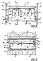
- FIGURE 3 is a side elevational segmented view illustrating an improved isolation passageway of the instant invention interposed between any two deposition chambers; and
- FIGURE 4 is a cross-sectional view taken along lines 4-4 shown in FIGURE 3.
- Referring now to the drawings and particularly to Figure 1, a photovoltaic cell 10 is shown formed from successive p-i-n layers, each of which is formed from a thin film semiconductor alloy material. The photovoltaic device such as a solar cell is made up of individual
p-i-n type cells - Each of the
cells conductivity semiconductor layer 16, anintrinsic semiconductor layer 18 and an n-type semiconductor layer 20. Although p-i-n photovoltaic cells are illustrated, the improved gas gate according to the present invention is equally adapted for use in multiple chamber apparatus which is adapted to produce tandem n-i-p cells by simply reversing the order depositing the n-type and p-type layers onto the substrate. Additionally, the disclosed deposition apparatus may be readily adapted to produce p-n cells, Schottky barrier cells as well as other semiconductor devices such as diodes, memory arrays, photoconductive devices and the like. It is to be understood that following the deposition of the semiconductor layers, a further deposition process may be either performed in a separate environment or as part of a continuous process. In further deposition processes, a "tco" (transparent conductive oxide)layer 22 preferably formed of indium tin oxide is added. Anelectrode grid 24 may be added to the device where the cell is of a sufficiently large area or if the conductivity of thetco layer 22 is insufficient. Thegrid 24 is adapted to shorten the carrier path and increase the conductive efficiency. - Referring now to Figure 2, a generally schematic representation of a multi-chambered glow discharge deposition processor 26 is illustrated r the continuous production of tandem or cascade-type photovoltaic cells. The apparatus 26 includes a plurality of isolated
dedicated deposition chambers isolation passageway 34 positioned between any two deposition chambers. Theexternal isolation passageway 34 is commonly referred to as a gas gate. - It should be apparent that, although one triad of deposition chambers is illustrated and described, additional triads or additional individual chambers may be added to the apparatus to provide the machine capability of producing tandem photovoltaic cells having p-i-n type configuration as illustrated in Figure 1, or n-i-p type, p-n type or n-p type configurations with a tco upper coating. However, for brevity of explanation, only two
gas gates 34 are shown between threerepresentative deposition chambers deposition chamber - Each of the
deposition chambers supply conduit 37 delivers process gas mixtures to the plasma regions created in eachdeposition chamber radio frequency generator 39. Although not shown, it should be apparent that exhaust conduits are also associated with each deposition chamber for withdrawing non-used gases and non-deposited plasma. - To form the photovoltaic cell 10 illustrated in Figure 1, a p-type amorphous
silicon alloy layer 16 is deposited onto the substrate 11 indeposition chamber 28, an intrinsic amorphoussilicon alloy layer 18 is deposited on the p-type layer 16 in thedeposition chamber 30 and an n-type amorphoussilicon alloy layer 20 is deposited atop theintrinsic layer 18 indeposition chamber 32. As a result, the apparatus 26 deposits at least three amorphous silicon alloy layers onto the substrate wherein the intrinsic layer deposited indeposition chamber 30 differs in composition from the layers deposited indeposition chambers - It is important that each of the alloy layers and particularly the intrinsic layer deposit onto a surface of the substrate 11 be of high purity in order to produce high efficiency photovoltaic devices 10. It is therefore necessary to substantially prevent the back diffusion of dopant process gases from either
chambers intrinsic deposition chamber 30. - Referring now to Figure 3, a
gas gate apparatus 34 is interposed betweendeposition chamber 28 anddeposition chamber 30 and betweendeposition chamber 30 anddeposition chamber 32. Eachgas gate 34 is identical and hence reference will only be made to the first gas gate betweenchambers gas gate 34 generally comprises alower block 44 and anupper block 46 with anisolation passageway 42 formed therebetween. Both the lower block and the upper block include a plurality ofapertures 47 inend panels gas gate 34 to the bulkhead between adjacent deposition chambers. The top surface of thelower block 44 formslower wall 53 ofisolation passageway 42 formed between the two deposition chambers. The lower surface of theupper block 46 forms theupper wall 55 ofisolation passageway 42. - In general, the
isolation passageway 42 is a relatively elongated narrow passageway that is sized to slidably receive substrate material 11 for passing therethrough fromdeposition chamber 28 todeposition chamber 30. Theopposed side walls 57 are therefore spaced greater than the width of substrate material 11. Thepassageway 42 has anentrance 43 and exit 45 for allowing the substrate material 11 to enter fromchamber 28 and exit tochamber 30. Theentrance 43 and exit 45 can have a height between 0.159 cm (1/16") and 1.27 cm (1/2") and a width of 29.2 cm (11 1/2").Guide rollers wall 55, across the gas gate from wall 72 to wall 73 and down along wall 73 toward exit 45. - The height of
passageway 42 is great enough to mount a plurality ofelectrodes 60 and groundedshields 62 therein vertically positioned aboveentrance 43 and exit 45. As shown in Figure 4, eachelectrode 60 extends substantially the whole width ofpassageway 42. As shown in Figure 3, twoelectrodes 60 are spaced along the length of thepassageway 42. Each electrode is made from a 0.635 cm (1/4") diameter stainless steel tube. The grounded shields 62 are made from stainless steel sheets bent in a substantially invented U-shape in cross section with twoside walls 64 and a spanning portion or spanningmiddle wall 66. Eachwall side wall 64 andmiddle portion 66 form aninterior space 68 defined within the concavity formed by the U-shaped shield with anopening 69. Theelectrodes 60 are positioned within theinterior space 68. Twoshields 62 are spacedly positioned along the length of thepassageway 42 such that there is agap 70 defined between twoadjacent side walls 64. The gap can be in approximately 15.24 cm (6" long). The inner end walls 72 and 73 ofupper block 46 are spaced from thenearest shield wall 64 by a gap of approximately 1.27 cm (1/2"). The spanningwall 66 is positioned to be interposed between theelectrodes 60 and the substrate 11. Each spanningwall 66 is spaced approximately from the substrate 11 between 1.27 cm (1/2") and 2.54 cm (1"). The substrate 11 is interposed betweenwalls 66 andwall 55. Theopening 69 to theinterior space 68 is opposite the spanningwall 66 and faces away from thewall 55 and the portion of the substrate 11adjacent wall 55. Theopening 69 is spaced fromlower wall 53 by approximately a one inch gap. - The electrodes are preferably connected to a low frequency alternating current such for example 75 Khz at 200 peak voltage. This electric field formed between the grounded
shield 62 and theelectrodes 60 are strong enough to ionize or molecularly fragment the process gaseous molecules that escape the deposition chambers through eitherentrance 43 or exit 45 into theisolation passageway 42 to form a plasma with theinterior space 68. After the plasma is formed, it is deposited or plated onto the interior surfaces 65 and 67 ofwalls shield 62. Theshields 62 contain the plasma and spatially isolates it from the remaining space of the gas gate. Theshields 62 prevent the plasma from depositing onto the substrate 11 which is also grounded. Other frequencies and voltages can be used with the general parameters that the voltage must be less than would cause sparking between the electrode and grounded shield and the frequency should be low enough to prevent the plasma from being over energized which would prevent it from landing on the shield. One can foresee using up to 1,000 volts before sparking and other problems due to extremely high voltage occur. - The total length of the
typical gate 34 can be under 30.5 cm (12 inches) long, with approximately two electrodes and shields spacedly positioned along the length of thepassageway 42. The serpentine path of the substrate 11 particularly aboutrollers 80 provide for a line of sight of any gaseous particles entering eitherentrance 43 or exit 45 to theplasma cavity 68. The grounding of the plasma onshield 62 provides for a chemical pump that also provides for attraction of gaseous molecules in the gas gate. - In this geometric fashion, it is a virtual 100% probability that a gaseous molecule or processing gas from the
deposition chambers 28 will migrate into one of theinterior spaces 68 during its back diffusion migration fromchamber 28 towardchamber 30. As such thechamber 30 is effectively isolated fromchamber 28 and any possible contamination fromchamber 28 is eliminated by the active destruction of free gaseous molecules escaping fromchamber 28 by the electrodes and shields 62 within theisolation passageway 42. - In this fashion, a
gas gate 34 withisolation passageway 42 can effectively isolate a series of deposition chambers from each other. Thegas gate 34 is compatible to use sweep gases in addition if so desired. However thegas gate 34 by actively eliminating gaseous molecules is not solely dependent on molecular collisions to prevent back diffusion of gaseous molecules from thedeposition chamber 28 toward theintrinsic deposition chamber 30. As such, thegas gate 34 can be relatively shorter than comparable flow gas gates used at extremely low pressures in the area of 0.133 Pa (1 millitorr) in a continuous deposition process for forming photovoltaic cells. - The
plasma generating region 68 may also be magnetically enhanced bypermanent magnets 84 attached to theside walls 57. Themagnets 84 provide curvature to the path of any plasma particle thereby increasing its path distance and probability of colliding with a gaseous particle causing an avalanche of plasma generating particles each also curving as it moves in the magnetic field. - An
optional vacuum pump 86 can also be attached to thegas gate 34 to evacuate thegas gate 34 of gaseous particles. Furthermore, the gas gate can include the use of sweep gases as is known in the art. - It is also foreseen that the electrodes can be replaced with a microwave generating antenna that directs electromagnetic radiation into
region 68 to provide a plasma generating mechanism.
Claims (15)
- An isolation passageway (34) adapted to operatively interconnect first and second adjacent low pressure deposition chambers (28, 30) wherein a first semiconductor layer (16) is deposited on a substrate (11) in said first chamber (28) and a second semiconductor layer (18) is deposited on said substrate (11) in said second chamber (30), to provide reduced diffusion of process gases between said first and second chambers (28, 30), and to provide passage of said substrate (11) therethrough; said passageway characterized by:a plasma generating means (60) for converting said process gases in said isolation passageway (34) into a plasma; andan attraction means (62) for electrically attracting said plasma and spatially isolating said plasma away from said substrate.
- An isolation passageway as defined in claim 1 further characterized by:
a plurality of plasma generating means (60) spacedly positioned along the length of said passageway (34), each of said generating plasma means (60) being elongated and extending transversely across said passageway (34). - An isolation passageway as defined in claim 2 further characterized by:
said attraction means (62) being interposed between said plasma generating means (60) and said substrate (11). - An isolation passageway as defined in claim 1 further characterized by:
a grounded shield (62) for partially defining a space for said spatially isolated plasma and for grounding said plasma thereon. - An isolation passageway as defined in claim 1 further characterized by:a plurality of plasma producing electrodes (60) positioned in said passageway for producing a plasma from any process gases in said isolation passageway; anda plurality of grounded electrode shields (62) positioned in said passageway and constructed and positioned to be plated by said plasma to prevent plasma within said isolation passageway from depositing on said substrate (11).
- An isolation passageway as defined in claim 5 further characterized by:said shields (62) each having a substantially U-shaped cross section and elongated to co-extend substantially with said electrode (60); andeach said electrode (60) being positioned within the interior space defined by a respective U-shaped shield (62).
- An isolation passageway as defined in claim 6 further characterized by:said electrodes (60) and shields (62) each extending transversely across said passageway (34); andsaid electrodes (60) and shields (62) being spacedly positioned along the length of said passageway (34).
- An isolation passageway as defined in claim 6 further characterized by:
said shields (62) having a midportion (66) interposed between said electrodes (60) and said substrate (11). - An isolation passageway as defined in claim 8 further characterised by:said shields (62) having a downwardly facing opening (69); andsaid passageway (34) defining a path for the substrate (11) such that said substrate (11) enters said passageway (34) at a point (43) below said openings of said shields (69) and passes upwardly above and over said shields (62) and downwardly to a point (45) below said shields (62) where it exits said passageway (34).
- An isolation passageway as defined in claim 6 further characterized by:said electrodes (60) and shields (62) each extending transversely across said passageway (34); andsaid electrodes (60) and shields (62) being spacedly positioned along the length of said passageway (34).
- An isolation passageway as defined in claim 5 further characterized by:
said shields (62) being interposed between said electrodes (60) and said substrate (11). - An isolation passageway as defined in claim 11 further characterized by:said shields (62) having a downwardly facing opening (69); andsaid passageway (34) defining a path for the substrate (11) such that said substrate (11) enters said passageway (34) at a point (43) below said openings of said shields (69) and passes upwardly above and over said shields (62) and downwardly to a point (45) below said shields (62) where it exits said passageway (34).
- An isolation passageway as defined in claim 5 further characterized by:
said electrodes (60) being connected to a low frequency alternating current potential. - An isolation passageway as defined in claim 5 further characterized by:
said shields (62) each being contoured substantially about a perimeter of an electrode (60) and defining a cavity (68) in which said electrode (60) is positioned and said shield (62) having an opening (69) facing away from a portion of said substrate (11). - An isolation passageway as defined in claim 14 further characterized by:said shields (62) having a downwardly facing opening (69); andsaid passageway (34) defining a path for the substrate (11) such that said substrate (11) enters said passageway at a point (43) below said openings of said shields (69) and passes upwardly above and over said shields (62) and downwardly to a point below (45) said shields (62) where it exits said passageway.
Applications Claiming Priority (3)
| Application Number | Priority Date | Filing Date | Title |
|---|---|---|---|
| US723042 | 1991-06-28 | ||
| US07/723,042 US5090356A (en) | 1991-06-28 | 1991-06-28 | Chemically active isolation passageway for deposition chambers |
| PCT/US1992/005158 WO1993000455A1 (en) | 1991-06-28 | 1992-06-18 | Chemically active isolation passageway for deposition chambers |
Publications (3)
| Publication Number | Publication Date |
|---|---|
| EP0591398A1 EP0591398A1 (en) | 1994-04-13 |
| EP0591398A4 EP0591398A4 (en) | 1995-01-11 |
| EP0591398B1 true EP0591398B1 (en) | 1997-10-15 |
Family
ID=24904572
Family Applications (1)
| Application Number | Title | Priority Date | Filing Date |
|---|---|---|---|
| EP92914370A Expired - Lifetime EP0591398B1 (en) | 1991-06-28 | 1992-06-18 | Chemically active isolation passageway for deposition chambers |
Country Status (5)
| Country | Link |
|---|---|
| US (1) | US5090356A (en) |
| EP (1) | EP0591398B1 (en) |
| AU (1) | AU2260892A (en) |
| DE (1) | DE69222768D1 (en) |
| WO (1) | WO1993000455A1 (en) |
Families Citing this family (10)
| Publication number | Priority date | Publication date | Assignee | Title |
|---|---|---|---|---|
| US5411592A (en) * | 1994-06-06 | 1995-05-02 | Ovonic Battery Company, Inc. | Apparatus for deposition of thin-film, solid state batteries |
| JP3428865B2 (en) | 1997-07-09 | 2003-07-22 | キヤノン株式会社 | Apparatus and method for forming deposited film |
| JPH11246971A (en) * | 1998-03-03 | 1999-09-14 | Canon Inc | Method and apparatus for producing microcrystalline silicon-based thin film |
| JP3349953B2 (en) * | 1998-05-25 | 2002-11-25 | シャープ株式会社 | Substrate processing equipment |
| US6041817A (en) * | 1998-08-21 | 2000-03-28 | Fairchild Semiconductor Corp. | Processing system having vacuum manifold isolation |
| WO2006053128A2 (en) * | 2004-11-10 | 2006-05-18 | Daystar Technologies, Inc. | Pallet based system for forming thin-film solar cells |
| WO2006053218A2 (en) * | 2004-11-10 | 2006-05-18 | Daystar Technologies, Inc. | Pressure control system in a photovoltaic substrate deposition |
| US7176543B2 (en) * | 2005-01-26 | 2007-02-13 | United Solar Ovonic Corp. | Method of eliminating curl for devices on thin flexible substrates, and devices made thereby |
| KR102021845B1 (en) * | 2011-04-28 | 2019-09-18 | 가부시키가이샤 가네카 | Flexible printed circuit integrated with reinforcing plate |
| US9435028B2 (en) * | 2013-05-06 | 2016-09-06 | Lotus Applied Technology, Llc | Plasma generation for thin film deposition on flexible substrates |
Family Cites Families (4)
| Publication number | Priority date | Publication date | Assignee | Title |
|---|---|---|---|---|
| US4626447A (en) * | 1985-03-18 | 1986-12-02 | Energy Conversion Devices, Inc. | Plasma confining apparatus |
| US4664951A (en) * | 1985-07-31 | 1987-05-12 | Energy Conversion Devices, Inc. | Method provided for corrective lateral displacement of a longitudinally moving web held in a planar configuration |
| US4723507A (en) * | 1986-01-16 | 1988-02-09 | Energy Conversion Devices, Inc. | Isolation passageway including annular region |
| US4920917A (en) * | 1987-03-18 | 1990-05-01 | Teijin Limited | Reactor for depositing a layer on a moving substrate |
-
1991
- 1991-06-28 US US07/723,042 patent/US5090356A/en not_active Expired - Lifetime
-
1992
- 1992-06-18 DE DE69222768T patent/DE69222768D1/en not_active Expired - Lifetime
- 1992-06-18 AU AU22608/92A patent/AU2260892A/en not_active Abandoned
- 1992-06-18 WO PCT/US1992/005158 patent/WO1993000455A1/en not_active Ceased
- 1992-06-18 EP EP92914370A patent/EP0591398B1/en not_active Expired - Lifetime
Also Published As
| Publication number | Publication date |
|---|---|
| US5090356A (en) | 1992-02-25 |
| WO1993000455A1 (en) | 1993-01-07 |
| AU2260892A (en) | 1993-01-25 |
| EP0591398A4 (en) | 1995-01-11 |
| DE69222768D1 (en) | 1997-11-20 |
| EP0591398A1 (en) | 1994-04-13 |
Similar Documents
| Publication | Publication Date | Title |
|---|---|---|
| US4438724A (en) | Grooved gas gate | |
| US4132613A (en) | Glow discharge method and apparatus | |
| US4537795A (en) | Method for introducing sweep gases into a glow discharge deposition apparatus | |
| US4480585A (en) | External isolation module | |
| US5090356A (en) | Chemically active isolation passageway for deposition chambers | |
| US4450786A (en) | Grooved gas gate | |
| US4479455A (en) | Process gas introduction and channeling system to produce a profiled semiconductor layer | |
| US4462333A (en) | Process gas introduction, confinement and evacuation system for glow discharge deposition apparatus | |
| US4520757A (en) | Process gas introduction, confinement and evacuation system for glow discharge deposition apparatus | |
| US4513684A (en) | Upstream cathode assembly | |
| EP0109148B1 (en) | Substrate shield for preventing the deposition of nonhomogeneous films | |
| US4608943A (en) | Cathode assembly with localized profiling capabilities | |
| EP0118643B1 (en) | Cathode assembly for glow discharge deposition apparatus | |
| US4626447A (en) | Plasma confining apparatus | |
| KR100254120B1 (en) | Method of Forming Semiconductor Thin Film | |
| EP0100611B1 (en) | Reduced capacitance electrode assembly | |
| EP4331003B1 (en) | Method and devices for plasma treatment | |
| EP0106521B1 (en) | Baffle system for glow discharge deposition apparatus | |
| DE19919742A1 (en) | Doped silicon substrates are coated with an anti-reflection layer, especially of silicon nitride for solar cells, by sputter deposition using silicon electrodes alternately connected as cathode and anode | |
| JP2000096224A (en) | Magnetron sputtering apparatus and film forming method using the apparatus | |
| CN121862670A (en) | Constraint ring, plasma processing apparatus and method | |
| JPS59136476A (en) | Apparatus for plasma vapor-phase reaction | |
| JP2001118699A (en) | Plasma treatment apparatus and method of plasma treatment |
Legal Events
| Date | Code | Title | Description |
|---|---|---|---|
| PUAI | Public reference made under article 153(3) epc to a published international application that has entered the european phase |
Free format text: ORIGINAL CODE: 0009012 |
|
| AK | Designated contracting states |
Kind code of ref document: A1 Designated state(s): DE ES FR GB IT |
|
| 17P | Request for examination filed |
Effective date: 19931224 |
|
| A4 | Supplementary search report drawn up and despatched |
Effective date: 19941118 |
|
| AK | Designated contracting states |
Kind code of ref document: A4 Designated state(s): DE ES FR GB IT |
|
| 17Q | First examination report despatched |
Effective date: 19960208 |
|
| GRAG | Despatch of communication of intention to grant |
Free format text: ORIGINAL CODE: EPIDOS AGRA |
|
| GRAH | Despatch of communication of intention to grant a patent |
Free format text: ORIGINAL CODE: EPIDOS IGRA |
|
| GRAH | Despatch of communication of intention to grant a patent |
Free format text: ORIGINAL CODE: EPIDOS IGRA |
|
| GRAA | (expected) grant |
Free format text: ORIGINAL CODE: 0009210 |
|
| AK | Designated contracting states |
Kind code of ref document: B1 Designated state(s): DE ES FR GB IT |
|
| PG25 | Lapsed in a contracting state [announced via postgrant information from national office to epo] |
Ref country code: IT Free format text: LAPSE BECAUSE OF FAILURE TO SUBMIT A TRANSLATION OF THE DESCRIPTION OR TO PAY THE FEE WITHIN THE PRESCRIBED TIME-LIMIT;WARNING: LAPSES OF ITALIAN PATENTS WITH EFFECTIVE DATE BEFORE 2007 MAY HAVE OCCURRED AT ANY TIME BEFORE 2007. THE CORRECT EFFECTIVE DATE MAY BE DIFFERENT FROM THE ONE RECORDED. Effective date: 19971015 Ref country code: FR Free format text: LAPSE BECAUSE OF FAILURE TO SUBMIT A TRANSLATION OF THE DESCRIPTION OR TO PAY THE FEE WITHIN THE PRESCRIBED TIME-LIMIT Effective date: 19971015 Ref country code: ES Free format text: THE PATENT HAS BEEN ANNULLED BY A DECISION OF A NATIONAL AUTHORITY Effective date: 19971015 |
|
| REF | Corresponds to: |
Ref document number: 69222768 Country of ref document: DE Date of ref document: 19971120 |
|
| PG25 | Lapsed in a contracting state [announced via postgrant information from national office to epo] |
Ref country code: DE Free format text: LAPSE BECAUSE OF FAILURE TO SUBMIT A TRANSLATION OF THE DESCRIPTION OR TO PAY THE FEE WITHIN THE PRESCRIBED TIME-LIMIT Effective date: 19980116 |
|
| EN | Fr: translation not filed | ||
| PLBE | No opposition filed within time limit |
Free format text: ORIGINAL CODE: 0009261 |
|
| STAA | Information on the status of an ep patent application or granted ep patent |
Free format text: STATUS: NO OPPOSITION FILED WITHIN TIME LIMIT |
|
| 26N | No opposition filed | ||
| REG | Reference to a national code |
Ref country code: GB Ref legal event code: IF02 |
|
| PGFP | Annual fee paid to national office [announced via postgrant information from national office to epo] |
Ref country code: GB Payment date: 20110628 Year of fee payment: 20 |
|
| REG | Reference to a national code |
Ref country code: GB Ref legal event code: PE20 Expiry date: 20120617 |
|
| PG25 | Lapsed in a contracting state [announced via postgrant information from national office to epo] |
Ref country code: GB Free format text: LAPSE BECAUSE OF EXPIRATION OF PROTECTION Effective date: 20120617 |