EP0590304B1 - Method for the pilot control of a switched power supply for the compensation of variations of the distribution voltage - Google Patents
Method for the pilot control of a switched power supply for the compensation of variations of the distribution voltage Download PDFInfo
- Publication number
- EP0590304B1 EP0590304B1 EP93113561A EP93113561A EP0590304B1 EP 0590304 B1 EP0590304 B1 EP 0590304B1 EP 93113561 A EP93113561 A EP 93113561A EP 93113561 A EP93113561 A EP 93113561A EP 0590304 B1 EP0590304 B1 EP 0590304B1
- Authority
- EP
- European Patent Office
- Prior art keywords
- voltage
- circuit
- power supply
- switched
- control signal
- Prior art date
- Legal status (The legal status is an assumption and is not a legal conclusion. Google has not performed a legal analysis and makes no representation as to the accuracy of the status listed.)
- Expired - Lifetime
Links
Images


Classifications
-
- H—ELECTRICITY
- H02—GENERATION; CONVERSION OR DISTRIBUTION OF ELECTRIC POWER
- H02M—APPARATUS FOR CONVERSION BETWEEN AC AND AC, BETWEEN AC AND DC, OR BETWEEN DC AND DC, AND FOR USE WITH MAINS OR SIMILAR POWER SUPPLY SYSTEMS; CONVERSION OF DC OR AC INPUT POWER INTO SURGE OUTPUT POWER; CONTROL OR REGULATION THEREOF
- H02M3/00—Conversion of dc power input into dc power output
- H02M3/02—Conversion of dc power input into dc power output without intermediate conversion into ac
- H02M3/04—Conversion of dc power input into dc power output without intermediate conversion into ac by static converters
- H02M3/10—Conversion of dc power input into dc power output without intermediate conversion into ac by static converters using discharge tubes with control electrode or semiconductor devices with control electrode
- H02M3/145—Conversion of dc power input into dc power output without intermediate conversion into ac by static converters using discharge tubes with control electrode or semiconductor devices with control electrode using devices of a triode or transistor type requiring continuous application of a control signal
- H02M3/155—Conversion of dc power input into dc power output without intermediate conversion into ac by static converters using discharge tubes with control electrode or semiconductor devices with control electrode using devices of a triode or transistor type requiring continuous application of a control signal using semiconductor devices only
- H02M3/156—Conversion of dc power input into dc power output without intermediate conversion into ac by static converters using discharge tubes with control electrode or semiconductor devices with control electrode using devices of a triode or transistor type requiring continuous application of a control signal using semiconductor devices only with automatic control of output voltage or current, e.g. switching regulators
-
- G—PHYSICS
- G05—CONTROLLING; REGULATING
- G05F—SYSTEMS FOR REGULATING ELECTRIC OR MAGNETIC VARIABLES
- G05F1/00—Automatic systems in which deviations of an electric quantity from one or more predetermined values are detected at the output of the system and fed back to a device within the system to restore the detected quantity to its predetermined value or values, i.e. retroactive systems
- G05F1/10—Regulating voltage or current
- G05F1/46—Regulating voltage or current wherein the variable actually regulated by the final control device is dc
- G05F1/56—Regulating voltage or current wherein the variable actually regulated by the final control device is dc using semiconductor devices in series with the load as final control devices
- G05F1/563—Regulating voltage or current wherein the variable actually regulated by the final control device is dc using semiconductor devices in series with the load as final control devices including two stages of regulation at least one of which is output level responsive, e.g. coarse and fine regulation
-
- H—ELECTRICITY
- H02—GENERATION; CONVERSION OR DISTRIBUTION OF ELECTRIC POWER
- H02M—APPARATUS FOR CONVERSION BETWEEN AC AND AC, BETWEEN AC AND DC, OR BETWEEN DC AND DC, AND FOR USE WITH MAINS OR SIMILAR POWER SUPPLY SYSTEMS; CONVERSION OF DC OR AC INPUT POWER INTO SURGE OUTPUT POWER; CONTROL OR REGULATION THEREOF
- H02M1/00—Details of apparatus for conversion
- H02M1/0003—Details of control, feedback or regulation circuits
- H02M1/0016—Control circuits providing compensation of output voltage deviations using feedforward of disturbance parameters
- H02M1/0022—Control circuits providing compensation of output voltage deviations using feedforward of disturbance parameters the disturbance parameters being input voltage fluctuations
Definitions
- the invention relates to a method for pilot control of a Switching power supply to compensate for fluctuations in the Supply voltage according to the preamble of patent claim 1 and a circuit arrangement for performing the method according to the preamble of claim 3.
- the integrated circuits described include a frequency generator, a ramp generator, a comparator, the output signal of the ramp generator with a depending on Current value of the output voltage of the switching power supply (and thus the voltage level determined by the load current) and a flip-flop from the frequency generator and is controlled by said comparator and thus for normal operation the pulse duration of the control pulses for the one or more electronic switches with the control circuit realized switching power supply.
- the slope of the rising edge of the output signal of the ramp generator is by varying a control current changeable.
- This known method for pilot control in which the Ramp slope is controlled, makes sense for supply voltages, that do not deviate too much from a nominal value, for example for rectified sinusoidal voltages, which are partially smoothed out by a capacitance. Because the slope of the rising edge of a ramp generator output cannot be changed arbitrarily, in particular, can not be of any size, as is the case with large deviations of the supply voltages from a medium one Upward value would be required is known Switch-mode power supplies either a preparation of the supply voltage, for example with the help of a capacity, or an adjustment of fluctuations in the supply voltage the controller that keeps the output voltage constant is required.
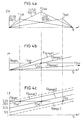
- Figure 4a shows a schematic representation of the current through the choke of a step-up converter for the exemplary case that the DC output voltage UA is 300 V and a sinusoidal input voltage UI with a peak value ⁇ I of 300 V is provided as the supply voltage.
- the instantaneous value of the input voltage UI is provided as a parameter and FIG. 4a shows the target duty cycle related to the respective input voltage for a certain constant load.
- the pulse duty factor n 2setpoint is obtained with a momentary value of the input voltage UI of 150 V
- FIG. 4b shows the voltage curve at two signal inputs of a comparator, which is responsible for the precontrol in the case of a precontrol by means of a variable ramp slope.
- the horizontal straight line labeled U controller represents the output voltage of a controller related to a specific, constant load.
- the ramp voltage U ramp2 is set at an input voltage UI of 150 V. The intersection of this ramp with the controller output voltage defines the duty cycle n 2actual .
- this ramp is not the controller output voltage U intersects regulator within the displayed period.
- the pre-control by means of controlled ramp slope works well only at input voltages which are close to the nominal value for which the pre-control was dimensioned.
- the object of the invention is to provide a method for pilot control of a switching power supply, with which large fluctuations in the supply voltage can be compensated can.
- a circuit arrangement for performing a method according to one of claims 1 or 2 is the subject of 3.
- a favorable embodiment of a such circuit arrangement is the subject of the claim 4th
- a method according to the invention for pilot control of a Switching power supply to compensate for fluctuations in the supply voltage differs from one described above State of the art method primarily by that a ramp voltage with a DC component and with a fixed ramp slope with one depending from the instantaneous value of the output voltage of the switching power supply specified voltage level is compared and that the pilot control by changing the DC component the ramp is made.
- This method according to the invention can be used implement error-free feedforward control, i.e. the feedforward control Fluctuations in the input voltage UI fully compensated and the voltage regulator is only load-related Must compensate for fluctuations.
- Figure 1 shows a possible embodiment of an inventive Circuit arrangement for performing a The method of claim 1 or 2, combined with one typical step-up regulator (step-up converter).
- step-up converter can be a circuit arrangement according to the invention also for controlling other switching power supply basic circuits are used, such as a step-down regulator (Buck converter), an inverter, an up-down regulator (Step-down converter), a flyback converter or one Flow converter in single-ended or push-pull circuit.
- FIG. 1 shows a rectifier arrangement G with two input terminals e1 and e2 and 2 output terminals x and y shown.
- the input terminals el and e2 are with an alternating voltage UO charged.
- the output terminals of the Rectifier circuit G, x and y accordingly set one unsmoothed, alternating DC voltage UI ready.
- Terminals x and y are also input terminals the step-up converter basic circuit is provided.
- This Booster has two output terminals z and y, on which an output DC voltage UA is provided.
- the control circuit of this step-up converter contains one Frequency generator FG, the frequency of which against a reference potential switched capacity CG and by one against Reference potential switched resistor RG set is.
- the output of the frequency generator FG is at one Clock input of a frequency ramp generator FRG and on an input of a logic circuit LS switched.
- a frequency ramp generator FRG has an input terminal rr, which with a from the instantaneous value of the input voltage UI the terminals x and y of the switching power supply dependent electrical Size is applied.
- the frequency ramp generator FRG provides a ramped output signal its frequency from the output frequency of the frequency generator FG depends and a DC component is superimposed on it is.
- the DC voltage component of the output signal of the frequency ramp generator FRG is dependent on an electrical variable provided at the terminal rr changed.
- the electrical quantity provided to rr is depending on the instantaneous value of the input voltage UI to the Terminals x and y of the switching power supply.
- a current is applied to the input terminal rr impressed by the fact that between the terminal x and the input terminal A resistor RR is provided.
- the output terminal z of the step-up converter is via a Voltage divider formed from a first divider resistor RT1 and a second divider resistor RT2 against Reference potential ground switched.
- the connection node between the two resistors RT1 and RT2, one for Output voltage UA provides proportional voltage, is connected to an input of a voltage regulator SR.
- the voltage regulator SR gives depending from the output voltage UA between the output terminals z and y of the step-up converter shown is a controller output signal from. This is the output of the voltage regulator SR with one input, here with a non-inverting one Input, a comparator circuit K1 connected.
- the output of said frequency ramp generator FRG is with another input, here an inverting input this comparator K1 interconnected.
- the exit this comparator circuit K1 has an input of said logic circuit LS connected.
- the logic circuit LS provides a control signal for activation at its output of the semiconductor switch HS ready, which depends on the Output quantity of the comparator circuit K1 and of the output signal of the frequency generator FG.
- the output signal the logic circuit LS is a pulse width modulated Signal whose repetition frequency is determined by the output frequency of the frequency generator FG is determined and its Pulse duration by the output of the comparator circuit K1 is set.
- the output signal of the comparator K1 is caused by a falling edge of the output signal of the frequency ramp generator put in a logical state and this logical state changes as soon as the instantaneous value the rising edge of the output signal of the Frequency ramp generator FRG from the voltage regulator SR provided reference voltage reached. Too big Pulse widths at the output of the logic circuit LS and thus too large on times of the semiconductor switch HS as a result of brief load-related control vibrations of the voltage regulator Avoiding SR can, as shown in Figure 1, the comparator K1 with another non-inverting Be equipped on a fixed entrance Basic voltage UTG is kept.
- the duty cycle of the frequency generator FG defines the Limit values for the ratio of the on-time of the semiconductor switch HS for the period of the control circuit firmly.
- Figure 2 shows the boost converter basic circuit of Figure 1 with a special frequency generator circuit FGS, with a special embodiment of the logic circuit LS as well as with an additional protective circuit PC that an overload of the switching power supply if the output voltage is too high UA or excessive current through the choke L prevented.
- Frequency generator FGS is a frequency generator which provides both a square wave signal and also a ramp signal.
- the ramp-shaped output signal this frequency generator FGS is a DC voltage superimposed, the value of one in an input terminal rr of the frequency generator FGS fed electrical Size depends.
- the frequency generator FGS has a control current input terminal rr that with the control current input a5 an input current mirror circuit CM5 is interconnected.
- a current mirror circuit is a current mirror basic circuit consisting of two bipolar transistors Ta5 and Rb5 shown, their common Base connection with the collector connection of the transistor Ta5 is interconnected and the control current input a5 forms and their emitter connections together to a reference potential are switched.
- the collector connection of the Transistor Tb5 is connected to current output b5.
- This current mirror circuit CM5 is used in the embodiment shown as a current sink. Of the Current output b5 of the current mirror circuit CM5 is with the Control current input a4 of another current mirror circuit CM4 interconnected.
- This current mirror circuit CM4 is designed as a current source in the embodiment in an analogous manner to the current mirror circuit CM5 two pnp transistors Tb4 and Ta4 is formed.
- the collector connection of the transistor Tb4 is in this case the current output of the current mirror circuit CM4 interconnected.
- the emitter connections of the two transistors Ta4 and Tb4 are connected to a supply potential VCC.
- the current output b4 of the current source CM5 forms the Output of the input stage ES and is with an internal Control current input rri connected.
- the input stage ES for the control current is used to control the control current input rr to decouple the following circuit.
- the control current input rri forms a current node with one against that Supply potential VCC switched current source I2, the Current output of a current mirror circuit designed as a current sink CM1, the base terminal of a transistor T2 and a terminal of a resistor R2, the other Connection with the opposite of the supply potential VCC Potential mass is applied.
- the exemplary embodiment is the current mirror circuit CM1 in analogous to the current mirror circuit CM5 built with an output transistor Tb1, the collector terminal of which Current output bl forms and with an input transistor Ta1, its collector connection together with the base connection of transistor Ta1 and transistor Tb1 Control current input al forms.
- the transistor T2 is shown in the Embodiment as a multi-collector transistor executed and a collector of this transistor T2 is with connected to the control current input al of the current source CM1.
- the transistor T2 is in the exemplary embodiment as a pnp transistor formed, whose emitter connection with the emitter connection another pnp transistor T1 connected together is and together with this with the current output a current source IO is connected, which is against the supply potential VCC is switched.
- the base connection of the also designed as a multi-collector transistor T1 is at reference potential via a capacitance CG Ground switched.
- the switched as a power source Current mirror CM3 is analogous to that Current mirror CM4 formed from two pnp transistors Ta3 and Tb3, the collector terminal of transistor Tb3 represents the current output of the circuit CM3 and the collector connection of the transistor Ta3 with the control current input a3 is connected.
- the control current input of the current mirror CM3 is at reference potential via a resistor RG Ground switched.
- the resistance RG essentially sets together with the capacitance CG, the frequency of the frequency generator firmly.
- the control current input a2 of the current mirror circuit CM2, which consists of two npn transistors Ta2 and Tb2 implemented analogously to the current mirror circuit CM5 is via a current source I1 with the supply potential VCC connected.
- the collector connection of an NPN transistor T3 is the control current input a2 Current mirror circuit CM2 interconnected and the emitter connection this transistor T3 is against reference potential Ground switched and thus with the emitter connections of the transistors Ta2 and Tb2 connected.
- the basic connection this transistor T3 is connected to a collector terminal of the Transistor T1 interconnected and through a resistor R1 connected to ground reference potential.
- the two Transistors T1 and T2 are operated as an oscillator circuit, wherein the transistor T2 switches the switching thresholds and transistor T1 between charging and Discharge of the capacity CG switches. Because of this constellation any small frequencies can be switched.
- the Current mirror circuit CM1 in a collector circuit of the Transistor T2 leads to positive feedback, so that the Circuit can switch abruptly.
- the push-pull transistors T1 and T2 must be controlled from saturation become, which leads to a loss of time. Because of the low, required to switch a decoupling stage Voltage hub and because there are no capacities within the push-pull stage must be reloaded, however the overall arrangement, consisting of the oscillator stage and a decoupling stage AK quickly.
- the second collector connection of the transistor T1 is connected to a terminal a Coupling stage AK connected.
- the second collector connection of the transistor T2 is at a terminal b of the decoupling stage AK switched and also to the base connection of an in this decoupling stage contained transistor T4.
- the clamp is b as a current output terminal of a current mirror circuit intended.
- This current mirror circuit is a current sink is formed and is made up of two transistors Ta and Tb in known manner formed.
- the collector connection of transistor Tb connected to terminal b and the base connection of the transistors Ta and Tb is common with the collector terminal of the transistor Ta with the Current input terminal a of this current mirror circuit and thus the decoupling stage AK connected.
- the emitter connections of the two transistors Ta and Tb are at reference potential Ground switched.
- the emitter connection of the as coupling transistor provided transistor T4 is also on Reference potential ground switched.
- the collector connection of the transistor T4 is a so-called open collector the signal output terminal OFG of the frequency generator FGS connected.
- the resistor R3 between the base connection the coupling transistor T4 and the current output b the current sink from the transistors Ta and Tb becomes the switchover time this decoupling stage is shortened.
- the transistors Ta and Tb are operated in saturation.
- the resistance R3 reduces the stroke of the decoupling stage because it reduces the Voltage at the base of the coupling transistor T4 to approx. Holds 0.4 V.
- the arrangement according to Figure 3 is at the output terminal OFG an oscillator signal ready and at the output terminal OFRG, due to the integrating effect of the capacity CG is a ramp signal with the same frequency.
- the base voltage on Transistor T1 is the same size as the base voltage on Transistor T2, this leads to a low collector current in transistor T2 and the current mirror circuit CM1, the is connected as a current sink, leads from the base connection of the Transistor T2 a current from the current output b1. Because of the positive feedback, this current grows very quickly on, so that the transistor T1 no longer has a collector current leads. The base voltage at transistor T2 is set to lower threshold pulled. If the transistor T1 does not Collector current, none falls across resistor R1 Tension off. Because of this, it discharges as a current sink switched current mirror circuit CM2 via the current output b2 and the diode D1 the capacitance CG.
- the current mirror circuit CM2 is used to unload the capacity CG and the current mirror circuit CM3 is used for charging the capacity CG.
- the ratio of rising to falling Flank one at the capacitance CG and thus at the Output terminal DFRG applied signals can by the Current ratio of the current sink CM2 and the current source CM3 can be set.
- FIG. 4c shows the voltage curve at two signal inputs of a comparator, which is responsible for the pilot control in the case of a pilot control according to the invention.
- Figure 4c thus shows a similar context as Figure 4b, but with the difference that the ramp voltage U RAMPE1 do not differ from the ramp voltage U RAMPE2 and from the ramp voltage U RAMPE3 in their pitch but by the height of the ramp superimposed DC voltage.
- the ramps U RAMPE1 , U RAMPE2 and U RAMPE3 thus run parallel to one another. In the example shown in FIG.
- the point of intersection of the respective ramp voltage with the reference voltage U REGLER lies on the comparator in such a way that the actual duty cycles n 1act , n 2act and n 3act respectively the target duty ratios n 1SOLL , n 2SOLL and n 3SOLL for an optimal one Precontrol, as shown in Figure 4a, correspond.
- feedforward control is used not on the embodiment of the embodiment limited.
- the same procedure can also be used Flyback converter switching power supplies, with step-up / step-down converters and can be used with buck converters.
Description
Die Erfindung betrifft ein Verfahren zur Vorsteuerung eines
Schaltnetzteiles zum Ausgleich von Schwankungen der
Speisespannung nach dem Oberbegriff des Patentanspruchs 1
sowie eine Schaltungsanordnung zur Durchführung des Verfahrens
nach dem Oberbegriff des Patentanspruchs 3.The invention relates to a method for pilot control of a
Switching power supply to compensate for fluctuations in the
Supply voltage according to the preamble of
Sowohl Eintakt- als auch Gegentaktschaltnetzteile, insbesondere
mit integrierten Steuerschaltungen, bei denen zum
Ausgleich von Schwankungen der Speisespannung eine Vorsteuerung
vorgesehen ist, sind bekannt. Unter anderem in
dem Datenbuch 1989/90 "ICS für Industrielle Anwendungen"
der Fa. Siemens AG, Seiten 182 bis 231 und 242 bis 260
sind komerziell erhältliche integrierte Steuerschaltungen
TDA4700, TDA4718, TDA4716, TDA4714, TDA4918 und TDA4919
sowie deren Anwendung in Schaltnetzteilen beschrieben.
Auch in dem Nachdruck von Siemens Components 5/88, S. 191
bis 194, 6/88, S. 260 bis 265 und 1/89, S. 12 bis 17 von
R. Blöckl, erschienen unter dem Titel "TDA 4918/4919 - New
Generation of Control ICs for Switched-Mode Power
Supplies" insbesondere in Figur 3 des Teil 2, sind solche
Schaltnetzteile gezeigt. Bei allen diesen Steuerschaltkreisen
wird zum Ansteuern der elektronischen Schalter von
mit diesen aufgebauten Schaltnetzteilen ein pulsdauermoduliertes
Signal bereitgestellt, wobei die Pulsdauer sowohl
von einer Ausgangsspannungsreglerschaltung als auch von
einer die Speisespannung berücksichtigenden Vorsteuerung
festgelegt wird. Die beschriebenen integrierten Schaltkreise
enthalten unter anderem einen Frequenzgenerator,
einen Rampengenerator, einen Komparator, der das Ausgangssignal
des Rampengenerators mit einem in Abhängigkeit vom
Momentanwert der Ausgangsspannung des Schaltnetzteiles
(und somit vom Laststrom) festgelegten Spannungspegel vergleicht
und ein Flip-Flop, das vom Frequenzgenerator und
von dem besagten Komparator angesteuert wird und somit für
den Normalbetrieb die Impulsdauer der Ansteuerimpulse für
den bzw. die elektronischen Schalter eines mit der Ansteuerschaltung
realisierten Schaltnetzteiles festlegt.
Die Steigung der steigenden Flanke des Ausgangssignales
des Rampengenerators ist durch Variation eines Steuerstromes
veränderbar.Both single-ended and push-pull switching power supplies, in particular
with integrated control circuits, in which
Compensation of fluctuations in the supply voltage a pilot control
are provided are known. Among other things in
the data book 1989/90 "ICS for industrial applications"
from Siemens AG, pages 182 to 231 and 242 to 260
are commercially available integrated control circuits
TDA4700, TDA4718, TDA4716, TDA4714, TDA4918 and TDA4919
as well as their application in switching power supplies.
Also in the reprint from Siemens Components 5/88, p. 191
to 194, 6/88, pp. 260 to 265 and 1/89, pp. 12 to 17 from
R. Blöckl, published under the title "TDA 4918/4919 - New
Generation of Control ICs for Switched-Mode Power
Supplies ", in particular in FIG. 3 of
Bei den bekannten Schaltnetzteilen wird ein Verfahren zur Vorsteuerung eingesetzt, die dem Ausgleich von Speisespannungsschwankungen dient, wobei eine Veränderung der Speisespannung zu einer Veränderung der Steigung der steigenden Flanke des Rampengenerators führt. Bei einer größeren Speisespannung ist die Steigung der steigenden Flanke des Rampengeneratorausgangssignals größer, so daß der vom Ausgangsspannungsregler beeinflußte Schwellwert des Komparators, der dem Rampengenerator nachgeschaltet ist, eher erreicht wird, als bei niedrigerer Speisespannung und folglich flacherem Rampenverlauf. Innerhalb gewisser Grenzen braucht somit eine Änderung der Speisespannung nicht von dem für das Konstanthalten der Ausgangsspannung vorgesehenen Regler durch Anpassen des Schwellwertes des Komparators ausgeregelt zu werden.In the known switching power supplies, a method for Pilot control used to compensate for fluctuations in the supply voltage serves, a change in the supply voltage to change the slope of the rising Edge of the ramp generator leads. With a larger one Supply voltage is the slope of the rising edge of the Ramp generator output signal larger, so that of the output voltage regulator influenced threshold value of the comparator, which is connected downstream of the ramp generator than with a lower supply voltage and consequently flatter ramp. Within certain limits therefore does not need to change the supply voltage the one intended for keeping the output voltage constant Controller by adjusting the threshold value of the comparator to be settled.
Dieses bekannte Verfahren zur Vorsteuerung, bei dem die Rampensteigung gesteuert wird, ist sinnvoll für Speisespannungen, die von einem Nennwert nicht allzu sehr abweichen, also beispielsweise für gleichgerichtete Sinusspannungen, die durch eine Kapazität teilweise geglättet sind. Da die Steigung der steigenden Flanke eines Rampengeneratorausgangssignales nicht beliebig verändert werden kann, insbesondere nicht beliebig groß werden kann, wie es bei großen Abweichungen der Speisespannungen von einem mittleren Wert nach oben erforderlich wäre, ist bei bekannten Schaltnetzteilen entweder eine Aufbereitung der Speisespannung, beispielsweise mit Hilfe einer Kapazität, oder ein Ausregeln von Schwankungen der Speisespannung durch den die Ausgangsspannung konstanthaltenden Regler erforderlich.This known method for pilot control, in which the Ramp slope is controlled, makes sense for supply voltages, that do not deviate too much from a nominal value, for example for rectified sinusoidal voltages, which are partially smoothed out by a capacitance. Because the slope of the rising edge of a ramp generator output cannot be changed arbitrarily, in particular, can not be of any size, as is the case with large deviations of the supply voltages from a medium one Upward value would be required is known Switch-mode power supplies either a preparation of the supply voltage, for example with the help of a capacity, or an adjustment of fluctuations in the supply voltage the controller that keeps the output voltage constant is required.
Insbesondere zur Vorsteuerung einer Eingangsspannung in Form einer nicht geglätteten gleichgerichteten Sinusspannung ist auch eine richtige Vorgabe im Bereich des Nulldurchgangs und im Bereich der Amplitude wichtig. Hier läßt sich eine gute Vorsteuerung über den gesamten Arbeitsbereich mittels gesteuerter Rampensteigung nicht erreichen. Die Grenzen eines Verfahrens zur Vorsteuerung eines Schaltnetzteiles mit Hilfe einer variablen Rampensteigung sind in Figur 4, insbesondere in Figur 4b in Verbindung mit Figur 4a in einem Beispiel verdeutlicht.In particular for the pre-control of an input voltage in Form of a non-smoothed rectified sinusoidal voltage is also a correct specification in the area of the zero crossing and important in the range of the amplitude. Here leaves a good pilot control over the entire work area cannot be reached by means of a controlled ramp. The limits of a method for pilot control of a switching power supply with the help of a variable ramp slope in Figure 4, in particular in Figure 4b in connection with Figure 4a clarified in an example.
Figur 4a zeigt in schematischer Darstellung den Strom durch die Drossel eines Hochsetzstellers für den beispielhaften Fall, daß die Ausgangsgleichspannung UA 300 V beträgt und eine sinusförmige Eingangsspannung UI mit einem Scheitelwert ÛI von 300 V als Speisespannung vorgesehen ist. der Momentanwert der Eingangsspannung UI ist als Parameter vorgesehen und Figur 4a zeigt für eine bestimmte konstante Last das Soll-Tastverhältnis bezogen auf die jeweilige Eingangsspannung. Hierbei ist das Tastverhältnis n1Soll einem Momentanwert der Eingangsspannung von UI = 250 V zugeordnet, das Tastverhältnis n2Soll ergibt sich bei einem Momentanwert der Eingangsspannung UI von 150 V und das Tastverhältnis n3Soll ergibt sich für eine Eingangsspannung UI von 50 V. Figure 4a shows a schematic representation of the current through the choke of a step-up converter for the exemplary case that the DC output voltage UA is 300 V and a sinusoidal input voltage UI with a peak value ÛI of 300 V is provided as the supply voltage. the instantaneous value of the input voltage UI is provided as a parameter and FIG. 4a shows the target duty cycle related to the respective input voltage for a certain constant load. Here, the pulse duty factor n 1setpoint is assigned to an instantaneous value of the input voltage of UI = 250 V, the pulse duty factor n 2setpoint is obtained with a momentary value of the input voltage UI of 150 V and the pulse duty factor n 3setpoint results for an input voltage UI of 50 V.
Figur 4b zeigt den Spannungsverlauf an zwei Signaleingängen eines Komparators, der für die Vorsteuerung verantwortlich ist für den Fall einer Vorsteuerung mittels variabler Rampensteigung. Hierbei stellt die mit URegler bezeichnete waagerechte gerade Linie die auf eine bestimmte, konstante Last bezogene Ausgangsspannung eines Reglers dar. Die Rampenspannung URampe1 entspricht der vorgesteuerten Ausgangsspannung eines Rampengenerators für einen Momentanwert der Eingangsspannung UI = 250 V. Der Schnittpunkt dieser Rampe mit der Spannung URegler gibt das tatsächliche Tastverhältnis n1Ist an. Die Rampenspannung URampe2 stellt sich bei einer Eingangsspannung UI von 150 V ein. Der Schnittpunkt dieser Rampe mit der Reglerausgangsspannung legt das Tastverhältnis n2Ist fest. Die Rampenspannung URampe3 entspricht einer Eingangsspannung von UI = 5D V. Wie zu erkennen ist, schneidet diese Rampe nicht innerhalb der dargestellten Periode die Reglerausgangsspannung URegler. In dem dargestellten Beispiel ist also eine Vorsteuerung bei einem Momentanwert der Eingangsspannung von UI = 50 V nicht möglich. Auch das in dem Beispiel einer Eingangsspannung von UI = 250 V zugeordnete Tastverhältnis n1Ist stimmt mit dem entsprechenden Soll-Tastverhältnis n1Soll nicht überein. Wie der Figur 4b zu entnehmen ist, funktioniert die Vorsteuerung mittels gesteuerter Rampensteigung nur bei Eingangsspannungen gut, die in der Nähe des Nennwertes liegen, für den die Vorsteuerung dimensioniert wurde.FIG. 4b shows the voltage curve at two signal inputs of a comparator, which is responsible for the precontrol in the case of a precontrol by means of a variable ramp slope. The horizontal straight line labeled U controller represents the output voltage of a controller related to a specific, constant load. The ramp voltage U ramp1 corresponds to the pilot- controlled output voltage of a ramp generator for a momentary value of the input voltage UI = 250 V. The intersection of this ramp with the voltage U controller specifies the actual duty cycle n 1actual . The ramp voltage U ramp2 is set at an input voltage UI of 150 V. The intersection of this ramp with the controller output voltage defines the duty cycle n 2actual . The ramp voltage U Rampe3 corresponds to an input voltage of UI = 5D V. As can be seen, this ramp is not the controller output voltage U intersects regulator within the displayed period. In the example shown, precontrol is therefore not possible with an instantaneous value of the input voltage of UI = 50 V. The duty cycle n 1actual assigned to an input voltage of UI = 250 V in the example also does not match the corresponding target duty cycle n 1setpoint . As can be seen in FIG. 4b, the pre-control by means of controlled ramp slope works well only at input voltages which are close to the nominal value for which the pre-control was dimensioned.
Aufgabe der Erfindung ist das bereitstellen eines Verfahrens zur Vorsteuerung eines Schaltnetzteiles, mit dem auch große Schwankungen der Speisespannung ausgeglichen werden können.The object of the invention is to provide a method for pilot control of a switching power supply, with which large fluctuations in the supply voltage can be compensated can.
Diese Aufgabe wird gelöst durch ein Verfahren mit den
Merkmalen des Patentanspruches 1. Eine günstige Ausgestaltungsform
eines solchen Verfahrens ist Gegenstand des
Unteranspruchs 2.This problem is solved by a method with the
Features of
Eine Schaltungsanordnung zur Durchführung eines Verfahrens
nach einem der Ansprüche 1 oder 2 ist Gegenstand des
Patentanspruchs 3. eine günstige Ausgestaltungsform einer
solchen Schaltungsanordnung ist Gegenstand des Anspruches
4.A circuit arrangement for performing a method
according to one of
Ein erfindungsgemäßes Verfahren zur Vorsteuerung eines Schaltnetzteiles zum Ausgleich von Schwankungen der Speisespannung unterscheidet sich von einem oben beschriebenen Verfahren nach dem Stande der Technik in erster Linie dadurch, daß eine Rampenspannung mit Gleichspannungsanteil und mit einer festen Rampensteigung mit einem in Abhängigkeit vom Momentanwert der Ausgangsspannung des Schaltnetzteiles festgelegten Spannungspegel verglichen wird und daß die Vorsteuerung durch eine Veränderung des Gleichanteiles der Rampe vorgenommen wird.A method according to the invention for pilot control of a Switching power supply to compensate for fluctuations in the supply voltage differs from one described above State of the art method primarily by that a ramp voltage with a DC component and with a fixed ramp slope with one depending from the instantaneous value of the output voltage of the switching power supply specified voltage level is compared and that the pilot control by changing the DC component the ramp is made.
Durch dieses erfindungsgemäße Verfahren läßt sich eine fehlerfreie Vorsteuerung verwirklichen, d.h., daß die Vorsteuerung Schwankungen der Eingangsspannung UI voll ausgleicht und der Spannungsregler lediglich lastbedingte Schwankungen ausgleichen muß.This method according to the invention can be used implement error-free feedforward control, i.e. the feedforward control Fluctuations in the input voltage UI fully compensated and the voltage regulator is only load-related Must compensate for fluctuations.
Im folgenden wird die Erfindung anhand der Figuren näher erläutert. Es zeigt:
Figur 1- anhand eines Ausführungsbeispiels eines Hochsetzstellers
eine mögliche Ausführungsform einer erfindungsgemäßen
Schaltungsanordnung zur Durchführung
eines Verfahrens nach
Anspruch 1 oder 2; Figur 2- eine besonders günstige Alternative zu einer
Schaltungsanordnung nach
Figur 1; Figur 3- eine besonders günstige Ausführungsform einer
Frequenzgeneratorschaltung nach
Figur 2, die sowohl eine Taktfrequenz als auch eine Rampenspannung bereitstellt; - Figur 4a
- in schematischer Darstellung den Stromverlauf während einer Periode durch die Drossel eines Hochsetzstellers für den Fall einer sinusförmigen Eingangsspannung mit einem Amplitudenwert von 300 V und einer Ausgangsgleichspannung von 300 V mit dem Momentanwert der Eingangsspannung UI als Parameter für den Fall UI = 250 V, UI = 150 V und UI = 50 V;
- Figur 4b
- den Verlauf der Spannungen am Komparatoreingang einer Schaltungsanordnung nach dem Stande der Technik mit Vorsteuerung mittels variabler Rampensteigung und zwar die für einen festen Lastwert festgelegte Ausgangsspannung URegler sowie drei, den Momentanwerten der Eingangsspannung UI nach Figur 4a zugeordnete Rampenspannungen URampe1, URampe2 und URampe3;
- Figur 4c
- die Spannungsverläufe wie Figur 4b, jedoch für den Fall einer erfindungsgemäßen Vorsteuerung durch Veränderung des Gleichspannungsanteiles der Rampenspannung.
- Figure 1
- based on an embodiment of a step-up converter, a possible embodiment of a circuit arrangement according to the invention for performing a method according to
claim - Figure 2
- a particularly favorable alternative to a circuit arrangement according to Figure 1;
- Figure 3
- a particularly favorable embodiment of a frequency generator circuit according to Figure 2, which provides both a clock frequency and a ramp voltage;
- Figure 4a
- a schematic representation of the current profile during a period through the choke of a step-up converter for the case of a sinusoidal input voltage with an amplitude value of 300 V and a DC output voltage of 300 V with the instantaneous value of the input voltage UI as a parameter for the case UI = 250 V, UI = 150 V and UI = 50 V;
- Figure 4b
- the course of the voltages at the comparator input of a circuit arrangement according to the prior art with precontrol by means of variable ramp slope, namely the output voltage U regulator defined for a fixed load value and three ramp voltages U ramp1 , ramp 2 and ramp 3 assigned to the instantaneous values of the input voltage UI according to FIG ;
- Figure 4c
- the voltage curves as in FIG. 4b, but in the case of a pilot control according to the invention by changing the DC voltage component of the ramp voltage.
Figur 1 zeigt eine mögliche Ausführungsform einer erfindungsgemäßen
Schaltungsanordnung zur Durchführung eines
Verfahrens nach Anspruch 1 oder 2, kombiniert mit einem
typischen Aufwärtsregler (Hochsetzsteller). Selbstverständlich
kann eine erfindungsgemäße Schaltungsanordnung
auch zur Steuerung anderer Schaltnetzteil-Grundschaltungen
eingesetzt werden, wie beispielsweise einem Abwärtsregler
(Tiefsetzsteller), einem Inverter, einem Aufwärts-Abwärts-Regler
(Hoch-Tiefsetzsteller), einem Sperrwandler oder einem
Durchflußwandler in Eintakt- oder Gegentakt-Schaltung. Figure 1 shows a possible embodiment of an inventive
Circuit arrangement for performing a
The method of
Die Prinzipien der Schaltnetzteil-Grundschaltung sowie ihre Eigenheiten, Vor- und Nachteile sind unter anderem in dem Siemens-Fachbuch Schaltnetzteile von Walter Hirschmann und Alfred Hauenstein, 1990, auf den Seiten 15 bis 68 beschrieben.The principles of the switching power supply basic circuit as well their peculiarities, advantages and disadvantages are among others in the Siemens specialist book Switching Power Supplies by Walter Hirschmann and Alfred Hauenstein, 1990, on pages 15 to 68.
In Figur 1 ist eine Gleichrichteranordnung G mit zwei Eingangsklemmen
e1 und e2 und 2 Ausgangsklemmen x und y gezeigt.
Die Eingangsklemmen el und e2 sind mit einer Wechselspannung
UO beaufschlagt. Die Ausgangsklemmen der
Gleichrichterschaltung G, x und y stellen demzufolge eine
nicht geglättete, alternierende Gleichspannung UI bereit.
Die Klemmen x und y sind gleichzeitig als Eingangsklemmen
der Hochsetzsteller-Grundschaltung vorgesehen. Dieser
Hochsetzsteller hat zwei Ausgangsklemmen z und y, an denen
eine Ausgangs-Gleichspannung UA bereitgestellt wird. Die
in Figur 1 gezeigte Grundschaltung des Hochsetzstellers
besteht aus der Serienschaltung einer Drossel L und einer
Diode D, die zwischen der Eigangsklemme x und der Ausgangsklemme
z angeordnet sind, wobei die Diode D in Durchlaßrichtung
zwischen einer Anschlußklemme der Drossel L
und der Ausgangsklemme z angeordnet ist. Zwischen der Ausgangsklemme
z und der Ausgangsklemme y ist eine Kapazität
C vorgesehen. Der Schaltungsknoten, der die induktive
Drossel L mit der Diode D verbindet, ist über einen Halbleiterschalter
HS an die Klemme y schaltbar. Die Klemme y
stellt in diesem Falle das Bezugspotential Masse dar. Die
Steuerschaltung dieses Hochsetzstellers enthält u.a. einem
Frequenzgenerator FG, dessen Frequenz durch eine gegen Bezugspotential
geschaltete Kapazität CG und durch einen gegen
Bezugspotential geschalteten Widerstand RG festgelegt
ist. Der Ausgang des Frequenzgenerators FG ist an einen
Takteingang eines Frequenz-Rampengenerators FRG sowie an
einen Eingang einer Logikschaltung LS geschaltet. Der
Frequenz-Rampengenerator FRG hat eine Eingangsklemme rr,
die mit einer vom Momentanwert der Eingangsspannung UI an
den Klemmen x und y des Schaltnetzteiles abhängigen elektrischen
Größe beaufschlagt wird. Der Frequenz-Rampengenerator
FRG stellt ein rampenförmiges Ausgangssignal bereit,
dessen Frequenz von der Ausgangsfrequenz des Frequenzgenerators
FG abhängt und dem ein Gleichspannungsanteil überlagert
ist. Der Gleichspannungsanteil des Ausgangssignales
des Frequenz-Rampengenerators FRG wird in Abhängigkeit von
einer an der Klemme rr bereitgestellten elektrischen Größe
verändert. Die an rr bereitgestellte elektrische Größe ist
abhängig vom Momentanwert der Eingangsspannung UI an den
Klemmen x und y des Schaltnetzteiles. Im Ausführungsbeispiel
nach Figur 1 wird an der Eingangsklemme rr ein Strom
eingeprägt dadurch, daß zwischen der Klemme x und der Eingangsklemme
rr ein Widerstand RR vorgesehen ist.1 shows a rectifier arrangement G with two input terminals
e1 and e2 and 2 output terminals x and y shown.
The input terminals el and e2 are with an alternating voltage
UO charged. The output terminals of the
Rectifier circuit G, x and y accordingly set one
unsmoothed, alternating DC voltage UI ready.
Terminals x and y are also input terminals
the step-up converter basic circuit is provided. This
Booster has two output terminals z and y, on which
an output DC voltage UA is provided. The
Basic circuit of the step-up converter shown in FIG. 1
consists of the series connection of an inductor L and one
Diode D, which is between the input terminal x and the output terminal
z are arranged, the diode D in the forward direction
between a terminal of the choke L
and the output terminal z is arranged. Between the output terminal
z and the output terminal y is a capacitance
C provided. The circuit node that the inductive
Choke L connects to the diode D is via a semiconductor switch
HS switchable to terminal y. The clamp y
in this case represents the reference potential mass
The control circuit of this step-up converter contains one
Frequency generator FG, the frequency of which against a reference potential
switched capacity CG and by one against
Reference potential switched resistor RG set
is. The output of the frequency generator FG is at one
Clock input of a frequency ramp generator FRG and on
an input of a logic circuit LS switched. Of the
Frequency ramp generator FRG has an input terminal rr,
which with a from the instantaneous value of the input voltage UI
the terminals x and y of the switching power supply dependent electrical
Size is applied. The frequency ramp generator
FRG provides a ramped output signal
its frequency from the output frequency of the frequency generator
FG depends and a DC component is superimposed on it
is. The DC voltage component of the output signal
of the frequency ramp generator FRG is dependent on
an electrical variable provided at the terminal rr
changed. The electrical quantity provided to rr is
depending on the instantaneous value of the input voltage UI to the
Terminals x and y of the switching power supply. In the
Die Ausgangsklemme z des Hochsetzstellers ist über einen Spannungsteiler, gebildet aus einem ersten Teilerwiderstand RT1 und einem zweiten Teilerwiderstand RT2 gegen Bezugspotential Masse geschaltet. Der Verbindungsknoten zwischen den beiden Widerständen RT1 und RT2, der eine zur Ausgangsspannung UA proportionale Spannung bereitstellt, ist mit einem Eingang eines Spannungsreglers SR zusammengeschaltet. Der Spannungsregler SR gibt in Abhängigkeit von der Ausgangsspannung UA zwischen den Ausgangsklemmen z und y des dargestellten Hochsetzstellers ein Reglerausgangssignal ab. Hierzu ist der Ausgang des Spannungsreglers SR mit einem Eingang, hier mit einem nichtinvertierenden Eingang, einer Komparatorschaltung K1 verbunden. Der Ausgang des besagten Frequenzrampengenerators FRG ist mit einem anderen Eingang, hier einem invertierenden Eingang dieses Komparators K1 zusammengeschaltet. Der Ausgang dieser Komparatorschaltung K1 ist mit einem Eingang der besagten Logikschaltung LS verbunden. Die Logikschaltung LS stellt an ihrem Ausgang ein Steuersignal zum Ansteuern des Halbleiterschalters HS bereit, das abhängt von der Ausgangsgröße der Komparatorschaltung K1 und von dem Ausgangssignals des Frequenzgenerators FG. Das Ausgangssignal der Logikschaltung LS ist hierbei ein pulsweitenmoduliertes Signal, dessen Folgefrequenz durch die Ausgangsfrequenz des Frequenzgenerators FG festgelegt wird und dessen Pulsdauer durch die Ausgangsgröße der Komparatorschaltung K1 festgelegt wird. Das Ausgangssignal des Komparators K1 wird durch fallende Flanke des Ausgangssignals des Frequenzrampengenerators in einen logischen Zustand versetzt und dieser logische Zustand ändert sich, sobald der Momentanwert der steigenden Flanke des Ausgangssignales des Frequenzrampengenerators FRG die von dem Spannungsregler SR bereitgestellte Referenzspannung erreicht. Um zu große Pulsweiten am Ausgang der Logikschaltung LS und somit zu große Einschaltzeiten des Halbleiterschalters HS infolge von kurzzeitigen lastbedingten Regelschwingungen des Spannungsreglers SR zu vermeiden, kann, wie in Figur 1 dargestellt, der Komparator K1 mit einem weiteren nichtinvertierenden Eingang ausgestattet sein, der auf einer festen Grundspannung UTG gehalten wird.The output terminal z of the step-up converter is via a Voltage divider formed from a first divider resistor RT1 and a second divider resistor RT2 against Reference potential ground switched. The connection node between the two resistors RT1 and RT2, one for Output voltage UA provides proportional voltage, is connected to an input of a voltage regulator SR. The voltage regulator SR gives depending from the output voltage UA between the output terminals z and y of the step-up converter shown is a controller output signal from. This is the output of the voltage regulator SR with one input, here with a non-inverting one Input, a comparator circuit K1 connected. The output of said frequency ramp generator FRG is with another input, here an inverting input this comparator K1 interconnected. The exit this comparator circuit K1 has an input of said logic circuit LS connected. The logic circuit LS provides a control signal for activation at its output of the semiconductor switch HS ready, which depends on the Output quantity of the comparator circuit K1 and of the output signal of the frequency generator FG. The output signal the logic circuit LS is a pulse width modulated Signal whose repetition frequency is determined by the output frequency of the frequency generator FG is determined and its Pulse duration by the output of the comparator circuit K1 is set. The output signal of the comparator K1 is caused by a falling edge of the output signal of the frequency ramp generator put in a logical state and this logical state changes as soon as the instantaneous value the rising edge of the output signal of the Frequency ramp generator FRG from the voltage regulator SR provided reference voltage reached. Too big Pulse widths at the output of the logic circuit LS and thus too large on times of the semiconductor switch HS as a result of brief load-related control vibrations of the voltage regulator Avoiding SR can, as shown in Figure 1, the comparator K1 with another non-inverting Be equipped on a fixed entrance Basic voltage UTG is kept.
Das Tastverhältnis des Frequenzgenerators FG legt die Grenzwerte für das Verhältnis der Einschaltdauer des Halbleiterschalters HS zur Periodendauer der Steuerschaltung fest.The duty cycle of the frequency generator FG defines the Limit values for the ratio of the on-time of the semiconductor switch HS for the period of the control circuit firmly.
Bei einem größeren Momentanwert der Eingangsspannung UI an den Klemmen x und y des Hochsetzstellers fließt durch den Wiederstand RR ein größerer Strom in die Eingangsklemme rr des Frequenzgenerators FRG. Demzufolge ist dem Ausgangsrampensignal des Frequenzgenerators FRG eine höhere Gleichspannung überlagert, so daß bei gleicher Rampensteigung dieses Signales das am invertierenden Eingang des Komparators K1 angelegte Signal eher den Pegel des am nichtinvertierenden Eingang dieses Komparators K1 anliegenden Signales erreicht. Für kleinere Momentanwerte der Eingangsspannung UI an den Klemmen x und y wird der Umschaltzeitpunkt des Komparators K1 innerhalb dieser Periode entsprechend später erreicht.With a larger instantaneous value of the input voltage UI on terminals x and y of the step-up converter flow through the Resist RR a larger current into the input terminal rr of the frequency generator FRG. As a result, the output ramp signal of the frequency generator FRG a higher DC voltage superimposed so that with the same ramp slope this signal that at the inverting input of the comparator K1 applied signal rather the level of the noninverting Input of this comparator K1 applied signals reached. For smaller instantaneous values of the input voltage UI at terminals x and y becomes the switchover time of the comparator K1 accordingly within this period reached later.
Figur 2 zeigt die Hochsetzstellergrundschaltung von Figur 1 mit einer speziellen Frequenzgeneratorschaltung FGS, mit einer speziellen Ausgestaltungsform der Logikschaltung LS sowie mit einer zusätzlichen Schutzschaltung PC, die eine Überlastung des Schaltnetzteiles bei zu hoher Ausgangsspannung UA oder zu hohem Strom durch die Drossel L verhindert.Figure 2 shows the boost converter basic circuit of Figure 1 with a special frequency generator circuit FGS, with a special embodiment of the logic circuit LS as well as with an additional protective circuit PC that an overload of the switching power supply if the output voltage is too high UA or excessive current through the choke L prevented.
Eine Ausgestaltungsform eines Frequenzgenerators FGS, wie er in Figur 2 vorgesehen ist, wird in Figur 3 im Detail gezeigt und an entsprechender Stelle beschrieben. Bei dem Frequenzgenerator FGS handelt es sich um einen Frequenzgenerator, der sowohl ein Rechtecksignal bereitstellt, als auch ein Rampensignal. Dem rampenförmigen Ausgangssignal dieses Frequenzgenerators FGS ist hierbei eine Gleichspannung überlagert, deren Wert von einer in einer Eingangsklemme rr des Frequenzgenerators FGS eingespeisten elektrischen Größe abhängt.An embodiment of a frequency generator FGS, such as it is provided in Figure 2, in Figure 3 in detail shown and described in the appropriate place. In which Frequency generator FGS is a frequency generator which provides both a square wave signal and also a ramp signal. The ramp-shaped output signal this frequency generator FGS is a DC voltage superimposed, the value of one in an input terminal rr of the frequency generator FGS fed electrical Size depends.
Der Frequenzgenerator FGS hat eine Steuerstromeingangsklemme rr, die mit dem Steuerstromeingang a5 einer Eingangs-Stromspiegelschaltung CM5 zusammengeschaltet ist. Als Ausführungsbeispiel einer solchen Stromspiegelschaltung ist eine Stromspiegelgrundschaltung aus zwei Bipolartransistoren Ta5 und Tb5 dargestellt, deren gemeinsamer Basisanschluß mit dem Kollektoranschluß des Transistors Ta5 zusammengeschaltet ist und den Steuerstromeingang a5 bildet und deren Emitteranschlüsse gemeinsam an ein Bezugspotential geschaltet sind. Der Kollektoranschluß des Transistors Tb5 ist hierbei mit dem Stromausgang b5 zusammengeschaltet. Diese Stromspiegelschaltung CM5 dient in dem gezeigten Ausführungsbeispiel als Stromsenke. Der Stromausgang b5 der Stromspiegelschaltung CM5 ist mit dem Steuerstromeingang a4 einer weiteren Stromspiegelschaltung CM4 zusammengeschaltet. Diese Stromspiegelschaltung CM4 ist als Stromquelle ausgebildet, die im Ausführungsbeispiel in analoger Weise zur Stromspiegelschaltung CM5 aus zwei pnp-Transistoren Tb4 und Ta4 gebildet ist. Der Kollektoranschluß des Transistors Tb4 ist in diesem Fall mit dem Stromausgang der Stromspiegelschaltung CM4 zusammengeschaltet. Die Emitteranschlüsse der beiden Transistoren Ta4 und Tb4 sind mit einem Versorgungspotential VCC verbunden. Der Stromausgang b4 der Stromquelle CM5 bildet den Ausgang der Eingangsstufe ES und ist mit einem internen Steuerstromeingang rri verbunden. Die Eingangsstufe ES für den Steuerstrom dient dazu, den Steuerstromeingang rr von der nachfolgenden Schaltung zu entkoppeln. Der Steuerstromeingang rri bildet einen Stromknoten mit einer gegen das Versorgungspotential VCC geschalteten Stromquelle I2, dem Stromausgang einer als Stromsenke ausgebildeten Stromspiegelschaltung CM1, dem Basisanschluß eines Transistors T2 und einem Anschluß eines Widerstandes R2, dessen anderer Anschluß mit dem dem Versorgungspotential VCC entgegengesetzten Potential Masse beaufschlagt ist. In dem gezeigten Ausführungsbeispiel ist die Stromspiegelschaltung CM1 in analoger Weise zur Stromspiegelschaltung CM5 aufgebaut mit einem Ausgangstransistor Tb1, dessen Kollektoranschluß den Stromausgang bl bildet und mit einem Eingangstransistor Ta1, dessen Kollektoranschluß gemeinsam mit dem Basisanschluß des Transistors Ta1 und des Transistors Tb1 den Steuerstromeingang al bildet. Der Transistor T2 ist im gezeigten Ausführungsbeispiel als Multikollektortransistor ausgeführt und ein Kollektor dieses Transistors T2 ist mit dem Steuerstromeingang al der Stromquelle CM1 verbunden. Der Transistor T2 ist im Ausführungsbeispiel als pnp-Transistor ausgebildet, dessen Emitteranschluß mit dem Emitteranschluß eines weiteren pnp-Transistors T1 zusammengeschaltet ist und gemeinsam mit diesem mit dem Stromausgang einer Stromquelle IO verbunden ist, die gegen das Versorgungspotential VCC geschaltet ist. Der Basisanschluß des ebenfalls als Multikollektortransistor ausgeführten Transistors T1 ist über eine Kapazität CG an Bezugspotential Masse geschaltet. Außerdem ist der Basisanschluß des Transistors T1 mit dem Stromausgang b3 einer als Stromquelle ausgebildeten Stromspiegelschaltung CM3 verbunden sowie mit dem Stromausgang b2 einer als Stromsenke ausgebildeten Stromspiegelschaltung CM2. Hierbei ist der Basisanschluß des Transistors T1 über eine in Durchlaßrichtung gepolte Diode D1 mit dem Stromausgang b2 der Stromsenke CM2 verbunden. Das hat den Vorteil, daß im Einschaltzeitpunkt die Basisspannung am Transistor T1 unmittelbar auf ca. 0,7 V angehoben wird. Der Basisanschluß des Transistors T1 bildet auch den Ausgang des Rampengenerators und ist mit der Ausgangsklemme OFRG verbunden. Der als Stromquelle geschaltete Stromspiegel CM3 ist in analoger Weise zu dem Stromspiegel CM4 aus zwei pnp-Transistoren Ta3 und Tb3 gebildet, wobei der Kollektoranschluß des Transistors Tb3 den Stromausgang der Schaltung CM3 darstellt und der Kollektoranschluß des Transistors Ta3 mit dem Steuerstromeingang a3 verbunden ist. Der Steuerstromeingang des Stromspiegels CM3 ist über einen Widerstand RG an Bezugspotential Masse geschaltet. Der Widerstand RG legt im wesentlichen gemeinsam mit der Kapazität CG die Frequenz des Frequenzgenerators fest. Der Steuerstromeingang a2 der Stromspiegelschaltung CM2, die aus zwei npn-Transistoren Ta2 und Tb2 analog zu der Stromspiegelschaltung CM5 realisiert ist, ist über eine Stromquelle I1 mit dem Versorgungspotential VCC verbunden. Der Kollektoranschluß eines npn-Transistors T3 ist mit dem Steuerstromeingang a2 der Stromspiegelschaltung CM2 zusammengeschaltet und der Emitteranschluß dieses Transistors T3 ist gegen Bezugspotential Masse geschaltet und somit mit den Emitteranschlüssen der Transistoren Ta2 und Tb2 verbunden. Der Basisanschluß dieses Transistors T3 ist mit einem Kollektoranschluß des Transistors T1 zusammengeschaltet und über einen Widerstand R1 an Bezugspotential Masse geschaltet. Die beiden Transistoren T1 und T2 sind als Oszillatorschaltung betrieben, wobei der Transistor T2 die Schaltschwellen umschaltet und der Transistor T1 zwischen dem Laden und dem Entladen der Kapazität CG umschaltet. Aufgrund dieser Konstellation sind beliebig kleine Frequenzen schaltbar. Durch den Widerstand R1 in einem Kollektorkreis des Transistors T1 wird eine Unsymmetrie in der Gesamtanordnung bewirkt, die verhindert, daß eine geringe Laufzeit zu einer Verlangsamung des Dszillator-Umschaltens führt. Die Stromspiegelschaltung CM1 in einem Kollektorkreis des Transistors T2 führt zu einer Mitkopplung, so daß die Schaltung abrupt umschalten kann. Die Gegentakttransistoren T1 und T2 müssen hierbei zwar aus der Sättigung gesteuert werden, was zu einem Zeitverlust führt. Aufgrund des geringen, zum Umschalten einer Auskoppelstufe erforderlichen Spannunghubes und weil keine Kapazitäten innerhalb der Gegentaktstufe umgeladen werden müssen, ist jedoch die Gesamtanordnung, bestehend aus der Oszillatorstufe und einer Auskoppelstufe AK schnell. Der zweite Kollektoranschluß des Transistors T1 ist mit einer Klemme a der Auskoppelstufe AK verbunden. Der zweite Kollektoranschluß des Transistors T2 ist an eine Klemme b der Auskoppelstufe AK geschaltet und außerdem an den Basisanschluß eines in dieser Auskoppelstufe enthaltenen Transistors T4. Hierbei ist der Basisanschluß des Transistors T4 über einen Widerstand R3 an die Klemme b geschaltet. Die Klemme b ist als Stromausgangsklemme einer Stromspiegelschaltung vorgesehen. Diese Stromspiegelschaltung ist als Stromsenke ausgebildet und wird aus zwei Transistoren Ta und Tb in bekannter Weise gebildet. Hierbei ist der Kollektoranschluß des Transistors Tb mit der Klemme b verbunden und der Basisanschluß der Transistoren Ta und Tb ist gemeinsam mit dem Kollektoranschluß des Transistors Ta mit der Stromeingangsklemme a dieser Stromspiegelschaltung und somit der Auskoppelstufe AK verbunden. Die Emitteranschlüsse der beiden Transistoren Ta und Tb sind an Bezugspotential Masse geschaltet. Der Emitteranschluß des als Auskoppeltransistor vorgesehenen Transistors T4 ist ebenfalls an Bezugspotential Masse geschaltet. Der Kollektoranschluß des Transistors T4 ist als sogenannter Open-Kollektor mit der Signalausgangsklemme OFG des Frequenzgenerators FGS verbunden. Durch den Widerstand R3 zwischen dem Basisanschluß des Auskoppeltransistors T4 und dem Stromausgang b der Stromsenke aus den Transistoren Ta und Tb wird die Umschaltzeit dieser Auskoppelstufe verkürzt. Die Transistoren Ta und Tb werden in Sättigung betrieben. Der Widerstand R3 verringert den Hub der Auskoppelstufe, da er die Spannung an der Basis des Auskoppeltransistors T4 auf ca. 0,4 V festhält.The frequency generator FGS has a control current input terminal rr that with the control current input a5 an input current mirror circuit CM5 is interconnected. As an embodiment of such a current mirror circuit is a current mirror basic circuit consisting of two bipolar transistors Ta5 and Rb5 shown, their common Base connection with the collector connection of the transistor Ta5 is interconnected and the control current input a5 forms and their emitter connections together to a reference potential are switched. The collector connection of the Transistor Tb5 is connected to current output b5. This current mirror circuit CM5 is used in the embodiment shown as a current sink. Of the Current output b5 of the current mirror circuit CM5 is with the Control current input a4 of another current mirror circuit CM4 interconnected. This current mirror circuit CM4 is designed as a current source in the embodiment in an analogous manner to the current mirror circuit CM5 two pnp transistors Tb4 and Ta4 is formed. The collector connection of the transistor Tb4 is in this case the current output of the current mirror circuit CM4 interconnected. The emitter connections of the two transistors Ta4 and Tb4 are connected to a supply potential VCC. The current output b4 of the current source CM5 forms the Output of the input stage ES and is with an internal Control current input rri connected. The input stage ES for the control current is used to control the control current input rr to decouple the following circuit. The control current input rri forms a current node with one against that Supply potential VCC switched current source I2, the Current output of a current mirror circuit designed as a current sink CM1, the base terminal of a transistor T2 and a terminal of a resistor R2, the other Connection with the opposite of the supply potential VCC Potential mass is applied. In the shown The exemplary embodiment is the current mirror circuit CM1 in analogous to the current mirror circuit CM5 built with an output transistor Tb1, the collector terminal of which Current output bl forms and with an input transistor Ta1, its collector connection together with the base connection of transistor Ta1 and transistor Tb1 Control current input al forms. The transistor T2 is shown in the Embodiment as a multi-collector transistor executed and a collector of this transistor T2 is with connected to the control current input al of the current source CM1. The transistor T2 is in the exemplary embodiment as a pnp transistor formed, whose emitter connection with the emitter connection another pnp transistor T1 connected together is and together with this with the current output a current source IO is connected, which is against the supply potential VCC is switched. The base connection of the also designed as a multi-collector transistor T1 is at reference potential via a capacitance CG Ground switched. It is also the base terminal of the transistor T1 with the current output b3 as a current source trained current mirror circuit CM3 connected as well with the current output b2 designed as a current sink Current mirror circuit CM2. Here is the basic connection of the transistor T1 via a polarized in the forward direction Diode D1 connected to the current output b2 of the current sink CM2. This has the advantage that the Base voltage at transistor T1 immediately to approx. 0.7 V is raised. The base terminal of transistor T1 forms also the output of the ramp generator and is connected to the Output terminal OFRG connected. The switched as a power source Current mirror CM3 is analogous to that Current mirror CM4 formed from two pnp transistors Ta3 and Tb3, the collector terminal of transistor Tb3 represents the current output of the circuit CM3 and the collector connection of the transistor Ta3 with the control current input a3 is connected. The control current input of the current mirror CM3 is at reference potential via a resistor RG Ground switched. The resistance RG essentially sets together with the capacitance CG, the frequency of the frequency generator firmly. The control current input a2 of the current mirror circuit CM2, which consists of two npn transistors Ta2 and Tb2 implemented analogously to the current mirror circuit CM5 is via a current source I1 with the supply potential VCC connected. The collector connection of an NPN transistor T3 is the control current input a2 Current mirror circuit CM2 interconnected and the emitter connection this transistor T3 is against reference potential Ground switched and thus with the emitter connections of the transistors Ta2 and Tb2 connected. The basic connection this transistor T3 is connected to a collector terminal of the Transistor T1 interconnected and through a resistor R1 connected to ground reference potential. The two Transistors T1 and T2 are operated as an oscillator circuit, wherein the transistor T2 switches the switching thresholds and transistor T1 between charging and Discharge of the capacity CG switches. Because of this constellation any small frequencies can be switched. Through the resistor R1 in a collector circuit of the transistor T1 becomes an asymmetry in the overall arrangement causes that prevents a short term to a Slowing down the oscillator switching leads. The Current mirror circuit CM1 in a collector circuit of the Transistor T2 leads to positive feedback, so that the Circuit can switch abruptly. The push-pull transistors T1 and T2 must be controlled from saturation become, which leads to a loss of time. Because of the low, required to switch a decoupling stage Voltage hub and because there are no capacities within the push-pull stage must be reloaded, however the overall arrangement, consisting of the oscillator stage and a decoupling stage AK quickly. The second collector connection of the transistor T1 is connected to a terminal a Coupling stage AK connected. The second collector connection of the transistor T2 is at a terminal b of the decoupling stage AK switched and also to the base connection of an in this decoupling stage contained transistor T4. Here is the base connection of transistor T4 via a Resistor R3 connected to terminal b. The clamp is b as a current output terminal of a current mirror circuit intended. This current mirror circuit is a current sink is formed and is made up of two transistors Ta and Tb in known manner formed. Here is the collector connection of transistor Tb connected to terminal b and the base connection of the transistors Ta and Tb is common with the collector terminal of the transistor Ta with the Current input terminal a of this current mirror circuit and thus the decoupling stage AK connected. The emitter connections of the two transistors Ta and Tb are at reference potential Ground switched. The emitter connection of the as coupling transistor provided transistor T4 is also on Reference potential ground switched. The collector connection of the transistor T4 is a so-called open collector the signal output terminal OFG of the frequency generator FGS connected. Through the resistor R3 between the base connection the coupling transistor T4 and the current output b the current sink from the transistors Ta and Tb becomes the switchover time this decoupling stage is shortened. The transistors Ta and Tb are operated in saturation. The resistance R3 reduces the stroke of the decoupling stage because it reduces the Voltage at the base of the coupling transistor T4 to approx. Holds 0.4 V.
Die Anordnung nach Figur 3 stellt an der Ausgangsklemme OFG ein Oszillatorsignal bereit und an der Ausgangsklemme OFRG, bedingt durch die integrierende Wirkung der Kapazität CG ein Rampensignal mit gleicher Frequenz.The arrangement according to Figure 3 is at the output terminal OFG an oscillator signal ready and at the output terminal OFRG, due to the integrating effect of the capacity CG is a ramp signal with the same frequency.
Nachfolgend wird die Funktionsweise des durch die Transistoren T1 und T2 in Verbindung mit der Stromquelle IO bereitgestellten Oszillators beschrieben. Durch das Aufladen der Kapazität CG liegt am Basisanschluß des Transistors T1 eine kleine, steigende Spannung an, die zu einem Stromfluß im Transistor T1 führt. Der Transistor T2 führt demzufolge keinen Kollektorstrom. Da der Transistor T2 keinen Kollektorstrom führt, führt auch die Stromspiegelschaltung CM1 an ihrem Stromausgang bl keinen Strom, so daß der von der Eingangsstufe ES eingespeiste Strom und der von der Stromquelle I2 bereitgestellte Strom über den Widerstand R2 abfließen und am Basisanschluß des Transistors T2 demzufolge eine hohe Spannung anliegt. Wenn die Basisspannung am Transistor T1 gleich groß ist wie die Basisspannung am Transistor T2, führt dies zu einem geringen Kollektorstrom im Transistor T2 und die Stromspiegelschaltung CM1, die als Stromsenke geschaltet ist, führt vom Basisanschluß des Transistors T2 einen Strom über den Stromausgang b1 ab. Aufgrund der Mitkopplung wächst dieser Strom sehr schnell an, so daß der Transistor T1 keinen Kollektorstrom mehr führt. Die Basisspannung am Transistor T2 wird auf eine untere Schwelle gezogen. Führt der Transistor T1 keinen Kollektorstrom, so fällt über den Widerstand R1 keine Spannung ab. Aufgrund dessen entlädt die als Stromsenke geschaltete Stromspiegelschaltung CM2 über den Stromausgang b2 und die Diode D1 die Kapazität CG. Die Stromspiegelschaltung CM2 dient nämlich zum Endladen der Kapazität CG und die Stromspiegelschaltung CM3 dient zum Aufladen der Kapazität CG. Das Verhältnis der steigenden zur fallenden Flanke eines an der Kapazität CG und somit an der Ausgangsklemme DFRG anliegenden Signales kann durch das Stromverhältnis der Stromsenke CM2 und der Stromquelle CM3 eingestellt werden.Below is the operation of the through the transistors T1 and T2 provided in connection with the current source IO Described oscillator. By charging the capacitance CG lies at the base connection of the transistor T1 a small, rising voltage leading to a current flow leads in transistor T1. The transistor T2 leads accordingly no collector current. Since the transistor T2 has no collector current leads, also leads the current mirror circuit CM1 no current at their current output bl, so that the current from the Input stage ES fed current and that from the power source I2 provided current flow through the resistor R2 and consequently at the base terminal of transistor T2 there is a high voltage. If the base voltage on Transistor T1 is the same size as the base voltage on Transistor T2, this leads to a low collector current in transistor T2 and the current mirror circuit CM1, the is connected as a current sink, leads from the base connection of the Transistor T2 a current from the current output b1. Because of the positive feedback, this current grows very quickly on, so that the transistor T1 no longer has a collector current leads. The base voltage at transistor T2 is set to lower threshold pulled. If the transistor T1 does not Collector current, none falls across resistor R1 Tension off. Because of this, it discharges as a current sink switched current mirror circuit CM2 via the current output b2 and the diode D1 the capacitance CG. The current mirror circuit CM2 is used to unload the capacity CG and the current mirror circuit CM3 is used for charging the capacity CG. The ratio of rising to falling Flank one at the capacitance CG and thus at the Output terminal DFRG applied signals can by the Current ratio of the current sink CM2 and the current source CM3 can be set.
Figur 4c zeigt den Spannungsverlauf an zwei Signaleingängen eines Komparators, der für die Vorsteuerung verantwortlich ist für den Fall einer erfindungsgemäßen Vorsteuerung. Figur 4c zeigt somit einen ähnlichen Zusammenhang wie Figur 4b, jedoch mit dem Unterschied, daß die Rampenspannung URAMPE1 sich von der Rampenspannung URAMPE2 und von der Rampenspannung URAMPE3 nicht in ihrer Steigung unterscheiden sondern durch die Höhe einer der Rampe überlagerten Gleichspannung. Die Rampen URAMPE1, URAMPE2 und URAMPE3 verlaufen somit parallel zueinander. In dem in Figur 4 dargestellten Beispiel liegt hierbei der Schnittpunkt der jeweiligen Rampenspannung mit der Referenzspannung UREGLER an dem Komparator derart, daß die tatsächlichen Tastverhältnisse n1ist, n2ist und n3ist jeweils den Solltastverhältnissen n1SOLL, n2SOLL und n3SOLL für eine optimale Vorsteuerung, wie sie in Figur 4a dargestellt sind, entsprechen. Mit einem erfindungsgemäßen Verfahren zur Vorsteuerung eines Schaltnetzteiles zum Ausgleich von Schwankungen der Speisespannung ist also im Idealfall unabhängig von der Eingangsspannung eine Vorsteuerung des Schaltnetzteiles möglich, so daß der Spannungsregler nur noch die lastbedingten Schwankungen der Ausgangsspannung UA eines entsprechenden Schaltnetzteiles ausgleichen muß.FIG. 4c shows the voltage curve at two signal inputs of a comparator, which is responsible for the pilot control in the case of a pilot control according to the invention. Figure 4c thus shows a similar context as Figure 4b, but with the difference that the ramp voltage U RAMPE1 do not differ from the ramp voltage U RAMPE2 and from the ramp voltage U RAMPE3 in their pitch but by the height of the ramp superimposed DC voltage. The ramps U RAMPE1 , U RAMPE2 and U RAMPE3 thus run parallel to one another. In the example shown in FIG. 4, the point of intersection of the respective ramp voltage with the reference voltage U REGLER lies on the comparator in such a way that the actual duty cycles n 1act , n 2act and n 3act respectively the target duty ratios n 1SOLL , n 2SOLL and n 3SOLL for an optimal one Precontrol, as shown in Figure 4a, correspond. With a method according to the invention for precontrolling a switched-mode power supply to compensate for fluctuations in the supply voltage, a precontrol of the switched-mode power supply is therefore possible, regardless of the input voltage, so that the voltage regulator only has to compensate for the load-related fluctuations in the output voltage UA of a corresponding switched-mode power supply.
Selbstverständlich ist die Anwendung einer solchen Vorsteuerung nicht auf die Ausführungsform des Ausführungsbeispieles beschränkt. Das gleiche Verfahren kann auch bei Sperrwandlerschaltnetzteilen, bei Hoch-/Tiefsetzstellern und bei Tiefsetzstellern angewendet werden.It goes without saying that such feedforward control is used not on the embodiment of the embodiment limited. The same procedure can also be used Flyback converter switching power supplies, with step-up / step-down converters and can be used with buck converters.
Claims (4)
- Method for the pilot control of a switched-mode power supply for the purpose of compensating fluctuations in the supply voltage, the switched-mode power supply containing at least one electronic switch (HS) and a control circuit with a frequency generator (FG, FGS), a comparator circuit (K1) and a flip-flop (LS, AND1, AND2, FF), the flip-flop (LS, AND1, FF) providing a control signal for the electronic switch(es) (HS) as a function of the output signal of the comparator circuit (K1) and the output signal of the frequency generator (FG, FGS), the operating point of the comparator circuit (K1) being fixed as a function of the load current (IL) of the switched-mode power supply, a signal input (-) of the comparator circuit (K1) being controlled by means of a periodically rising and falling control signal at a frequency fixed by the frequency generator (FG, FGS), and the signal shape of this control signal being varied as a function of the instantaneous value of the supply voltage (UI) of the switched-mode power supply, characterized in that the periodically rising and falling control signal consists of a DC component and an AC component, it being the case that given fluctuations in the supply voltage of the switched-mode power supply the rise in the control signal is constant and only the DC component of the control signal is varied as a function of the fluctuations in the supply voltage.
- Method according to Claim 1, characterized in that the AC component of the periodically rising and falling control signal has a saw-tooth shape.
- Control circuit for a switched-mode power supply, having at least one electronic switch (HS), for carrying out a method according to one of Patent Claims 1 or 2 for the purpose of compensating fluctuations in the supply voltage, having a frequency generator (FG, FGS), a comparator circuit (K1), a flip-flop (LS, AND1, AND2, FF), and having a circuit section (FGS, FRG) which provides a periodically rising and falling control signal at a frequency fixed by the frequency generator (FG, FGS), the flip-flop (LS, AND1, AND2,FF) providing a control signal for the electronic switch(es) (HS) as a function of the output signal of the comparator circuit (K1) and the output signal of the frequency generator (FG, FGS), the operating point of the comparator circuit (K1) being fixed as a function of the load current (IL) of the switched-mode power supply, a signal input (-) of the comparator circuit (K1) being controlled by means of the said periodical control signal, and the signal shape of this control signal being varied as a function of the instantaneous value of the supply voltage (UI) of the switched-mode power supply, characterized in that the periodically rising and falling control signal consisting of a DC component and an AC component is provided by a circuit section which has a circuit arrangement with a first and second transistor (T1, T2), a resistor (R2) and an input stage (ES), the coupled emitters of the first and second transistor (T1, T2) being connected to a pole of the supply voltage source (VCC), and the base of one transistor (T2) being connected to the input stage (ES) and the resistor (R2).
- Control circuit according to Claim 3, characterized by a frequency generator (FGS) which provides both a square-wave signal and a ramp signal with the same period.
Applications Claiming Priority (2)
| Application Number | Priority Date | Filing Date | Title |
|---|---|---|---|
| DE4232835 | 1992-09-30 | ||
| DE4232835 | 1992-09-30 |
Publications (3)
| Publication Number | Publication Date |
|---|---|
| EP0590304A2 EP0590304A2 (en) | 1994-04-06 |
| EP0590304A3 EP0590304A3 (en) | 1995-11-08 |
| EP0590304B1 true EP0590304B1 (en) | 1998-07-08 |
Family
ID=6469266
Family Applications (1)
| Application Number | Title | Priority Date | Filing Date |
|---|---|---|---|
| EP93113561A Expired - Lifetime EP0590304B1 (en) | 1992-09-30 | 1993-08-25 | Method for the pilot control of a switched power supply for the compensation of variations of the distribution voltage |
Country Status (3)
| Country | Link |
|---|---|
| US (1) | US5386187A (en) |
| EP (1) | EP0590304B1 (en) |
| DE (1) | DE59308738D1 (en) |
Families Citing this family (10)
| Publication number | Priority date | Publication date | Assignee | Title |
|---|---|---|---|---|
| JP3727064B2 (en) * | 1994-06-03 | 2005-12-14 | コーニンクレッカ フィリップス エレクトロニクス エヌ ヴィ | Improved efficiency power supply and transmitter comprising such a power supply |
| DE4422066C1 (en) * | 1994-06-23 | 1996-02-01 | Siemens Ag | Circuit arrangement for limiting the output voltage of a clocked voltage regulator |
| US5491403A (en) * | 1995-03-30 | 1996-02-13 | Lin; Hui-Chi | Alternative voltage stabilizer for improving transient response and increasing area of voltage stabilized |
| EP0849854B1 (en) * | 1996-12-18 | 2003-06-18 | Patent-Treuhand-Gesellschaft für elektrische Glühlampen mbH | Switched electronic supply unit |
| US7486060B1 (en) * | 2006-03-30 | 2009-02-03 | Western Digital Technologies, Inc. | Switching voltage regulator comprising a cycle comparator for dynamic voltage scaling |
| US7551383B1 (en) | 2006-06-28 | 2009-06-23 | Western Digital Technologies, Inc. | Adjusting voltage delivered to disk drive circuitry based on a selected zone |
| US7733189B1 (en) | 2007-09-14 | 2010-06-08 | Western Digital Technologies, Inc. | Oscillator comprising foldover detection |
| US8085020B1 (en) | 2008-06-13 | 2011-12-27 | Western Digital Technologies, Inc. | Switching voltage regulator employing dynamic voltage scaling with hysteretic comparator |
| CN104502677A (en) * | 2014-11-17 | 2015-04-08 | 华为技术有限公司 | Method and device used for detecting voltage change |
| DE102018207461A1 (en) * | 2018-05-15 | 2019-11-21 | Continental Automotive Gmbh | Charging circuit for charging an electrical energy storage means of a solar module and transducer control device and motor vehicle |
Family Cites Families (10)
| Publication number | Priority date | Publication date | Assignee | Title |
|---|---|---|---|---|
| US4234842A (en) * | 1978-04-03 | 1980-11-18 | Westinghouse Electric Corp. | Voltage regulator and flicker compensator |
| NL7803561A (en) * | 1978-04-04 | 1979-10-08 | Philips Nv | CONTROL SWITCHING. |
| DE3541308C1 (en) * | 1985-11-22 | 1987-02-05 | Philips Patentverwaltung | DC power supply generator e.g. for gas discharge lamp - obtains regulated DC from mains supply giving sinusoidal input to filter and rectifier |
| JPH0729747Y2 (en) * | 1986-11-26 | 1995-07-05 | 株式会社東芝 | AC / DC converter |
| US4929882A (en) * | 1987-06-23 | 1990-05-29 | National Semiconductor Corporation | Apparatus for converting DC to DC having non-feed back variable hysteretic current-mode control for maintaining approximately constant frequency |
| US5293077A (en) * | 1988-02-29 | 1994-03-08 | Hitachi, Ltd. | Power switching circuit |
| US5003454A (en) * | 1990-01-09 | 1991-03-26 | North American Philips Corporation | Power supply with improved power factor correction |
| US5181159A (en) * | 1990-12-24 | 1993-01-19 | General Electric Company | AC to DC converter having an enhanced power factor |
| DE4125510A1 (en) * | 1991-08-01 | 1993-02-04 | Philips Patentverwaltung | CIRCUIT ARRANGEMENT WITH A SWITCHING POWER SUPPLY |
| US5309082A (en) * | 1992-07-10 | 1994-05-03 | Hewlett-Packard Company | Hybrid linear-switching power supply |
-
1993
- 1993-08-25 EP EP93113561A patent/EP0590304B1/en not_active Expired - Lifetime
- 1993-08-25 DE DE59308738T patent/DE59308738D1/en not_active Expired - Fee Related
- 1993-09-30 US US08/129,977 patent/US5386187A/en not_active Expired - Fee Related
Non-Patent Citations (1)
| Title |
|---|
| Siemens: Datenbuch 1989/90 "ICs für industrielle Anwendungen" * |
Also Published As
| Publication number | Publication date |
|---|---|
| DE59308738D1 (en) | 1998-08-13 |
| EP0590304A3 (en) | 1995-11-08 |
| EP0590304A2 (en) | 1994-04-06 |
| US5386187A (en) | 1995-01-31 |
Similar Documents
| Publication | Publication Date | Title |
|---|---|---|
| DE69729422T2 (en) | power converter | |
| DE19745218C2 (en) | Control circuit and method for controlling the switching of MOS gate-controlled power semiconductor components | |
| DE4136809C2 (en) | Switching regulator | |
| EP0498917B1 (en) | Clock-controlled converter with current limiting | |
| DE19814681B4 (en) | Current Mode Switching Regulators | |
| DE60003771T2 (en) | Coordinated switching in a multiple switching control system to reduce the maximum load current | |
| DE3509714A1 (en) | COUPLING CIRCUIT AND METHOD FOR MAKING SAME | |
| DE102004033354A1 (en) | Method for controlling a switch in a boost converter and drive circuit | |
| DE102007015568A1 (en) | Direct current/direct current converter e.g. step-up converter, for use as power supply device, has output selection circuit selecting output of comparators, where current is output to output terminals based on control signal | |
| DE2901396A1 (en) | CONTROLLER ARRANGEMENT | |
| DE102009024159A1 (en) | Electronic device and method for DC-DC conversion with variable working current | |
| EP1316138B1 (en) | Current mode switching controller | |
| DE60006202T2 (en) | Method of operating step-up DC converters and step-up DC converters | |
| DE102007015567A1 (en) | DC / DC converter of the multi-output type | |
| DE112019007632T5 (en) | CONSTANT DUTY CYCLE BUCK CONVERTER WITH CALIBRATED RIPPLE INJECTION WITH IMPROVED TRANSIENT RESPONSE AT LIGHT LOAD AND REDUCED OUTPUT CAPACITOR SIZE | |
| EP0631697B1 (en) | Switching regulator system | |
| EP0590304B1 (en) | Method for the pilot control of a switched power supply for the compensation of variations of the distribution voltage | |
| EP0205630B1 (en) | Switched-mode controller and its application | |
| DE102004053144B4 (en) | Boost converter with improved dynamic behavior | |
| DE60101694T2 (en) | Feedback loop for power converters | |
| DE2608167C3 (en) | Regulated single-ended flow converter for generating several galvanically isolated output voltages | |
| DE3610156C2 (en) | ||
| EP1708344B1 (en) | Method and circuit arrangement for regulating a switch mode power supply | |
| DE4105464A1 (en) | Clocked current regulator with switching control - has switching pulse duration adjusted dependent on noise parameter | |
| DE19725440A1 (en) | DC/DC converter |
Legal Events
| Date | Code | Title | Description |
|---|---|---|---|
| PUAI | Public reference made under article 153(3) epc to a published international application that has entered the european phase |
Free format text: ORIGINAL CODE: 0009012 |
|
| AK | Designated contracting states |
Kind code of ref document: A2 Designated state(s): DE FR GB IT |
|
| PUAL | Search report despatched |
Free format text: ORIGINAL CODE: 0009013 |
|
| AK | Designated contracting states |
Kind code of ref document: A3 Designated state(s): DE FR GB IT |
|
| 17P | Request for examination filed |
Effective date: 19960404 |
|
| 17Q | First examination report despatched |
Effective date: 19961118 |
|
| GRAG | Despatch of communication of intention to grant |
Free format text: ORIGINAL CODE: EPIDOS AGRA |
|
| GRAG | Despatch of communication of intention to grant |
Free format text: ORIGINAL CODE: EPIDOS AGRA |
|
| GRAH | Despatch of communication of intention to grant a patent |
Free format text: ORIGINAL CODE: EPIDOS IGRA |
|
| GRAH | Despatch of communication of intention to grant a patent |
Free format text: ORIGINAL CODE: EPIDOS IGRA |
|
| GRAA | (expected) grant |
Free format text: ORIGINAL CODE: 0009210 |
|
| AK | Designated contracting states |
Kind code of ref document: B1 Designated state(s): DE FR GB IT |
|
| REF | Corresponds to: |
Ref document number: 59308738 Country of ref document: DE Date of ref document: 19980813 |
|
| GBT | Gb: translation of ep patent filed (gb section 77(6)(a)/1977) |
Effective date: 19980908 |
|
| ET | Fr: translation filed | ||
| PLBE | No opposition filed within time limit |
Free format text: ORIGINAL CODE: 0009261 |
|
| STAA | Information on the status of an ep patent application or granted ep patent |
Free format text: STATUS: NO OPPOSITION FILED WITHIN TIME LIMIT |
|
| 26N | No opposition filed | ||
| PGFP | Annual fee paid to national office [announced via postgrant information from national office to epo] |
Ref country code: GB Payment date: 20010808 Year of fee payment: 9 |
|
| PGFP | Annual fee paid to national office [announced via postgrant information from national office to epo] |
Ref country code: FR Payment date: 20010823 Year of fee payment: 9 |
|
| PGFP | Annual fee paid to national office [announced via postgrant information from national office to epo] |
Ref country code: DE Payment date: 20011022 Year of fee payment: 9 |
|
| REG | Reference to a national code |
Ref country code: GB Ref legal event code: IF02 |
|
| PG25 | Lapsed in a contracting state [announced via postgrant information from national office to epo] |
Ref country code: GB Free format text: LAPSE BECAUSE OF NON-PAYMENT OF DUE FEES Effective date: 20020825 |
|
| PG25 | Lapsed in a contracting state [announced via postgrant information from national office to epo] |
Ref country code: DE Free format text: LAPSE BECAUSE OF NON-PAYMENT OF DUE FEES Effective date: 20030301 |
|
| GBPC | Gb: european patent ceased through non-payment of renewal fee |
Effective date: 20020825 |
|
| PG25 | Lapsed in a contracting state [announced via postgrant information from national office to epo] |
Ref country code: FR Free format text: LAPSE BECAUSE OF NON-PAYMENT OF DUE FEES Effective date: 20030430 |
|
| REG | Reference to a national code |
Ref country code: FR Ref legal event code: ST |
|
| PG25 | Lapsed in a contracting state [announced via postgrant information from national office to epo] |
Ref country code: IT Free format text: LAPSE BECAUSE OF NON-PAYMENT OF DUE FEES Effective date: 20050825 |