EP0586893B1 - Circuit arrangement for detecting cross colour - Google Patents
Circuit arrangement for detecting cross colour Download PDFInfo
- Publication number
- EP0586893B1 EP0586893B1 EP93112671A EP93112671A EP0586893B1 EP 0586893 B1 EP0586893 B1 EP 0586893B1 EP 93112671 A EP93112671 A EP 93112671A EP 93112671 A EP93112671 A EP 93112671A EP 0586893 B1 EP0586893 B1 EP 0586893B1
- Authority
- EP
- European Patent Office
- Prior art keywords
- signal
- chrominance
- cross
- filter
- luminance
- Prior art date
- Legal status (The legal status is an assumption and is not a legal conclusion. Google has not performed a legal analysis and makes no representation as to the accuracy of the status listed.)
- Expired - Lifetime
Links
Images
Classifications
-
- H—ELECTRICITY
- H04—ELECTRIC COMMUNICATION TECHNIQUE
- H04N—PICTORIAL COMMUNICATION, e.g. TELEVISION
- H04N9/00—Details of colour television systems
- H04N9/79—Processing of colour television signals in connection with recording
- H04N9/7908—Suppression of interfering signals at the reproducing side, e.g. noise
-
- H—ELECTRICITY
- H04—ELECTRIC COMMUNICATION TECHNIQUE
- H04N—PICTORIAL COMMUNICATION, e.g. TELEVISION
- H04N9/00—Details of colour television systems
- H04N9/77—Circuits for processing the brightness signal and the chrominance signal relative to each other, e.g. adjusting the phase of the brightness signal relative to the colour signal, correcting differential gain or differential phase
- H04N9/78—Circuits for processing the brightness signal and the chrominance signal relative to each other, e.g. adjusting the phase of the brightness signal relative to the colour signal, correcting differential gain or differential phase for separating the brightness signal or the chrominance signal from the colour television signal, e.g. using comb filter
Definitions
- the present invention relates to a circuit arrangement with which from a sampled PAL video signal received in composite form the cross colour generating pixels are detected.
- the picture information in the PAL and NTSC television systems is transmitted in the form of a so-called composite signal, consisting of luminance signal Y, modulated colour difference signals U, V, and of synchronizing signals.
- the colour difference and luminance signals have to be separated in order to be demodulated.
- the incomplete separation of chrominance and luminance signals causes so-called cross-luminance (incorrect interpretation of a chrominance signal as a luminance signal) and cross-chrominance (incorrect interpretation of a luminance signal as a chrominance signal).
- a rather successful separation can be achieved by using a comb filter, the frequency response whereof being appropriate for said separation. Since the phase of the auxiliary carrier wave of the chrominance signal changes 180 degrees after each line (NTSC system) or after every second line (PAL system), the samples taken from a composite signal, located at one line (NTSC) or two lines (PAL) from one another, can be added, so that the chrominance signals virtually cancel each other in an ideal case, and a luminance signal is left behind.
- the filter to which a sampled video signal is conducted comprises in the simplest form not more than a few delays of standard length (duration of a line), and addition and subtraction calculation circuits and a bandpass filter prior to the entire comb filter or in the chrominance branch thereof, with which the comb filtering is restricted to the vicinity of the colour subcarrier in a frequency range in which the colour information most probably is present.
- standard length due to a line
- bandpass filtering prior to the entire comb filter or in the chrominance branch thereof, with which the comb filtering is restricted to the vicinity of the colour subcarrier in a frequency range in which the colour information most probably is present.
- bandpass filtering is added into the comb filter, whereby comb filtering is used in one situation and lowpass filtering in another.
- a prior art basic circuit arrangement of a comb filter is the so-called Roe comb filter.
- Roe comb filter is described in "Digital Television", edited by C.P. Sandbank and published by John Wiley & Sons in part 4 "Digital Encoding and Decoding of Composite Television Signals" by C.K.P. Clarke.
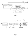
- a Roe comb filter is shown in Fig. 1.
- the filter comprises two one-line long delays 1 and 2.
- the samples at the ends of the delays and a sample in the middle thereof form a 1*3 window, from the centremost composite signal (lying between the delays) whereof the luminance signal Y and the chrominance signal C have to be separated, which chrominance signal can be divided further into the components U and V thereof.
- phase difference whereof is 180 degrees according to the PAL system
- the subtractor eliminates the phase difference of the signals, the result thereof after the averaging taking place in element 5 being a signal, being mostly of chrominance but having a 90 degree phase difference compared with the signal under study and residing between the delay lines. Said phase difference is eliminated and the incorrect PAL switch sense (the sign of the colour difference signal V) is inverted using a PAL modifier M.
- the modifier comprises a filter 6 for filtering the signal, unless it has been filtered earlier, as well as a mixer 7, the inputs whereof being the filtered chrominance signal and a sine signal with a frequency twice in magnitude of the frequency of the colour subcarrier.
- the phase of the signal to be obtained is determined by the phase of said sine frequency relative to the phase of the chrominance signal. From the mixing results of the mixer the frequencies are filtered off in the chrominance filter which are multiples of the subcarrier frequency. This results in a chrominance signal the switch sense of the V component whereof is inverted and into the phase of the U and V components whereof a 90 degree addition has been added.
- the signal derived from the bandpass filter 8 is the desired chrominance signal and the luminance signal Y is produced by subtracting from the composite signal the chrominance signal C in the subtractor 4.
- the comb filtering also causes cross chrominance and cross luminance.
- the cross luminance is seen e.g. in a TV test picture as a "running" of the luminance points occurring in the vicinity of the vertical edges of the colour bars in the TV test picture, while the cross chrominance is seen as extra colours on top of the parts of such picture, containing high horizontal luminance frequencies, such as in the black-and-white shirt of an ice hockey referee.
- errors are caused by a slight correlation between the delayed signals entering the filter when the combing crosses the horizontal colour edge.
- the combing with non-adaptive filters should not cross an edge like that, and various types of adaptive comb filters have been developed, one of their common features being that combing beyond the horizontal colour edge is avoided as much as possible. For this reason, an edge detector is needed in the filters.
- the chrominance signal produced by comb filtering is usually filtered with a narrow-band filter in order to reduce further the cross-chrominance. Unless no factor causing cross-chrominance exists, chrominance information becomes, however, lost unnecessarily in the narrow-band filter.
- control signal described in DE-A-3107736 although described for a colour coder, could in a similar way also be used in a colour decoder. However, the control signal described in DE-A-107736 was not designed for control on a pixel by pixel basis.
- GB-A-2 078 054 shows a PAL decoder with a sensor for detecting the presence of movement in the PAL signal. The sensor output is transformed into a control signal. This control signal is used for varying the effective signal combinations used to form the decoder output signals.
- the control signal described in GB-A-2 078 054 is not suitable for a control on a pixel by pixel basis.
- the object of the present invention is to provide a circuit arrangement by which the pixels can be detected in which cross chrominance might be produced in luminance-chrominance separation on a pixel by pixel basis also allowing a consistency check.
- a luminance signal Y from a Roe comb filter is carried to a bandpass filter, the average frequency thereof being approximately the same as the frequency of the colour subcarrier, whereby only the frequencies expected to produce cross chrominance transmit the filter.
- the filtered signal is then carried to a mixer where it is mixed with a colour subcarrier frequency signal.
- the frequencies above the zero frequency are filtered with a lowpass filter, whereby a low-frequency output signal proportional to the amount of cross-chrominance of a pixel is provided and checked for consistency on a pixel by pixel basis.
- a Roe line comb filter known in itself in the art is used so to separate the luminance and chrominance signals that all spatial luminance frequencies, also in the vicinity of the colour subcarrier frequency, remain.
- the filter causes aliasing at given luminance frequencies, visible as disturbing flickering in the picture being displayed.
- a chrominance signal provided by the Roe comb filter is filtered in a bandpass filter transmitting only the chrominance signal frequencies which would cause cross chrominance.
- the chrominance signal frequency thus filtered is transferred down into the vicinity of zero frequency, resulting in a low-frequency signal proportional to the amount of cross-chrominance. Said signal can thereafter be used for various controlling purposes of a comb filter or of a conventionally implemented filter.
- the low-frequency signal thus obtained should be filtered spatially because only the larger cross-chrominance areas show as disturbing.
- a signal representing the cross-chrominance of smaller areas can in such case be filtered off.
- Spatial filtering may be based on comparation and on a desired consistency check.
- the principle of a Roe comb filter as shown in Fig. 1 is described above.
- the Roe filter separates the luminance and chrominance signals so that all spatial luminance frequencies also in the vicinity of the colour subcarrier remain. However, certain diagonal edges at given luminance frequencies cause aliasing, which would be seen as flickering in the picture. Because of aliasing, the luminance signal of the Roe filter cannot be displayed as such on the screen, but because all luminance frequencies remain, the luminance signal can be used for detecting the luminance frequencies causing cross-chrominance.
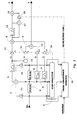
- FIG. 2 presents the principle diagram of the invention.
- a PAL composite signal is carried to the input of a Roe filter 21, which separates the chrominance and luminance signals in the manner of the description associated with Fig. 1.
- the filter 2 is thus the prior art filter shown in Fig. 1.
- a luminance signal Y from the Roe filter is filtered in a bandpass filter 22. If a comb filter is used in separating chrominance / luminance signals, the filter 22 can be identical with the actual chrominance bandpass filter used in the comb filter controlled by the displayed detector.
- the purpose of the filter 22 is to filter the luminance frequencies which cause no cross-chrominance, whereby a potential luminance signal causing cross-chrominance is obtained from the output of the filter.
- the signal provided by the filter is thereafter carried to a mixer 23 in which the signal is mixed down to the vicinity of zero frequency by mixing it into colour subcarrier frequency f sc , whereafter the extra high-frequency results are filtered from the mixing results with a lowpass filter 24, leaving a low-frequency signal proportional to the amount of cross-chrominance.
- the value of the signal is zero if no sample causing cross-chrominance exists, respectively, the value is above zero if the sample causes a cross error.
- This signal may already be used as such as one of the control signals of a filter, e.g. comb filter.
- a signal sample thus obtained in a non-linearity element 25 in which the sample is compared to a set threshold value.
- a threshold value By setting an appropriate threshold value, only the signals of desired magnitude can be conducted to the output of the circuit, whereby merely the signals causing disturbing cross-chrominance are included.
- a non-linearity element can be constructed so that the output is zero if the input is lower than the threshold value but when the input is greater than the threshold value, the output is equal to the input.
- a non-linearity element can be constructed so that the output thereof is "1" when the input is greater than the threshold value, but "0" when the input is smaller than the threshold value.
- the latter alternative can be implemented by means of a comparator.
- a consistency check of the sample thus obtained is carried out, for instance a spatial averaging. This can be implemented e.g. in an element operating in 3*3 window, the centremost pixel thereof being the pixel being studied.
- the averaging element 26 comprises at least two line memories, whereby a signal of the pixel, proportional to cross-chrominance detected in the manner described above, can be compared with an equivalent signal of the adjacent pixels, and finally, for the final output signal CC comparable to the cross-chrominance an average of the sample values of the window is taken.
- a signal CC comparable to the strength of the cross-chrominance can be produced.
- the signal can be used in a desired manner as one of the control signals of the comb filter, or, as described above, it can be used e.g. for adjusting the width of a chrominance bandpass in using a conventional low-pass (luminance) / bandpass (chrominance) filter arrangement for the separation.
- a conventional low-pass (luminance) / bandpass (chrominance) filter arrangement for the separation.
- the filter comprises an edge detection circuit 31, two one-line long delays 32 and 33 connected in succession, bandpass filters 35,36, a lowpass-suction filter combination 34, three adders 37,38,39, a subtractor 310, constant coefficients 315 and 316, and multipliers 311-314 controlled by the edge detection circuit.
- the mode of the filter is determined by the edge detection circuit 31. In a first mode, the coefficients 1-k of the multipliers 313 and 314 are given such values that the summing is not affected thereby in the adders 38 and 39, whereby signal C 1 becomes the chrominance signal for the output of the adder 38, and signal Y 1 becomes the luminance signal Y for the output of the adder 39.
- the chrominance signal C is produced by comb filtering from three vertically consecutive composite signals provided with the aid of the delay lines 32 and 33.
- the luminance signal is produced simply by subtracting the chrominance signal from the value of the centremost sample derived from between the delay lines in the subtraction circuit 310.
- the edge detection circuit If the existence of an edge is interpreted by the edge detection circuit, in other words, if the subsequent pixels of the vertical direction included in the combing are not sufficiently correlating, the other mode is used, i.e. the coefficients of the multipliers 311-314 are given such values that the chrominance signal C 2 becomes the output of the adder 38, and the luminance signal Y 2 becomes the output Y.
- the outputs of the filter can be glided between said two modes by gliding the values of the coefficients k and k-1 of the multipliers according to a control signal derived from the edge detection circuit 31.
- the invention can be e.g. so applied that a relatively narrow-banded bandpass filter 316, subtractor 317, multiplier 318 and adder 319 are inserted after the adder 38.
- the output of the subtractor 317 is formed by the chrominance frequencies which are filtered in the filter 316.
- the attenuation / amplification of multiplier 318 can be controlled, and so exert an influence on to what extent the frequency range is added in the output of the filter 316, i.e. a filter has been provided using the present circuit, in which the bandwidth can be changed.
- the amplification of the attenuator / amplifier 318 becomes adjusted to a maximum value, so that an ultimate chrominance signal C has been produced using the entire width of the band (the output signal C is in fact the same as the output signal of the adder 38). If the detector detects a strong cross-chrominance signal, the attenuation of the element 317 is adjusted to a maximum value, whereby no signal passes therefrom into the adder 319, and the output signal C has been provided from the narrow-band filter 316. The output C may therefore be controlled between said two extremes, depending on the detector control.
- the detector of the invention uses the detector of the invention to eliminate the picture errors caused by cross-chrominance almost completely.
- the detector is appropriate for use in association with any known comb filter in separating chrominance and luminance as well as in association with a circuit employing conventional lowpass (chrominance ) / bandpass (luminance) filtering in which a signal of the detector can be used e.g. for controlling the width of a chrominance bandpass.
- the detector can be implemented in a variety of ways while being included within the protective scope of the claims.
Landscapes
- Engineering & Computer Science (AREA)
- Multimedia (AREA)
- Signal Processing (AREA)
- Processing Of Color Television Signals (AREA)
Description
The control signal described in GB-A-2 078 054 is not suitable for a control on a pixel by pixel basis.
Claims (4)
- A circuit arrangement for detecting pixels causing cross-chrominance from a received sampled PAL composite video signal, said circuit arrangement comprising a comb filter (21) for separating colour difference signals and a luminance signal, comprisinga first line delay (1) connected in succession, to which an incoming PAL composite signal is conducted, and a second line delay (2), and a centre tap between said delays,a first subtractor (3), the inputs thereof being an incoming composite signal and an output signal of the second line delay (2),a PAL conversion element (6,7) to convert the polarity of the output signal of the first subtractor (3) to be equivalent to the polarity of a composite signal produced from the centre tap,a second subtractor (4), the inputs thereof being a composite signal from the centre tap and a filtered signal derived from the conversion element (6,7), and the output thereof being a luminance signal (Y) in which nearly all original spatial frequencies remain, characterized in that it further comprises:a bandpass filter (22) to the input of which the luminance signal (Y) is conducted and the centre frequency whereof is approximately the same as the frequency of the colour subcarrier, so that only the frequencies pass the filter which would cause cross-chrominance,a mixer (23), the input thereof being the output signal of the filter and the colour subcarrier frequency signal,a lowpass filter (24) to which the output signal of the mixer is conducted and which allows frequencies greater than the zero frequency from the mixing results to pass, thus forming an output signal which is a low-frequency signal indicative of the amount of cross-chrominance of the pixel,a comparator (25) to compare said low-frequency signal indicative of the amount of cross-chrominance with a predetermined threshold value and to maintain the output thereof at "zero" if said signal is below the threshold value or at "one" if said signal is above the threshold value,an element (26) for carrying out a consistency check to compare the output signal of the comparator with the equivalent signals indicative of the amount of cross-chrominance of the adjacent pixels and the output signal (CC) of which is a final signal indicative of the amount of cross-chrominance.
- Circuit arrangement according to claim 1, characterized in that the element carrying out the consistency check is a spatial averaging element.
- Circuit arrangement according to claim 2, characterized in that the element carrying out the spatial averaging is an element operating in a 3*3 window, calculating the average of the samples of the window.
- Circuit arrangement according to any one of the preceding claims, characterized in that a signal (CC) indicative of the amount of cross-chrominance is used e.g. for adjusting the bandwidth of a chrominance signal in separating the luminance and chrominance signals from the composite video signal.
Applications Claiming Priority (2)
| Application Number | Priority Date | Filing Date | Title |
|---|---|---|---|
| FI923741A FI92129C (en) | 1992-08-20 | 1992-08-20 | Switching arrangement for cross color detection |
| FI923741 | 1992-08-20 |
Publications (2)
| Publication Number | Publication Date |
|---|---|
| EP0586893A1 EP0586893A1 (en) | 1994-03-16 |
| EP0586893B1 true EP0586893B1 (en) | 1998-03-25 |
Family
ID=8535742
Family Applications (1)
| Application Number | Title | Priority Date | Filing Date |
|---|---|---|---|
| EP93112671A Expired - Lifetime EP0586893B1 (en) | 1992-08-20 | 1993-08-07 | Circuit arrangement for detecting cross colour |
Country Status (3)
| Country | Link |
|---|---|
| EP (1) | EP0586893B1 (en) |
| DE (1) | DE69317608T2 (en) |
| FI (1) | FI92129C (en) |
Family Cites Families (13)
| Publication number | Priority date | Publication date | Assignee | Title |
|---|---|---|---|---|
| US4167020A (en) * | 1977-12-12 | 1979-09-04 | Rca Corporation | Suppression of luminance signal contamination of chrominance signals in a video signal processing system |
| DE2821183C2 (en) * | 1978-05-13 | 1980-04-30 | Institut Fuer Rundfunktechnik Gmbh, 8000 Muenchen | Circuit arrangement for recognizing and possibly suppressing cross-color interference in color television signals |
| GB2078054B (en) * | 1980-06-02 | 1985-03-06 | British Broadcasting Corp | Pal decoding |
| DE3107736A1 (en) * | 1981-02-28 | 1982-09-16 | Robert Bosch Gmbh, 7000 Stuttgart | Method and circuit for suppressing interference by crosscolour |
| DE3107737A1 (en) * | 1981-02-28 | 1982-09-16 | Robert Bosch Gmbh, 7000 Stuttgart | Method and circuit for reducing interference by crosscolour |
| GB2124052B (en) * | 1982-05-06 | 1985-11-13 | Questech Ltd | Reducing cross-colour in colour television decoding apparatus |
| JPS6258795A (en) * | 1985-09-06 | 1987-03-14 | Mitsubishi Electric Corp | Pal system application type luminance signal and chrominance signal separating filter |
| US4688080A (en) * | 1985-09-27 | 1987-08-18 | Ampex Corporation | Multi-standard adaptive chrominance separator |
| DE3633716A1 (en) * | 1986-10-03 | 1988-04-14 | Bosch Gmbh Robert | Method and circuit for reducing interference due to cross-colour |
| US4814863A (en) * | 1987-06-09 | 1989-03-21 | Matsushita Electric Industrial Co., Ltd. | Detection and concealing artifacts in combed video signals |
| US4982271A (en) * | 1987-12-29 | 1991-01-01 | Victor Company Of Japan, Ltd. | Motion-adaptive device for separating luminance signal and color signal |
| DE3836043A1 (en) * | 1988-10-20 | 1990-04-26 | Thomson Brandt Gmbh | CIRCUIT FOR AN ADAPTIVE COMB FILTER FOR THE SEPARATION OF LUMINOUSITY SIGNAL AND COLOR TYPE SIGNAL OF AN FBAS-PAL SIGNAL |
| US5103296A (en) * | 1990-04-30 | 1992-04-07 | U.S. Philips Corporation | Color television system having adaptive filters in the transmitter encoder and in the receiver decoder |
-
1992
- 1992-08-20 FI FI923741A patent/FI92129C/en active IP Right Grant
-
1993
- 1993-08-07 DE DE69317608T patent/DE69317608T2/en not_active Expired - Fee Related
- 1993-08-07 EP EP93112671A patent/EP0586893B1/en not_active Expired - Lifetime
Non-Patent Citations (1)
| Title |
|---|
| Digital Television, C.P. Sandbank, JOHN WILEY & SONS * |
Also Published As
| Publication number | Publication date |
|---|---|
| FI923741A0 (en) | 1992-08-20 |
| EP0586893A1 (en) | 1994-03-16 |
| FI923741L (en) | 1994-02-21 |
| DE69317608T2 (en) | 1998-09-10 |
| FI92129C (en) | 1994-09-26 |
| DE69317608D1 (en) | 1998-04-30 |
| FI92129B (en) | 1994-06-15 |
Similar Documents
| Publication | Publication Date | Title |
|---|---|---|
| US4058836A (en) | Noise reduction in television signals | |
| US7474357B1 (en) | Decoding video signals to separate luma and chroma components | |
| US5519454A (en) | Luma/chroma separation filter with common delay element for comb filter separation and recursive noise reduction of composite video input signal | |
| CA1310401C (en) | Circuit for detecting motion of television signal | |
| GB2138243A (en) | Arrangement for the separation of the luminance and colour information of a colour television signal | |
| US4984068A (en) | Motion-adaptive device for separating luminance signal and color signal | |
| US5663771A (en) | Adaptive video comb filter with legalized output signals | |
| JP2571104B2 (en) | Apparatus for separating luminance and chrominance components | |
| US5063438A (en) | Three dimensional encoding system for color television | |
| EP0556501A1 (en) | Video motion detectors | |
| US4480266A (en) | Method and apparatus for preventing generation of false color signals in color television cameras | |
| US5225899A (en) | Correlation adaptive luminance and chrominance signal separating circuit | |
| US4775888A (en) | Motion detector for chrominance signal in TV receiver | |
| US4736252A (en) | Motion detector for chrominance signal in TV receiver | |
| US5365281A (en) | Motion signal detecting circuit | |
| US5548342A (en) | Luminance/chrominance separating circuit using predetermined separations | |
| EP0362747B1 (en) | Circuitry for comb filtering PAL and NTSC video signals | |
| EP0520311B1 (en) | Chrominance noise reduction apparatus employing two-dimensional recursive filtering of multiplexed baseband color difference components | |
| GB2283146A (en) | Adaptive chrominance and luminance separator | |
| EP0586893A1 (en) | Circuit arrangement for detecting cross colour | |
| GB2169772A (en) | Detecting horizontal colour changes in a video signal | |
| CA2100348A1 (en) | Colour television signal processing | |
| US6333764B1 (en) | Video signal luminance and chrominance separation | |
| JPH0338991A (en) | Luminance signal/color signal separation circuit | |
| JPH0638669B2 (en) | Motion detection circuit |
Legal Events
| Date | Code | Title | Description |
|---|---|---|---|
| PUAI | Public reference made under article 153(3) epc to a published international application that has entered the european phase |
Free format text: ORIGINAL CODE: 0009012 |
|
| AK | Designated contracting states |
Kind code of ref document: A1 Designated state(s): DE FR GB IT NL |
|
| 17P | Request for examination filed |
Effective date: 19940311 |
|
| 17Q | First examination report despatched |
Effective date: 19960326 |
|
| GRAG | Despatch of communication of intention to grant |
Free format text: ORIGINAL CODE: EPIDOS AGRA |
|
| GRAG | Despatch of communication of intention to grant |
Free format text: ORIGINAL CODE: EPIDOS AGRA |
|
| GRAG | Despatch of communication of intention to grant |
Free format text: ORIGINAL CODE: EPIDOS AGRA |
|
| GRAH | Despatch of communication of intention to grant a patent |
Free format text: ORIGINAL CODE: EPIDOS IGRA |
|
| GRAH | Despatch of communication of intention to grant a patent |
Free format text: ORIGINAL CODE: EPIDOS IGRA |
|
| GRAA | (expected) grant |
Free format text: ORIGINAL CODE: 0009210 |
|
| AK | Designated contracting states |
Kind code of ref document: B1 Designated state(s): DE FR GB IT NL |
|
| ITF | It: translation for a ep patent filed | ||
| REF | Corresponds to: |
Ref document number: 69317608 Country of ref document: DE Date of ref document: 19980430 |
|
| ET | Fr: translation filed | ||
| PLBE | No opposition filed within time limit |
Free format text: ORIGINAL CODE: 0009261 |
|
| 26N | No opposition filed | ||
| PGFP | Annual fee paid to national office [announced via postgrant information from national office to epo] |
Ref country code: NL Payment date: 20010830 Year of fee payment: 9 |
|
| REG | Reference to a national code |
Ref country code: GB Ref legal event code: IF02 |
|
| PGFP | Annual fee paid to national office [announced via postgrant information from national office to epo] |
Ref country code: GB Payment date: 20020807 Year of fee payment: 10 |
|
| PGFP | Annual fee paid to national office [announced via postgrant information from national office to epo] |
Ref country code: FR Payment date: 20020808 Year of fee payment: 10 |
|
| PGFP | Annual fee paid to national office [announced via postgrant information from national office to epo] |
Ref country code: DE Payment date: 20020816 Year of fee payment: 10 |
|
| PG25 | Lapsed in a contracting state [announced via postgrant information from national office to epo] |
Ref country code: NL Free format text: LAPSE BECAUSE OF NON-PAYMENT OF DUE FEES Effective date: 20030301 |
|
| NLV4 | Nl: lapsed or anulled due to non-payment of the annual fee |
Effective date: 20030301 |
|
| PG25 | Lapsed in a contracting state [announced via postgrant information from national office to epo] |
Ref country code: GB Free format text: LAPSE BECAUSE OF NON-PAYMENT OF DUE FEES Effective date: 20030807 |
|
| PG25 | Lapsed in a contracting state [announced via postgrant information from national office to epo] |
Ref country code: DE Free format text: LAPSE BECAUSE OF NON-PAYMENT OF DUE FEES Effective date: 20040302 |
|
| GBPC | Gb: european patent ceased through non-payment of renewal fee |
Effective date: 20030807 |
|
| PG25 | Lapsed in a contracting state [announced via postgrant information from national office to epo] |
Ref country code: FR Free format text: LAPSE BECAUSE OF NON-PAYMENT OF DUE FEES Effective date: 20040430 |
|
| REG | Reference to a national code |
Ref country code: FR Ref legal event code: ST |
|
| PG25 | Lapsed in a contracting state [announced via postgrant information from national office to epo] |
Ref country code: IT Free format text: LAPSE BECAUSE OF NON-PAYMENT OF DUE FEES;WARNING: LAPSES OF ITALIAN PATENTS WITH EFFECTIVE DATE BEFORE 2007 MAY HAVE OCCURRED AT ANY TIME BEFORE 2007. THE CORRECT EFFECTIVE DATE MAY BE DIFFERENT FROM THE ONE RECORDED. Effective date: 20050807 |