EP0585186A2 - Semiconductor insulation for optical devices - Google Patents
Semiconductor insulation for optical devices Download PDFInfo
- Publication number
- EP0585186A2 EP0585186A2 EP93420347A EP93420347A EP0585186A2 EP 0585186 A2 EP0585186 A2 EP 0585186A2 EP 93420347 A EP93420347 A EP 93420347A EP 93420347 A EP93420347 A EP 93420347A EP 0585186 A2 EP0585186 A2 EP 0585186A2
- Authority
- EP
- European Patent Office
- Prior art keywords
- enclosure
- integrated circuit
- substrate
- lens element
- die
- Prior art date
- Legal status (The legal status is an assumption and is not a legal conclusion. Google has not performed a legal analysis and makes no representation as to the accuracy of the status listed.)
- Granted
Links
Images


Classifications
-
- H—ELECTRICITY
- H10—SEMICONDUCTOR DEVICES; ELECTRIC SOLID-STATE DEVICES NOT OTHERWISE PROVIDED FOR
- H10H—INORGANIC LIGHT-EMITTING SEMICONDUCTOR DEVICES HAVING POTENTIAL BARRIERS
- H10H20/00—Individual inorganic light-emitting semiconductor devices having potential barriers, e.g. light-emitting diodes [LED]
- H10H20/80—Constructional details
- H10H20/85—Packages
- H10H20/855—Optical field-shaping means, e.g. lenses
-
- H—ELECTRICITY
- H04—ELECTRIC COMMUNICATION TECHNIQUE
- H04N—PICTORIAL COMMUNICATION, e.g. TELEVISION
- H04N23/00—Cameras or camera modules comprising electronic image sensors; Control thereof
- H04N23/50—Constructional details
- H04N23/54—Mounting of pick-up tubes, electronic image sensors, deviation or focusing coils
-
- H—ELECTRICITY
- H04—ELECTRIC COMMUNICATION TECHNIQUE
- H04N—PICTORIAL COMMUNICATION, e.g. TELEVISION
- H04N23/00—Cameras or camera modules comprising electronic image sensors; Control thereof
- H04N23/50—Constructional details
- H04N23/55—Optical parts specially adapted for electronic image sensors; Mounting thereof
-
- H—ELECTRICITY
- H10—SEMICONDUCTOR DEVICES; ELECTRIC SOLID-STATE DEVICES NOT OTHERWISE PROVIDED FOR
- H10F—INORGANIC SEMICONDUCTOR DEVICES SENSITIVE TO INFRARED RADIATION, LIGHT, ELECTROMAGNETIC RADIATION OF SHORTER WAVELENGTH OR CORPUSCULAR RADIATION
- H10F39/00—Integrated devices, or assemblies of multiple devices, comprising at least one element covered by group H10F30/00, e.g. radiation detectors comprising photodiode arrays
- H10F39/80—Constructional details of image sensors
- H10F39/804—Containers or encapsulations
-
- H—ELECTRICITY
- H10—SEMICONDUCTOR DEVICES; ELECTRIC SOLID-STATE DEVICES NOT OTHERWISE PROVIDED FOR
- H10F—INORGANIC SEMICONDUCTOR DEVICES SENSITIVE TO INFRARED RADIATION, LIGHT, ELECTROMAGNETIC RADIATION OF SHORTER WAVELENGTH OR CORPUSCULAR RADIATION
- H10F39/00—Integrated devices, or assemblies of multiple devices, comprising at least one element covered by group H10F30/00, e.g. radiation detectors comprising photodiode arrays
- H10F39/80—Constructional details of image sensors
- H10F39/806—Optical elements or arrangements associated with the image sensors
-
- H—ELECTRICITY
- H10—SEMICONDUCTOR DEVICES; ELECTRIC SOLID-STATE DEVICES NOT OTHERWISE PROVIDED FOR
- H10F—INORGANIC SEMICONDUCTOR DEVICES SENSITIVE TO INFRARED RADIATION, LIGHT, ELECTROMAGNETIC RADIATION OF SHORTER WAVELENGTH OR CORPUSCULAR RADIATION
- H10F77/00—Constructional details of devices covered by this subclass
- H10F77/40—Optical elements or arrangements
- H10F77/407—Optical elements or arrangements indirectly associated with the devices
-
- H—ELECTRICITY
- H10—SEMICONDUCTOR DEVICES; ELECTRIC SOLID-STATE DEVICES NOT OTHERWISE PROVIDED FOR
- H10F—INORGANIC SEMICONDUCTOR DEVICES SENSITIVE TO INFRARED RADIATION, LIGHT, ELECTROMAGNETIC RADIATION OF SHORTER WAVELENGTH OR CORPUSCULAR RADIATION
- H10F77/00—Constructional details of devices covered by this subclass
- H10F77/50—Encapsulations or containers
-
- H—ELECTRICITY
- H10—SEMICONDUCTOR DEVICES; ELECTRIC SOLID-STATE DEVICES NOT OTHERWISE PROVIDED FOR
- H10W—GENERIC PACKAGES, INTERCONNECTIONS, CONNECTORS OR OTHER CONSTRUCTIONAL DETAILS OF DEVICES COVERED BY CLASS H10
- H10W90/00—Package configurations
-
- Y—GENERAL TAGGING OF NEW TECHNOLOGICAL DEVELOPMENTS; GENERAL TAGGING OF CROSS-SECTIONAL TECHNOLOGIES SPANNING OVER SEVERAL SECTIONS OF THE IPC; TECHNICAL SUBJECTS COVERED BY FORMER USPC CROSS-REFERENCE ART COLLECTIONS [XRACs] AND DIGESTS
- Y10—TECHNICAL SUBJECTS COVERED BY FORMER USPC
- Y10S—TECHNICAL SUBJECTS COVERED BY FORMER USPC CROSS-REFERENCE ART COLLECTIONS [XRACs] AND DIGESTS
- Y10S174/00—Electricity: conductors and insulators
- Y10S174/35—Box or housing mounted on substrate or PCB
Definitions
- the present invention relates generally to encapsulating optically active electronic devices, more particularly to encapsulating such devices mounted on a printed circuit substrate within a pre-formed plastic enclosure having a unitary or a snap-in lens element in one wall thereof for focusing an image on or focusing light from the device.
- optically active integrated circuit (IC) die As electronic optical imaging systems become more compact, particularly with the incorporation of microelectronic photosensor elements for electronic auto exposure systems in relatively compact and inexpensive cameras, it has become desirable to mount the optically active integrated circuit (IC) die on a fiberglass printed circuit board or a ceramic substrate employing chip-on-board technology.
- IC optically active integrated circuit
- the mounting of the optically active IC die directly on or within a recess in a printed circuit board or a substrate allows the inter-connection with its associated circuitry and components to form a relatively compact, flat circuit assembly.
- the optically active semiconductor device is formed as an IC chip containing hundreds or thousands of separate semiconductor devices inter-connected with connection pads to which thin wires extending to printed circuit pads may be bonded.
- IC photosensitive IC
- the chip or die itself is characteristically small in size, with dimensions typically on the order of not more than 1/8" by 1/8" square by 0.015" thick.
- these chips in accordance with the prior art were typically packaged in supporting structures many times their size, such as in T0-5 cans with wire connection pins extending from the bottom thereof, flat packages with strip connectors extending from the edges thereof, and ceramic or plastic in-line packages with metal prongs extending out of the opposite edges and bent over to form a unit suitable for plugging into a socket or directly into apertures in a printed or hybrid circuit substrate.
- U.S. Patent No. 4,635,356 to Ohuchi et al. describes a method of encapsulating an electronic device wherein a large, free-form spacer is used as a barrier wall to surround electronic components mounted on a radiation-transparent support. The volume within the barrier wall is filled with a radiation curable material to form the finished device.
- a further U.S. patent number 4,054,938 to Morris describes the encapsulation of an integrated circuit chip or die.
- the die carrier is nested into an aperture in the substrate, and an encapsulation material dam provides a four sided enclosure wall placed in contacting engagement with the top surface of the substrate to surround the integrated circuit chip.
- a thermo-plastic epoxy material is placed over the chip and its attachment wires to pads on the substrate within the region confined by the dam.
- lens and windows mounted on separate packages for optically active integrated circuit chips where the chips or dies are mounted to substrates of the package, and the IC elements are electrically connected to terminal pins which in turn are inserted into connectors mounted to printed circuit boards or substrates.
- a miniaturized, flat and thin unitary electronic assembly comprising an integrated circuit chip or die (hereafter referred to collectively or individually as a die) mounted directly to a printed circuit board or hybrid circuit substrate (hereafter referred to collectively and individually as a printed circuit substrate) and provided with a protective lens assembly that is inexpensive and easy to assemble and provides accurate image focusing onto the optically active microelectronic circuit element(s) of the integrated circuit.
- One important object of the present invention is to thus provide a method and apparatus for assembling an optically active integrated circuit die directly to a printed circuit substrate within a protective, transparent enclosure having an imaging lens formed therein, such that, when assembled, the lens is accurately positioned with respect to the optically active elements of the integrated circuit die.
- an apparatus and method of enclosing an integrated circuit die mounted on a region of a printed circuit substrate of the type having conductive paths and connected components on at least one major surface thereof, the die having at least one optically active micro-electronic circuit element comprises the means for and steps of: forming a region on the substrate for receiving the integrated circuit die; attaching the integrated circuit die in the region so that the optically active integrated circuit elements are electrically connected to the conductive paths and are exposed to light; and attaching an enclosure to the substrate, the enclosure having a lens element formed in or assembled to a wall thereof and suspended over the optically active integrated circuit element and side alls surrounding the integrated circuit die within the region of the substrate to enclose and protect the die.
- a relatively flat and thin electronic circuit assembly is thus formed to enclose an integrated circuit chip or die attached directly to a printed circuit substrate comprising in combination: a printed circuit substrate having conductive paths and connected components on at least one major surface thereof arranged to terminate with connection pads of at least some of the paths spaced in a region of the substrate including an integrated circuit attachment site; an optically active integrated circuit die having at least one optically active circuit element adapted to respond to radiation impinging at least one surface thereof and a plurality of electrical terminal pads spaced thereon and a bottom surface; means for mechanically attaching the integrated circuit die to the site on the printed circuit substrate; means for electrically connecting the connection pads of the substrate to the terminal pads of the integrated circuit die; an integrated circuit enclosure and radiation focusing lens configured to enclose the integrated circuit die in the region of the printed circuit substrate; and means for mounting the enclosure and lens to the major surface of the printed circuit substrate such that the lens is focused on the optically active element of the integrated circuit die.
- the lens element and enclosure are formed integrally of an optically transparent material, e.g. glass or plastic.
- the enclosure is formed of an opaque material having a lens receiving aperture and the optically transmissive lens element is attached to the aperture of the enclosure.
- the means for and method of attaching further comprises filling the enclosed volume within the enclosure with a transparent sealing compound extending between the surface of the integrated circuit chip and the lens element in the top wall of the enclosure.
- a transparent sealing compound extending between the surface of the integrated circuit chip and the lens element in the top wall of the enclosure.
- the side walls have venting apertures for allowing excess sealing compound to escape.
- the means for and method of attaching further comprises a plurality of tab means extending into and engaging a like plurality of apertures in the printed circuit substrate, the tab means formed with catches to engage edges of the apertures and hold side wall edge surfaces of the side walls in contact with the surface of the substrate.
- locating pins extending from the edge surfaces of the side walls are preferably employed extending from the enclosure and through a further set of apertures in the printed circuit substrate to precisely locate and stabilize the enclosure during and following its attachment to the substrate.
- adhesive may be employed to seal the contact seam of the side wall edge surfaces and the substrate surface.
- the protective enclosure and lens comprises an optical plastic structure formed in a single piece having side walls adapted to be mounted against and extend from the substrate surface, the side walls having side wall edge surfaces and locating pins for supporting and suspending the lens element above the integrated circuit die and vents for releasing air displaced by sealing compound, and tabs for attaching the side wall edge surfaces of the plastic piece to the substrate surface whereby the plastic piece surrounds and encloses the region in which the integrated circuit die is mounted to the printed circuit substrate.
- the tabs preferably are formed with leading edge catches dimensioned to fit through the apertures in the printed circuit substrate for engaging the opposite surface of the printed circuit substrate in order to precisely position the lens element a fixed distance above the optically active surface of the integrated circuit die enclosed thereby.
- the receiving aperture for the lens element includes a seat and peripheral snap catches for engaging the annular edge of the lens element.
- the enclosure is first attached to the printed circuit substrate, optionally filled with a relatively low viscosity sealing compound, and the lens element is snapped into place against the seat and in contact with the sealing compound, if any.
- the lens element may displace sealing compound from the vents when the lens element is snapped in place. The sealing compound assists in holding all of the components in place.
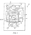
- Figure 1 is a top view of the assembly 10 of a printed circuit substrate 12, an integrated circuit (IC) die 14 and a protective, transparent, unitary lens and enclosure 15.
- Figure 1 is intended to illustrate the general relation of all of the elements of each of the preferred embodiments when assembled, but will be described, for convenience, in reference to the first embodiment of Figures 2-4.
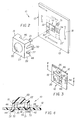
- Figure 2 illustrates the assembly 10 with the unitary lens and enclosure 15 suspended over and enclosing the region 17.
- the preferred embodiments of the enclosure 15 are molded of an optical plastic in a box-like shape having a lens element 20 in the top wall 22.
- the lens element 20 When assembled, as shown in Figures 3 and 4, the lens element 20 focuses an image onto the image receiving surface 24 of the IC die 14.
- the image receiving surface 24 may comprise one or more photosensitive microelectronic circuit elements.
- the printed circuit substrate 12 may comprise a thin sheet of ceramic or fiberglass material deposited or imprinted with a number of electrically conductive paths 16 that may be formed on the substrate 12 using any suitable process, for example by thick-film deposition when the substrate 12 comprises a ceramic, or by etching when the substrate comprises a fiberglass printed circuit board.
- the paths 16 may be attached to discrete electronic components 18 which may be either deposited to a ceramic substrate and trimmed in a manner well known in the art of hybrid circuit fabrication or may constitute discrete components having lead wires that are attached to the pads of the conductive paths 16 by ultrasonic welding or soldering in a manner well known in the art of assembling discrete components to printed circuit boards and ceramic substrates.
- the conductive paths 16 extend into and terminate within the region 17 outlined in Figure 2.
- the region 17 is surrounded by the "footprint" for the side wall edge surfaces 27 of the side walls 26 of the enclosure 15.
- the enclosure 15 is constructed with a pair of tabs 28 and 30 having tapered leading ends with notches and shoulders formed therein for insertion into apertures 32 and 34, respectively, formed in the printed circuit substrate 12.
- the IC die 14 is provided with a number of connector pads 36 arrayed on either side of the imaging receiving surface 24 that are adapted to be connected by lead wires 38 to miniaturized terminal pads 40 formed at the ends of the conductive paths 16 within the region 17.
- lead wires 38 comprise any suitable electrical conductors connected to the terminal pads 40 and connector pads 36 by any suitable bond.
- the conductors 38 can comprise ultrasonically bonded wires or soldered Tape Automated Bonding (TAB) leads.
- the other surface 25 of the IC die 14 is preferably cemented to the substrate surface 13 of the printed circuit substrate 12 at a predetermined site within the region 17 by applying a dab of adhesive having a negligible thickness thereto.
- Alternative methods of mounting the die 14 to the printed circuit substrate 12, e.g. in an aperture formed in the substrate 12, are described in the above-referenced '938 patent.
- the unitary lens and enclosure 15 is constructed with the convex lens element 20 extending superiorly of its top surface 22.
- the height of the side walls 26 and the shape of the lens element 22 are selected with respect to the thickness and positioning of the mounted IC die 14 in order to focus an image onto the photosensitive surface 24.
- the unitary transparent lens and enclosure 15 takes the place of the encapsulant and barrier described in the above incorporated '036 patent. The construction and principles of operation of the unitary lens and enclosure 15 are described in relation to the preferred embodiments thereof illustrated in Figures 3-6.
- Figure 3 and 4 they illustrate in an assembled perspective and a side elevation, cross-section view, respectively, the first embodiment of the attachment of the unitary lens and enclosure 15 by the insertion of the tabs 28 and 30 into the apertures 32 and 34, respectively, of the printed circuit substrate 12 in order to seat the side wall edge surfaces 27 against the substrate surface 13.
- the attachment is facilitated and the resulting assembly is strengthened by the positioning pins 21 and 23 that are fitted into pin receiving holes 31 and 33, respectively.
- the pins 21, 23 are somewhat longer than the tabs 28, 30.
- the pins 21, 23 provide positioning reference points since they must enter the holes 31, 33 before the tabs 28, 30 can enter and catch in the apertures 32, 34.
- the four point attachment provided by insertion of the pins 21, 23 and tabs 28, 30, into the respective holes 31, 33 and 32, 34 stabilizes the assembly and prevents accidental dislodgement of the lens and enclosure 15 in subsequent handling and manufacturing operations.
- the tabs 28 and 30 each extend from the top wall 22 of the lens and enclosure 15 in a flexible, leg-like manner and have a tapered edge catch 42 and 44, respectively, for engaging a surface of the printed circuit substrate 12 to lock the enclosure 15 in place.
- the enclosure 15 is positioned over the region 17, and the tabs 28 and 30 are pressed into the apertures 32 and 34 until the edge catches 42 and 44 snap into engagement with the edges of the apertures 32 and 34.
- the side wall edge surfaces 27 contact the substrate 12 in the region 17.
- the side walls 26 suspend the lens element 20 formed in the top wall 22 at a predetermined distance above the photosensitive surface 24 so that light from an image is focused by lens 20 onto the surface 24.
- the surfaces of the side walls 26 may be coated or painted with an opaque coating.
- FIGS 5-9 they illustrate views of a further embodiment of the invention wherein a discrete lens element 120 is constructed as a separate piece that is intended to be attached to an enclosure 115.
- the enclosure 115 is preferably formed of an opaque plastic that inhibits stray light from being inadvertently directed through the side walls 26 and onto the photosensitive surface 24.
- the centrally disposed discrete lens element 120 has an annular edge 121 that fits against an annular seat 128 formed in a lens element receptacle 122 and surrounding lens aperture 130 formed in the top wall 22.
- the receptacle 122 is formed with two flexible catches 124 and 126 that hold the edge 121 against the seat 128 and are associated with apertures 132 and 134 (visible in Figure 6).
- the enclosure 115 otherwise is constructed and assembled to the printed circuit substrate in the same manner as the first embodiment.
- the side wall edge surfaces 27 are four flat surfaces (visible in Figure 6) that bear against the substrate surface 13 in the four "footprints" 27' outlined around region 17 (shown in Figure 2). If it is deemed desirable to effect a stronger attachment, then it is contemplated that an adhesive material may be laid down in the footprints 27' around the region 17 on surface 13 of the substrate 12 that the side wall edge surfaces 27 contact. When assembled as depicted in Figures 3 and 7, the adhesive in the footprints of the side wall edge surfaces 27 and around the apertures 32, 34 and pin holes 31, 33 is compressed by the side wall edge surfaces 27 and squeezed out. Alternatively, in order to simplify manufacture, a fillet of adhesive 54 may be applied around the periphery of the side wall 26 and the surface 13 as shown for example in Figures 4 and 9.
- the snap-in attachment of the enclosures 15, 115 afforded by the above-described configuration of the tabs 28, 30 and positioning pins 21, 23 will be sufficient with or without adhesive to maintain the enclosure 15 in place for most applications.
- all or a portion of the interior volume 50 within the enclosures 15, 115 may be filled with an optically clear ultraviolet (UV) curable material, such as the dielectric polymer "NORLAND 63" available from NORLAND Products, Inc. or another suitable, optically transparent and colorless epoxy compound.
- UV optically clear ultraviolet
- the added encapsulant 52 further stabilizes the attachment of the die 14, wires 38 and enclosures 15, 115 and the discrete lens element 120 through its adhesion to each.
- the relatively viscous polymer would be deposited in a mass over the IC die 14 or into the volume 50 and compressed as shown in Figures 7 and 8 by the plastic enclosure 115 inserted over it. In this process, care must be taken to avoid the formation of bubbles or voids in the optical path between the lens 20, 120 and the photosensitive surface 24.
- vents 46 cut through a first pair of opposing side walls 26 and vents 48 cut through the other pair of opposing side walls 26. These vents allow trapped air to escape with a portion of the encapsulant 52 which seals the vents as shown in Figures 7 and 8, for example. In the second embodiment, a portion of the encapsulant may also enter the catch apertures 132 and 134 and contact a portion of the lens element edge 121. Although vents 46 and 48 are illustrated, it will be understood that solid side walls may be provided that seal the interior volume 50.
- lens elements are depicted in the top wall 22 of the enclosure 15, 115, it will be understood that the lens and suitable optical light guides or lens elements may be provided to orient the lens element into a side wall 26 to focus at right angles onto the photosensitive surface 24.
- IC die has been described as constituting a photosensitive semiconductor element or array of elements, it will be understood that the invention has application to other miniaturized optically active devices, including LED and other light and radiation emitting devices.
Landscapes
- Engineering & Computer Science (AREA)
- Multimedia (AREA)
- Signal Processing (AREA)
- Light Receiving Elements (AREA)
- Solid State Image Pick-Up Elements (AREA)
- Transforming Light Signals Into Electric Signals (AREA)
Abstract
Description
- The present invention relates generally to encapsulating optically active electronic devices, more particularly to encapsulating such devices mounted on a printed circuit substrate within a pre-formed plastic enclosure having a unitary or a snap-in lens element in one wall thereof for focusing an image on or focusing light from the device.
- As electronic optical imaging systems become more compact, particularly with the incorporation of microelectronic photosensor elements for electronic auto exposure systems in relatively compact and inexpensive cameras, it has become desirable to mount the optically active integrated circuit (IC) die on a fiberglass printed circuit board or a ceramic substrate employing chip-on-board technology. The mounting of the optically active IC die directly on or within a recess in a printed circuit board or a substrate allows the inter-connection with its associated circuitry and components to form a relatively compact, flat circuit assembly.
- Typically, the optically active semiconductor device is formed as an IC chip containing hundreds or thousands of separate semiconductor devices inter-connected with connection pads to which thin wires extending to printed circuit pads may be bonded. Such a photosensitive IC is disclosed in commonly assigned, U.S. Patent No. 5,037,198 to Gaboury and incorporated herein by reference. The chip or die itself is characteristically small in size, with dimensions typically on the order of not more than 1/8" by 1/8" square by 0.015" thick. Despite their small size, these chips in accordance with the prior art were typically packaged in supporting structures many times their size, such as in T0-5 cans with wire connection pins extending from the bottom thereof, flat packages with strip connectors extending from the edges thereof, and ceramic or plastic in-line packages with metal prongs extending out of the opposite edges and bent over to form a unit suitable for plugging into a socket or directly into apertures in a printed or hybrid circuit substrate.
- Regardless of the particular package utilized for prior art semiconductor chips, including CCD arrays, their primary drawback involves size and cost of separate packaging. On the other hand, the relatively small size packages provide protection from the environment and handling and allow for relatively fail-safe installation.
- In order to achieve miniaturization in the entire printed or hybrid circuit comprising the integrated circuit chips and the printed circuit board or substrate, various techniques have been proposed for eliminating the integrated circuit chip package, including mounting the chip or die directly on a prepared region of the substrate or board and encapsulating it in situ with various resins. In commonly assigned U.S. Patent No. 4,843,036, of which I am a named co-inventor, and with respect to Figure 1 of that patent, a method is described for encapsulating such optically active integrated
circuit chips 20 on asubstrate 10 using atransparent encapsulant 32 deposited- within a barrier formed around thechip 20. The encapsulant is deposited in a viscous state in the region contained within thebarrier 14 and thereafter is cured under ultraviolet light. The curedencapsulant 32 provides a functional, convex lens-like cross-sectional shape to provide focusing of light onto the optically active surface of the integrated device 20 (a photodiode in the disclosed embodiments). - The `036 patent also describes several prior art patents which describe methods for encapsulating electronic devices using radiation curable polymers. U.S. Patent No. 4,635,356 to Ohuchi et al. describes a method of encapsulating an electronic device wherein a large, free-form spacer is used as a barrier wall to surround electronic components mounted on a radiation-transparent support. The volume within the barrier wall is filled with a radiation curable material to form the finished device.
- A further U.S. patent number 4,054,938 to Morris describes the encapsulation of an integrated circuit chip or die. The die carrier is nested into an aperture in the substrate, and an encapsulation material dam provides a four sided enclosure wall placed in contacting engagement with the top surface of the substrate to surround the integrated circuit chip. A thermo-plastic epoxy material is placed over the chip and its attachment wires to pads on the substrate within the region confined by the dam.
- One difficulty encountered following the teachings of these references lies in the control of the shape of the curable resin or thermo-plastic epoxy material so that it consistently forms an optical lens suitably shaped to focus an image on the optically active integrated circuit. Earlier systems for enclosing optically active light detectors or light emitters have involved the incorporation of a transparent window or lens within the protective housing for the optically active semi-conductor device in a manner described, for example, in Japanese application number 58-115526 to Watabe, wherein a solid state image pick up device is provided within a package that itself is adapted to be attached to a printed circuit substrate in a manner described above. A lens element is fitted over the optically active surface of the solid-state pick up device and supported by the side walls of the package. Numerous other examples exist of lens and windows mounted on separate packages for optically active integrated circuit chips where the chips or dies are mounted to substrates of the package, and the IC elements are electrically connected to terminal pins which in turn are inserted into connectors mounted to printed circuit boards or substrates.
- It also is known from U.S. Patent Nos. 4,419,722 to Bury and 4,471,414 to Savage to provide snap-in assemblies for holding light emitting diodes (LEDs) in apertures provided in printed circuit boards to both protect and maintain the LED in its proper location.
- There remains a need for a miniaturized, flat and thin unitary electronic assembly comprising an integrated circuit chip or die (hereafter referred to collectively or individually as a die) mounted directly to a printed circuit board or hybrid circuit substrate (hereafter referred to collectively and individually as a printed circuit substrate) and provided with a protective lens assembly that is inexpensive and easy to assemble and provides accurate image focusing onto the optically active microelectronic circuit element(s) of the integrated circuit.
- One important object of the present invention is to thus provide a method and apparatus for assembling an optically active integrated circuit die directly to a printed circuit substrate within a protective, transparent enclosure having an imaging lens formed therein, such that, when assembled, the lens is accurately positioned with respect to the optically active elements of the integrated circuit die.
- In accordance with the invention, an apparatus and method of enclosing an integrated circuit die mounted on a region of a printed circuit substrate of the type having conductive paths and connected components on at least one major surface thereof, the die having at least one optically active micro-electronic circuit element, comprises the means for and steps of: forming a region on the substrate for receiving the integrated circuit die; attaching the integrated circuit die in the region so that the optically active integrated circuit elements are electrically connected to the conductive paths and are exposed to light; and attaching an enclosure to the substrate, the enclosure having a lens element formed in or assembled to a wall thereof and suspended over the optically active integrated circuit element and side alls surrounding the integrated circuit die within the region of the substrate to enclose and protect the die.
- In accordance with the present invention, a relatively flat and thin electronic circuit assembly is thus formed to enclose an integrated circuit chip or die attached directly to a printed circuit substrate comprising in combination: a printed circuit substrate having conductive paths and connected components on at least one major surface thereof arranged to terminate with connection pads of at least some of the paths spaced in a region of the substrate including an integrated circuit attachment site; an optically active integrated circuit die having at least one optically active circuit element adapted to respond to radiation impinging at least one surface thereof and a plurality of electrical terminal pads spaced thereon and a bottom surface; means for mechanically attaching the integrated circuit die to the site on the printed circuit substrate; means for electrically connecting the connection pads of the substrate to the terminal pads of the integrated circuit die; an integrated circuit enclosure and radiation focusing lens configured to enclose the integrated circuit die in the region of the printed circuit substrate; and means for mounting the enclosure and lens to the major surface of the printed circuit substrate such that the lens is focused on the optically active element of the integrated circuit die.
- In a first preferred embodiment, the lens element and enclosure are formed integrally of an optically transparent material, e.g. glass or plastic. In a second preferred embodiment, the enclosure is formed of an opaque material having a lens receiving aperture and the optically transmissive lens element is attached to the aperture of the enclosure.
- In a further embodiment, the means for and method of attaching further comprises filling the enclosed volume within the enclosure with a transparent sealing compound extending between the surface of the integrated circuit chip and the lens element in the top wall of the enclosure. Preferably, the side walls have venting apertures for allowing excess sealing compound to escape.
- In a still further embodiment, the means for and method of attaching further comprises a plurality of tab means extending into and engaging a like plurality of apertures in the printed circuit substrate, the tab means formed with catches to engage edges of the apertures and hold side wall edge surfaces of the side walls in contact with the surface of the substrate.
- In addition, locating pins extending from the edge surfaces of the side walls are preferably employed extending from the enclosure and through a further set of apertures in the printed circuit substrate to precisely locate and stabilize the enclosure during and following its attachment to the substrate.
- Optionally, adhesive may be employed to seal the contact seam of the side wall edge surfaces and the substrate surface.
- In the first preferred embodiment of the invention, the protective enclosure and lens comprises an optical plastic structure formed in a single piece having side walls adapted to be mounted against and extend from the substrate surface, the side walls having side wall edge surfaces and locating pins for supporting and suspending the lens element above the integrated circuit die and vents for releasing air displaced by sealing compound, and tabs for attaching the side wall edge surfaces of the plastic piece to the substrate surface whereby the plastic piece surrounds and encloses the region in which the integrated circuit die is mounted to the printed circuit substrate. The tabs preferably are formed with leading edge catches dimensioned to fit through the apertures in the printed circuit substrate for engaging the opposite surface of the printed circuit substrate in order to precisely position the lens element a fixed distance above the optically active surface of the integrated circuit die enclosed thereby.
- In the second preferred embodiment, the receiving aperture for the lens element includes a seat and peripheral snap catches for engaging the annular edge of the lens element. In use, the enclosure is first attached to the printed circuit substrate, optionally filled with a relatively low viscosity sealing compound, and the lens element is snapped into place against the seat and in contact with the sealing compound, if any. The lens element may displace sealing compound from the vents when the lens element is snapped in place. The sealing compound assists in holding all of the components in place.
- These and other advantages, objects and features of the invention will become apparent from the following description of the preferred embodiments of the invention in conjunction with the drawings in which:
- Figure 1 is a plan assembly view of an integrated circuit die attached to a site in a region of a printed circuit substrate and within a transparent, protective enclosure and lens element formed as a single piece;
- Figure 2 is an exploded perspective view of a first embodiment of the integral protective enclosure and the printed circuit substrate and integrated circuit die assembly of Figure 1;
- Figure 3 is an assembled perspective view of the embodiment of Figure 2;
- Figure 4 is a cross-section elevation view taken along lines A-A of Figure 3 depicting a first embodiment of the attachment of the protective enclosure to the printed circuit substrate;
- Figure 5 is an exploded, front perspective view of a second embodiment of the protective enclosure and the printed circuit substrate and integrated circuit die assembly of Figure 1;
- Figure 6 is an exploded, rear perspective view of the second embodiment of the protective enclosure and the printed circuit substrate and integrated circuit die assembly of Figure 1;
- Figure 7 is an assembled perspective view of the embodiment of Figures 5 and 6;
- Figure 8 is a cross-section elevation view taken along lines B-B of Figure 7 depicting a the attachment of the snap-in lens element to the protective enclosure and the protective enclosure to the printed circuit substrate; and
- Figure 9 is a cross-section elevation view taken along lines C-C of Figure 7.
- The drawings are not necessarily to scale.
- Turning now to the drawings of the preferred embodiments of the present invention, Figure 1 is a top view of the
assembly 10 of aprinted circuit substrate 12, an integrated circuit (IC) die 14 and a protective, transparent, unitary lens andenclosure 15. Figure 1 is intended to illustrate the general relation of all of the elements of each of the preferred embodiments when assembled, but will be described, for convenience, in reference to the first embodiment of Figures 2-4. - Figure 2 illustrates the
assembly 10 with the unitary lens andenclosure 15 suspended over and enclosing theregion 17. As shown in the cross-section views of Figure 4, the preferred embodiments of theenclosure 15 are molded of an optical plastic in a box-like shape having alens element 20 in thetop wall 22. When assembled, as shown in Figures 3 and 4, thelens element 20 focuses an image onto theimage receiving surface 24 of theIC die 14. As described in the above-incorporated `198 patent, theimage receiving surface 24 may comprise one or more photosensitive microelectronic circuit elements. - Returning to Figure 1, the printed
circuit substrate 12 may comprise a thin sheet of ceramic or fiberglass material deposited or imprinted with a number of electricallyconductive paths 16 that may be formed on thesubstrate 12 using any suitable process, for example by thick-film deposition when thesubstrate 12 comprises a ceramic, or by etching when the substrate comprises a fiberglass printed circuit board. Thepaths 16 may be attached to discreteelectronic components 18 which may be either deposited to a ceramic substrate and trimmed in a manner well known in the art of hybrid circuit fabrication or may constitute discrete components having lead wires that are attached to the pads of theconductive paths 16 by ultrasonic welding or soldering in a manner well known in the art of assembling discrete components to printed circuit boards and ceramic substrates. - The
conductive paths 16 extend into and terminate within theregion 17 outlined in Figure 2. Theregion 17 is surrounded by the "footprint" for the side wall edge surfaces 27 of theside walls 26 of theenclosure 15. Theenclosure 15 is constructed with a pair oftabs apertures circuit substrate 12. - The IC die 14 is provided with a number of
connector pads 36 arrayed on either side of theimaging receiving surface 24 that are adapted to be connected bylead wires 38 to miniaturized terminal pads 40 formed at the ends of theconductive paths 16 within theregion 17. It will be understood that thelead wires 38 comprise any suitable electrical conductors connected to the terminal pads 40 andconnector pads 36 by any suitable bond. For example, theconductors 38 can comprise ultrasonically bonded wires or soldered Tape Automated Bonding (TAB) leads. - The
other surface 25 of the IC die 14 is preferably cemented to thesubstrate surface 13 of the printedcircuit substrate 12 at a predetermined site within theregion 17 by applying a dab of adhesive having a negligible thickness thereto. Alternative methods of mounting the die 14 to the printedcircuit substrate 12, e.g. in an aperture formed in thesubstrate 12, are described in the above-referenced '938 patent. - The unitary lens and
enclosure 15 is constructed with theconvex lens element 20 extending superiorly of itstop surface 22. The height of theside walls 26 and the shape of thelens element 22 are selected with respect to the thickness and positioning of the mounted IC die 14 in order to focus an image onto thephotosensitive surface 24. In accordance with the present invention, the unitary transparent lens andenclosure 15 takes the place of the encapsulant and barrier described in the above incorporated '036 patent. The construction and principles of operation of the unitary lens andenclosure 15 are described in relation to the preferred embodiments thereof illustrated in Figures 3-6. - Turning now to Figure 3 and 4, they illustrate in an assembled perspective and a side elevation, cross-section view, respectively, the first embodiment of the attachment of the unitary lens and
enclosure 15 by the insertion of thetabs apertures circuit substrate 12 in order to seat the side wall edge surfaces 27 against thesubstrate surface 13. The attachment is facilitated and the resulting assembly is strengthened by the positioning pins 21 and 23 that are fitted intopin receiving holes pins tabs pins holes tabs apertures pins tabs respective holes enclosure 15 in subsequent handling and manufacturing operations. - The
tabs top wall 22 of the lens andenclosure 15 in a flexible, leg-like manner and have a taperededge catch circuit substrate 12 to lock theenclosure 15 in place. As shown in Figures 2-4, theenclosure 15 is positioned over theregion 17, and thetabs apertures apertures enclosure 15 is so attached, the side wall edge surfaces 27 contact thesubstrate 12 in theregion 17. Thus, theside walls 26 suspend thelens element 20 formed in thetop wall 22 at a predetermined distance above thephotosensitive surface 24 so that light from an image is focused bylens 20 onto thesurface 24. - In order to minimize the reflection of scattered light through the
side walls 26 and onto thesurface 24, either the inside or the outside, or both, the surfaces of theside walls 26 may be coated or painted with an opaque coating. - Turning to Figures 5-9, they illustrate views of a further embodiment of the invention wherein a
discrete lens element 120 is constructed as a separate piece that is intended to be attached to anenclosure 115. In this embodiment, theenclosure 115 is preferably formed of an opaque plastic that inhibits stray light from being inadvertently directed through theside walls 26 and onto thephotosensitive surface 24. The centrally disposeddiscrete lens element 120 has anannular edge 121 that fits against anannular seat 128 formed in alens element receptacle 122 and surroundinglens aperture 130 formed in thetop wall 22. Thereceptacle 122 is formed with twoflexible catches edge 121 against theseat 128 and are associated withapertures 132 and 134 (visible in Figure 6). Theenclosure 115 otherwise is constructed and assembled to the printed circuit substrate in the same manner as the first embodiment. - In both embodiments, the side wall edge surfaces 27 are four flat surfaces (visible in Figure 6) that bear against the
substrate surface 13 in the four "footprints" 27' outlined around region 17 (shown in Figure 2). If it is deemed desirable to effect a stronger attachment, then it is contemplated that an adhesive material may be laid down in the footprints 27' around theregion 17 onsurface 13 of thesubstrate 12 that the side wall edge surfaces 27 contact. When assembled as depicted in Figures 3 and 7, the adhesive in the footprints of the side wall edge surfaces 27 and around theapertures side wall 26 and thesurface 13 as shown for example in Figures 4 and 9. - It is contemplated that the snap-in attachment of the
enclosures tabs enclosure 15 in place for most applications. But in the further attachment embodiment also illustrated in Figures 7 and 8, all or a portion of theinterior volume 50 within theenclosures encapsulant 52 further stabilizes the attachment of the die 14,wires 38 andenclosures discrete lens element 120 through its adhesion to each. - In practice, the relatively viscous polymer would be deposited in a mass over the IC die 14 or into the
volume 50 and compressed as shown in Figures 7 and 8 by theplastic enclosure 115 inserted over it. In this process, care must be taken to avoid the formation of bubbles or voids in the optical path between thelens photosensitive surface 24. - The illustrated embodiments also show
vents 46 cut through a first pair of opposingside walls 26 and vents 48 cut through the other pair of opposingside walls 26. These vents allow trapped air to escape with a portion of theencapsulant 52 which seals the vents as shown in Figures 7 and 8, for example. In the second embodiment, a portion of the encapsulant may also enter thecatch apertures lens element edge 121. Althoughvents interior volume 50. - The use of the rigid, supported,
integral lens element 20 built into theenclosure 15 or theseparate lens element 120 snap attached to theenclosure 115 simplifies the manufacturing process and increases the yield of circuit assemblies having a properly focused lens element. - There are thus provided multiple embodiments for attaching the
enclosures substrate 12 for enclosing an optically active integrated circuit die mounted directly on or in the printed circuit substrate and having a lens element for focusing an image on the photosensitive surface of the die, which provide substantial improvements and advantages over the prior art. The above described and illustrated embodiments are intended to be illustrative of the principles of the present invention and not limited to the specific shape of the enclosure or the number and configuration of attachment mechanisms. - Moreover, while the lens elements are depicted in the
top wall 22 of theenclosure side wall 26 to focus at right angles onto thephotosensitive surface 24. - While IC die has been described as constituting a photosensitive semiconductor element or array of elements, it will be understood that the invention has application to other miniaturized optically active devices, including LED and other light and radiation emitting devices.
- While preferred embodiments of the invention have been illustrated and described, it will be clear that the invention is not so limited. Numerous modifications, changes, variations, substitutions, and equivalents will occur to those skilled in the art without departing from the spirit and scope of the present invention.
Claims (10)
- A method of enclosing an integrated circuit die mounted on a region of a printed circuit substrate of the type having conductive paths and connected components on at least one major surface thereof, the die having at least one optically active micro-electronic circuit element, comprising the steps of:
forming a region on the substrate for receiving the integrated circuit die;
attaching the integrated circuit die in the region so that the optically active integrated circuit elements are electrically connected to- the conductive paths and are exposed to light; and
attaching an enclosure to the substrate around the region, the enclosure having a lens element in a wall thereof suspended in optical focus with respect to the optically active integrated circuit element, the enclosure enclosing the integrated circuit die within the region of the substrate and protecting the die. - The method of Claim 1 wherein the attaching step further comprises the step of:
filling the enclosed volume within the enclosure with a transparent sealing compound extending between the surface of the integrated circuit die and the lens element in the wall of the enclosure. - Apparatus for enclosing and focusing light on or from an optically active integrated circuit die mounted on a region of a printed circuit substrate of the type having conductive paths and connected components on at least one major surface thereof, and attached so that the optically active integrated circuit elements are electrically connected to the conductive paths, comprising:
a lens element;
an enclosure for supporting the lens element in a wall thereof for focusing the lens element upon the optically active integrated circuit element, the enclosure having side walls; and
means for attaching the side walls of the enclosure to the substrate independently of the integrated circuit die and enclosing the integrated circuit die within the region of the substrate to protect the die. - The apparatus as defined in Claim 3 wherein the protective lens element and enclosure comprise an optical plastic structure formed in a unitary enclosure having the lens element formed in a top wall and side walls extending to side wall edge surfaces adapted to be mounted against the major surface of the printed circuit substrate, the side walls supporting and suspending the lens element above the integrated circuit die in optical focus with the optically active integrated circuit element.
- The apparatus as defined in Claim 3 wherein the enclosure further comprises :
a discrete lens element having an annular edge and an optical lens; and
a discrete supporting enclosure including the side wall attaching means and having a lens element receptacle means formed around an aperture in a wall thereof for receiving and retaining said lens element. - The apparatus as defined in Claim 5 wherein the lens element receptacle means further comprises :
an annular seat for receiving the annular edge; and locking means for holding the annular edge against the annular seat. - The apparatus as defined in any of Claims 3 to 6 wherein the attaching means further comprises:
encapsulant means filling the enclosed volume within the enclosure with a transparent sealing compound extending between the surface of the integrated circuit die and the lens element in the wall of the enclosure. - The apparatus as defined in any of Claims 3 to 7 wherein the enclosure side walls are provided with side wall edge surfaces and the attaching means further comprises:
a layer of adhesive between the side wall edge surfaces of the enclosure and the substrate surface. - The apparatus as defined in any of Claims 3 to 8 wherein the enclosure side walls are provided with side wall edge surfaces and the attaching means further comprises:
a plurality of tabs extending from the side walls of the enclosure and a like plurality of apertures in the substrate, the tabs having catches configured to engage the apertures and maintain the side wall edge surfaces in contact with the substrate surface. - The apparatus as defined in any of Claims 3 to 9 wherein the attaching means further comprises:
a plurality of positioning pins extending from the side wall edge surfaces of the enclosure; and
a like plurality of holes extending through the substrate in an arrangement configured to receive the plurality of positioning pins.
Applications Claiming Priority (2)
| Application Number | Priority Date | Filing Date | Title |
|---|---|---|---|
| US937791 | 1992-08-28 | ||
| US07/937,791 US5302778A (en) | 1992-08-28 | 1992-08-28 | Semiconductor insulation for optical devices |
Publications (3)
| Publication Number | Publication Date |
|---|---|
| EP0585186A2 true EP0585186A2 (en) | 1994-03-02 |
| EP0585186A3 EP0585186A3 (en) | 1995-02-08 |
| EP0585186B1 EP0585186B1 (en) | 1998-12-30 |
Family
ID=25470411
Family Applications (1)
| Application Number | Title | Priority Date | Filing Date |
|---|---|---|---|
| EP93420347A Expired - Lifetime EP0585186B1 (en) | 1992-08-28 | 1993-08-23 | Semiconductor insulation for optical devices |
Country Status (4)
| Country | Link |
|---|---|
| US (1) | US5302778A (en) |
| EP (1) | EP0585186B1 (en) |
| JP (1) | JP2559986B2 (en) |
| DE (1) | DE69322821T2 (en) |
Cited By (39)
| Publication number | Priority date | Publication date | Assignee | Title |
|---|---|---|---|---|
| WO1995034988A3 (en) * | 1994-06-14 | 1996-02-22 | Telepresence Systems Ltd | Miniature cameras |
| WO1997020344A1 (en) * | 1995-11-29 | 1997-06-05 | Telefonaktiebolaget Lm Ericsson (Publ) | A method and device for chip assembly |
| EP0901029A1 (en) * | 1997-09-06 | 1999-03-10 | Hella KG Hueck & Co. | Optical element |
| GB2352032A (en) * | 1999-07-16 | 2001-01-17 | Seiko Precision Kk | Optical detector with integrally moulded lens having a light blocking periphery |
| EP0773673A4 (en) * | 1995-05-31 | 2001-05-23 | Sony Corp | IMAGE INPUT DEVICE AND MANUFACTURING METHOD THEREOF, IMAGE INPUT ADAPTER, SIGNAL PROCESSOR, SIGNAL PROCESSING METHOD, INFORMATION PROCESSOR, AND INFORMATION PROCESSING METHOD |
| WO2001028234A3 (en) * | 1999-10-14 | 2001-06-07 | Bosch Gmbh Robert | Camera with an objective and a sensor |
| EP1223749A1 (en) * | 2001-01-12 | 2002-07-17 | Konica Corporation | Image pickup device and image pickup lens |
| FR2822326A1 (en) * | 2001-03-16 | 2002-09-20 | Atmel Grenoble Sa | LOW COST ELECTRONIC CAMERA IN INTEGRATED CIRCUIT TECHNOLOGY |
| WO2003107436A1 (en) * | 2002-06-12 | 2003-12-24 | Siemens Aktiengesellschaft | Optical module and optical system |
| EP1351496A3 (en) * | 2002-04-02 | 2004-01-07 | Konica Corporation | Producing method of image pickup device |
| EP1347637A3 (en) * | 2002-03-22 | 2004-01-07 | Konica Corporation | Image pickup device |
| EP1383175A1 (en) * | 2002-07-16 | 2004-01-21 | Abb Research Ltd. | Optoelectronic chip module |
| GB2391702A (en) * | 2002-06-07 | 2004-02-11 | Polymer Optics Ltd | Modular optical system |
| EP1429168A3 (en) * | 2002-12-13 | 2004-07-28 | Konica Minolta Holdings, Inc. | Image sensing device and portable terminal |
| DE10322757A1 (en) * | 2003-05-19 | 2004-12-30 | Infineon Technologies Ag | Optoelectronic transmission and / or reception arrangements |
| EP1465411A3 (en) * | 2003-03-31 | 2005-01-12 | Mitsumi Electric Co., Ltd. | Compact camera module |
| WO2004084317A3 (en) * | 2003-03-20 | 2005-02-17 | Firecomms Ltd | An optical sub-assembly for a transceiver |
| WO2004070839A3 (en) * | 2003-02-05 | 2005-03-10 | Acol Technologies S A | Light emitting apparatus comprising semiconductor light emitting devices |
| WO2005031879A1 (en) * | 2003-09-26 | 2005-04-07 | Siemens Aktiengesellschaft | Optical module and optical system |
| US6901029B2 (en) | 2001-03-30 | 2005-05-31 | Thales | Towed low-frequency underwater detection system |
| WO2005067281A1 (en) * | 2004-01-09 | 2005-07-21 | Robert Bosch Gmbh | Optical sensor device comprising an optical element at least partially integrated into the appliance housing |
| WO2006021179A1 (en) * | 2004-08-23 | 2006-03-02 | Osram Opto Semiconductors Gmbh | Device for an optoelectronic component and module with an optoelectronic component and a device |
| WO2006026372A1 (en) * | 2004-08-27 | 2006-03-09 | Tessera, Inc. | Package having integral lens and wafer-scale fabrication method therefor |
| WO2006012866A3 (en) * | 2004-07-28 | 2006-06-22 | Microelectronic Packaging Dres | Image module |
| EP0976589A4 (en) * | 1997-03-18 | 2006-11-08 | Acol Technologies S A | Luminescent diode |
| EP1498959A3 (en) * | 2003-07-18 | 2007-06-20 | Shinko Electric Industries Co., Ltd. | Manufacturing method of a semiconductor device |
| WO2007090694A1 (en) * | 2006-02-07 | 2007-08-16 | Continental Automotive Gmbh | Optical detection system |
| WO2007110255A1 (en) * | 2006-03-28 | 2007-10-04 | Robert Bosch Gmbh | Image recording system and method for production thereof |
| DE102006019717A1 (en) * | 2006-04-27 | 2007-10-31 | Siemens Ag | Optical module, has snap-in hook arranged in such a manner that surface of printed circuit board is aligned at definite preset distance with respect to optical lens in self adjustable manner |
| WO2009095091A1 (en) * | 2008-01-30 | 2009-08-06 | Sony Ericsson Mobile Communications Ab | Pin mounting of camera module |
| EP2069851A4 (en) * | 2006-09-14 | 2010-02-24 | Tessera Tech Hungary Kft | IMAGING SYSTEM WITH ASSOUPLY ASSEMBLED TOLERANCES AND ASSOCIATED METHODS |
| EP1624498A3 (en) * | 2004-08-03 | 2011-03-30 | Philips Lumileds Lighting Company LLC | Package for semiconductor light emitting device |
| WO2012041639A1 (en) * | 2010-09-30 | 2012-04-05 | Osram Ag | High temperature moldable lens, lighting device comprising lens and method making lighting device |
| AT14368U1 (en) * | 2013-07-23 | 2015-09-15 | Zumtobel Lighting Gmbh | LED lighting module |
| EP2944865A1 (en) * | 2012-12-18 | 2015-11-18 | LG Innotek Co., Ltd. | Lamp unit and vehicle lamp apparatus including the same |
| WO2016124184A1 (en) * | 2015-02-05 | 2016-08-11 | Conti Temic Microelectronic Gmbh | Camera module and method for the production thereof |
| EP3101699A1 (en) * | 2015-06-02 | 2016-12-07 | Radiall | Optoelectronic module for contactless optical link, related multi-channel modules, interconnection system, and associated method for manufacturing and connecting to a card |
| CN107534071A (en) * | 2015-04-27 | 2018-01-02 | 京瓷株式会社 | Light-receiving and light-emitting element module and sensor device |
| EP1864340B1 (en) * | 2005-02-28 | 2019-04-03 | OSRAM Opto Semiconductors GmbH | Illumination device |
Families Citing this family (100)
| Publication number | Priority date | Publication date | Assignee | Title |
|---|---|---|---|---|
| USD364603S (en) | 1994-06-20 | 1995-11-28 | Sanyo Electric Co., Ltd. | Light receiving module |
| USD373759S (en) | 1994-06-20 | 1996-09-17 | Sanyo Electric Co., Ltd. | Light receiving module |
| USD367848S (en) | 1994-06-30 | 1996-03-12 | Sony Corporation | Module for receiving infra-red signal of remote controller |
| USD364604S (en) | 1994-07-27 | 1995-11-28 | Sanyo Electric Co., Ltd. | Light receiving module |
| US6114097A (en) * | 1995-02-13 | 2000-09-05 | The Regents Of The University Of California | 3-D laser patterning process utilizing horizontal and vertical patterning |
| US6392703B1 (en) * | 1995-02-28 | 2002-05-21 | Canon Kabushiki Kaisha | Optical apparatus for forming an object image on a sensing element |
| USD390832S (en) | 1996-12-10 | 1998-02-17 | Elna Kabushiki Kaisha | Electronic device |
| JP3750276B2 (en) * | 1997-05-23 | 2006-03-01 | ソニー株式会社 | Method for mounting solid-state image sensor and method for mounting solid-state image sensor package |
| US7129978B1 (en) | 1998-07-13 | 2006-10-31 | Zoran Corporation | Method and architecture for an improved CMOS color image sensor |
| US6762796B1 (en) * | 1998-08-10 | 2004-07-13 | Olympus Optical Co., Ltd. | Image pickup module having integrated lens and semiconductor chip |
| US7133076B1 (en) * | 1998-12-24 | 2006-11-07 | Micron Technology, Inc. | Contoured surface cover plate for image sensor array |
| US6379991B2 (en) * | 1999-07-26 | 2002-04-30 | Micron Technology, Inc. | Encapsulation methods for semiconductive die packages |
| US7092031B1 (en) * | 1999-07-30 | 2006-08-15 | Zoran Corporation | Digital camera imaging module |
| WO2001015433A1 (en) * | 1999-08-19 | 2001-03-01 | Mitsubishi Denki Kabushiki Kaisha | Image pickup device and camera |
| US7176446B1 (en) | 1999-09-15 | 2007-02-13 | Zoran Corporation | Method and apparatus for distributing light onto electronic image sensors |
| US6483101B1 (en) | 1999-12-08 | 2002-11-19 | Amkor Technology, Inc. | Molded image sensor package having lens holder |
| JP3651577B2 (en) * | 2000-02-23 | 2005-05-25 | 三菱電機株式会社 | Imaging device |
| KR20030004353A (en) * | 2000-03-02 | 2003-01-14 | 올림파스 고가꾸 고교 가부시키가이샤 | Small-sized image pickup module |
| JP2001245217A (en) * | 2000-03-02 | 2001-09-07 | Olympus Optical Co Ltd | Small imaging module |
| JP2001257944A (en) * | 2000-03-10 | 2001-09-21 | Olympus Optical Co Ltd | Small imaging module |
| DE10032319A1 (en) * | 2000-07-04 | 2002-01-17 | Schneider Klaus | Fully-integrated wireless video and audio transmission system fitted directly in plug socket or via adapter module in light socket |
| US6525413B1 (en) | 2000-07-12 | 2003-02-25 | Micron Technology, Inc. | Die to die connection method and assemblies and packages including dice so connected |
| US7088397B1 (en) * | 2000-11-16 | 2006-08-08 | Avago Technologies General Ip Pte. Ltd | Image sensor packaging with imaging optics |
| JP4698874B2 (en) * | 2001-04-24 | 2011-06-08 | ローム株式会社 | Image sensor module and method of manufacturing image sensor module |
| US6598998B2 (en) * | 2001-05-04 | 2003-07-29 | Lumileds Lighting, U.S., Llc | Side emitting light emitting device |
| US6607286B2 (en) | 2001-05-04 | 2003-08-19 | Lumileds Lighting, U.S., Llc | Lens and lens cap with sawtooth portion for light emitting diode |
| JP2002341217A (en) * | 2001-05-14 | 2002-11-27 | Sony Corp | Imaging device and method of manufacturing the same |
| JP4033439B2 (en) * | 2001-09-11 | 2008-01-16 | シャープ株式会社 | Solid-state imaging unit, manufacturing method thereof, and imaging device |
| US7450862B2 (en) * | 2002-03-19 | 2008-11-11 | Axsun Technologies, Inc. | Stray light insensitive detector system and amplifier |
| JP3755149B2 (en) * | 2002-07-29 | 2006-03-15 | ミツミ電機株式会社 | Mounting the camera module on the board |
| CN100550430C (en) * | 2002-09-09 | 2009-10-14 | 皇家飞利浦电子股份有限公司 | Semiconductor device and method for manufacturing the same |
| US6896381B2 (en) * | 2002-10-11 | 2005-05-24 | Light Prescriptions Innovators, Llc | Compact folded-optics illumination lens |
| KR20040041930A (en) * | 2002-11-12 | 2004-05-20 | 삼성전기주식회사 | Lens assembly of camera module |
| US6924943B2 (en) * | 2002-12-02 | 2005-08-02 | Light Prescriptions Innovators, Llc | Asymmetric TIR lenses producing off-axis beams |
| US7042655B2 (en) * | 2002-12-02 | 2006-05-09 | Light Prescriptions Innovators, Llc | Apparatus and method for use in fulfilling illumination prescription |
| US7377671B2 (en) * | 2003-02-04 | 2008-05-27 | Light Prescriptions Innovators, Llc | Etendue-squeezing illumination optics |
| TWD113350S1 (en) | 2003-02-13 | 2006-10-11 | 夏普股份有限公司 | Infrared sensor |
| US7021797B2 (en) * | 2003-05-13 | 2006-04-04 | Light Prescriptions Innovators, Llc | Optical device for repositioning and redistributing an LED's light |
| US8075147B2 (en) * | 2003-05-13 | 2011-12-13 | Light Prescriptions Innovators, Llc | Optical device for LED-based lamp |
| US7329029B2 (en) * | 2003-05-13 | 2008-02-12 | Light Prescriptions Innovators, Llc | Optical device for LED-based lamp |
| JP3981348B2 (en) * | 2003-05-30 | 2007-09-26 | 松下電器産業株式会社 | Imaging device and manufacturing method thereof |
| EP1664851B1 (en) * | 2003-07-28 | 2014-11-12 | Light Prescriptions Innovators, LLC. | Three-dimensional simultaneous multiple-surface method and free-form illumination-optics designed therefrom |
| US7006306B2 (en) * | 2003-07-29 | 2006-02-28 | Light Prescriptions Innovators, Llc | Circumferentially emitting luminaires and lens-elements formed by transverse-axis profile-sweeps |
| US6934065B2 (en) * | 2003-09-18 | 2005-08-23 | Micron Technology, Inc. | Microelectronic devices and methods for packaging microelectronic devices |
| US6864116B1 (en) | 2003-10-01 | 2005-03-08 | Optopac, Inc. | Electronic package of photo-sensing semiconductor devices, and the fabrication and assembly thereof |
| US6943423B2 (en) * | 2003-10-01 | 2005-09-13 | Optopac, Inc. | Electronic package of photo-image sensors in cellular phone camera modules, and the fabrication and assembly thereof |
| US20050219033A1 (en) * | 2004-03-30 | 2005-10-06 | Sergio Bortolloni | Fuse status indicator for fuse cartridge |
| US7122874B2 (en) * | 2004-04-12 | 2006-10-17 | Optopac, Inc. | Electronic package having a sealing structure on predetermined area, and the method thereof |
| US6943424B1 (en) | 2004-05-06 | 2005-09-13 | Optopac, Inc. | Electronic package having a patterned layer on backside of its substrate, and the fabrication thereof |
| US7364934B2 (en) * | 2004-08-10 | 2008-04-29 | Micron Technology, Inc. | Microelectronic imaging units and methods of manufacturing microelectronic imaging units |
| US20060043513A1 (en) * | 2004-09-02 | 2006-03-02 | Deok-Hoon Kim | Method of making camera module in wafer level |
| KR100498708B1 (en) * | 2004-11-08 | 2005-07-01 | 옵토팩 주식회사 | Electronic package for semiconductor device and packaging method thereof |
| JP2006149462A (en) * | 2004-11-25 | 2006-06-15 | Olympus Corp | Device for acquiring information inside subject |
| US7473889B2 (en) * | 2004-12-16 | 2009-01-06 | Avago Technologies Ecbu Ip (Singapore) Pte. Ltd. | Optical integrated circuit package |
| US8393777B2 (en) * | 2005-07-28 | 2013-03-12 | Light Prescriptions Innovators, Llc | Etendue-conserving illumination-optics for backlights and frontlights |
| EP1920285A4 (en) * | 2005-07-28 | 2010-11-03 | Light Prescriptions Innovators | OPEN-FREE LENTICULAR OPTICAL ELEMENTS AND THEIR APPLICATION TO CAPACITORS AND PROJECTORS |
| WO2008008994A2 (en) * | 2006-07-14 | 2008-01-17 | Light Prescriptions Innovators, Llc | Brightness-enhancing film |
| JP2006350372A (en) * | 2006-07-24 | 2006-12-28 | Fujitsu Ltd | The camera module |
| KR101364997B1 (en) * | 2007-01-11 | 2014-02-19 | 삼성디스플레이 주식회사 | Backlight assembly and display device using the same |
| ATE553504T1 (en) * | 2007-02-20 | 2012-04-15 | Efw Inc | TEMPERATURE CONTROLLED PHOTO DETECTOR |
| DE102007038787B4 (en) * | 2007-08-06 | 2012-08-23 | Automotive Lighting Reutlingen Gmbh | Light module for a semiconductor light source lamp and semiconductor light source lamp |
| EP2195700A4 (en) * | 2007-10-01 | 2014-03-19 | Lighting Science Group Corp | Seven-cavity led array rgb collimation optic |
| US8269883B2 (en) * | 2008-01-10 | 2012-09-18 | Sharp Kabushiki Kaisha | Solid image capture device and electronic device incorporating same |
| US8218073B1 (en) * | 2008-01-25 | 2012-07-10 | Logitech Europe S.A. | Auto focus module for a webcam |
| JP4949289B2 (en) * | 2008-02-13 | 2012-06-06 | シャープ株式会社 | Solid-state imaging device and electronic apparatus including the same |
| EP2245364A2 (en) * | 2008-02-21 | 2010-11-03 | Light Prescriptions Innovators, LLC. | Spherically emitting remote phosphor |
| US8388193B2 (en) | 2008-05-23 | 2013-03-05 | Ruud Lighting, Inc. | Lens with TIR for off-axial light distribution |
| US9423096B2 (en) | 2008-05-23 | 2016-08-23 | Cree, Inc. | LED lighting apparatus |
| US8348475B2 (en) * | 2008-05-23 | 2013-01-08 | Ruud Lighting, Inc. | Lens with controlled backlight management |
| US8171625B1 (en) * | 2008-06-02 | 2012-05-08 | Wavefront Research, Inc. | Method of providing low footprint optical interconnect |
| TWI382796B (en) * | 2008-12-30 | 2013-01-11 | Au Optronics Corp | Method for manufacturing pcb, display module and fabricating method thereof |
| US10119662B2 (en) | 2009-04-28 | 2018-11-06 | Cree, Inc. | Lens with controlled light refraction |
| US9416926B2 (en) | 2009-04-28 | 2016-08-16 | Cree, Inc. | Lens with inner-cavity surface shaped for controlled light refraction |
| US9217854B2 (en) * | 2009-04-28 | 2015-12-22 | Cree, Inc. | Lens with controlled light refraction |
| US9255686B2 (en) | 2009-05-29 | 2016-02-09 | Cree, Inc. | Multi-lens LED-array optic system |
| US20110286120A1 (en) * | 2010-05-18 | 2011-11-24 | Harris William F | Optical lens snap attachment |
| DE102010030228B4 (en) | 2010-06-17 | 2018-06-07 | pmdtechnologies ag | Optical device |
| DE102011052793B4 (en) * | 2011-08-18 | 2013-11-07 | Sick Ag | optics carrier |
| US10408429B2 (en) | 2012-02-29 | 2019-09-10 | Ideal Industries Lighting Llc | Lens for preferential-side distribution |
| US9541258B2 (en) | 2012-02-29 | 2017-01-10 | Cree, Inc. | Lens for wide lateral-angle distribution |
| US9541257B2 (en) | 2012-02-29 | 2017-01-10 | Cree, Inc. | Lens for primarily-elongate light distribution |
| DE102012102627B4 (en) * | 2012-03-27 | 2016-06-09 | Leuze Electronic Gmbh & Co. Kg | optics holder |
| USD697664S1 (en) | 2012-05-07 | 2014-01-14 | Cree, Inc. | LED lens |
| KR102076339B1 (en) * | 2013-03-13 | 2020-02-11 | 삼성전자주식회사 | Semiconductor pakage and method of manufacturing the same |
| USD718490S1 (en) | 2013-03-15 | 2014-11-25 | Cree, Inc. | LED lens |
| US9523479B2 (en) | 2014-01-03 | 2016-12-20 | Cree, Inc. | LED lens |
| DE102014101787B4 (en) * | 2014-02-13 | 2021-10-28 | HELLA GmbH & Co. KGaA | Procedure for building an LED light module |
| DE102014104503B4 (en) * | 2014-03-31 | 2023-07-27 | HELLA GmbH & Co. KGaA | light system |
| US9478929B2 (en) * | 2014-06-23 | 2016-10-25 | Ken Smith | Light bulb receptacles and light bulb sockets |
| US9757912B2 (en) | 2014-08-27 | 2017-09-12 | Cree, Inc. | One-piece multi-lens optical member with ultraviolet inhibitor and method of manufacture |
| TWI600896B (en) * | 2015-07-08 | 2017-10-01 | 國立屏東科技大學 | Biochip detection assistant module |
| JP6660115B2 (en) | 2015-07-31 | 2020-03-04 | ソニーセミコンダクタソリューションズ株式会社 | Substrate with lens and method of manufacturing laminated lens structure |
| DE102015114563A1 (en) * | 2015-09-01 | 2017-03-02 | Osram Opto Semiconductors Gmbh | Microlens for LED module |
| DE102016000078B4 (en) | 2016-01-07 | 2023-08-17 | Ic-Haus Gmbh | Method of manufacturing an electronic assembly, electronic assembly and method of assembling an electronic assembly |
| DE102017105027A1 (en) * | 2017-03-09 | 2018-09-13 | Automotive Lighting Reutlingen Gmbh | Motor vehicle headlamps light module |
| US10468566B2 (en) | 2017-04-10 | 2019-11-05 | Ideal Industries Lighting Llc | Hybrid lens for controlled light distribution |
| DE102018207840A1 (en) * | 2018-05-18 | 2019-11-21 | Osram Gmbh | OPTICAL ARRANGEMENT AND HEADLIGHTS |
| CN114135808B (en) * | 2020-09-04 | 2024-06-11 | 英业达科技有限公司 | Assembling structure |
| EP3968466B1 (en) * | 2020-09-14 | 2025-06-25 | IXYS Semiconductor GmbH | Electrical contact for semiconductor package |
| US20240323503A1 (en) * | 2023-03-21 | 2024-09-26 | Zf Friedrichshafen Ag | Image sensor assembly |
Family Cites Families (33)
| Publication number | Priority date | Publication date | Assignee | Title |
|---|---|---|---|---|
| US3624462A (en) * | 1969-07-03 | 1971-11-30 | Fairchild Camera Instr Co | Face-bonded photoarray package |
| JPS5422115B2 (en) * | 1972-05-19 | 1979-08-04 | ||
| US4054938A (en) * | 1974-05-13 | 1977-10-18 | American Microsystems, Inc. | Combined semiconductor device and printed circuit board assembly |
| US3964157A (en) * | 1974-10-31 | 1976-06-22 | Bell Telephone Laboratories, Incorporated | Method of mounting semiconductor chips |
| US4143456A (en) * | 1976-06-28 | 1979-03-13 | Citizen Watch Commpany Ltd. | Semiconductor device insulation method |
| US4326214A (en) * | 1976-11-01 | 1982-04-20 | National Semiconductor Corporation | Thermal shock resistant package having an ultraviolet light transmitting window for a semiconductor chip |
| US4186995A (en) * | 1978-03-30 | 1980-02-05 | Amp Incorporated | Light device, lens, and fiber optic package |
| US4398240A (en) * | 1978-05-19 | 1983-08-09 | Savage John Jun | Lens cap holder for attachment to circuit boards |
| NL178376C (en) * | 1978-06-19 | 1986-03-03 | Philips Nv | COUPLING ELEMENT WITH A LIGHT SOURCE AND A LENS. |
| NL181963C (en) * | 1979-06-26 | 1987-12-01 | Philips Nv | SEMICONDUCTOR LASER DEVICE. |
| JPS56103484A (en) * | 1980-01-21 | 1981-08-18 | Fuji Photo Film Co Ltd | Manufacture of semiconductor device for photoelectric conversion |
| JPS56103481A (en) * | 1980-01-21 | 1981-08-18 | Fuji Photo Film Co Ltd | Manufacture of semiconductor device for photoelectric conversion |
| US4471414A (en) * | 1982-03-11 | 1984-09-11 | Savage John Jun | Integrated light unit and circuit element attachable to circuit board |
| US4419722A (en) * | 1982-05-07 | 1983-12-06 | Bury George J | Light emitting diode holder |
| US4491900A (en) * | 1982-09-27 | 1985-01-01 | Savage John Jun | Lens and mount for use with electromagnetic wave source |
| JPS607767A (en) * | 1983-06-27 | 1985-01-16 | Nec Corp | Semiconductor device |
| US4507718A (en) * | 1984-03-16 | 1985-03-26 | Illinois Tool Works Inc. | LED Holder |
| JPS612371A (en) * | 1984-06-14 | 1986-01-08 | Mitsubishi Electric Corp | Semiconductor photodetector |
| DE3503558A1 (en) * | 1985-02-02 | 1986-08-07 | Bosch Gmbh Robert | ENCLOSURE OF AT LEAST TWO PARTS |
| JPS6221282A (en) * | 1985-07-22 | 1987-01-29 | Nippon Telegr & Teleph Corp <Ntt> | Light conducting type detector |
| JPS62115750A (en) * | 1985-11-15 | 1987-05-27 | Nec Corp | Semiconductor device |
| FR2593930B1 (en) * | 1986-01-24 | 1989-11-24 | Radiotechnique Compelec | OPTO-ELECTRONIC DEVICE FOR SURFACE MOUNTING |
| US4843036A (en) * | 1987-06-29 | 1989-06-27 | Eastman Kodak Company | Method for encapsulating electronic devices |
| US4841100A (en) * | 1987-09-02 | 1989-06-20 | Minnesota Mining And Manufacturing Company | Expanding surface mount compatible retainer post |
| DE8717763U1 (en) * | 1987-12-24 | 1990-01-11 | Asea Brown Boveri Ag, 68309 Mannheim | Radiation detector |
| JPH01154639U (en) * | 1988-04-14 | 1989-10-24 | ||
| JP2682641B2 (en) * | 1988-06-03 | 1997-11-26 | 株式会社リコー | Semiconductor laser light source device |
| JPH0241188U (en) * | 1988-09-10 | 1990-03-22 | ||
| JPH0282056U (en) * | 1988-12-15 | 1990-06-25 | ||
| JPH02214169A (en) * | 1989-02-15 | 1990-08-27 | Fuji Photo Film Co Ltd | Semiconductor device |
| US4967262A (en) * | 1989-11-06 | 1990-10-30 | Micron Technology, Inc. | Gull-wing zig-zag inline lead package having end-of-package anchoring pins |
| CH680390A5 (en) * | 1990-05-18 | 1992-08-14 | Landis & Gyr Betriebs Ag | |
| US5037198A (en) * | 1990-07-16 | 1991-08-06 | Eastman Kodak Company | Illuminant discriminator with improved boundary conditions |
-
1992
- 1992-08-28 US US07/937,791 patent/US5302778A/en not_active Expired - Lifetime
-
1993
- 1993-08-23 EP EP93420347A patent/EP0585186B1/en not_active Expired - Lifetime
- 1993-08-23 DE DE69322821T patent/DE69322821T2/en not_active Expired - Fee Related
- 1993-08-30 JP JP5214381A patent/JP2559986B2/en not_active Expired - Lifetime
Cited By (68)
| Publication number | Priority date | Publication date | Assignee | Title |
|---|---|---|---|---|
| WO1995034988A3 (en) * | 1994-06-14 | 1996-02-22 | Telepresence Systems Ltd | Miniature cameras |
| EP0773673A4 (en) * | 1995-05-31 | 2001-05-23 | Sony Corp | IMAGE INPUT DEVICE AND MANUFACTURING METHOD THEREOF, IMAGE INPUT ADAPTER, SIGNAL PROCESSOR, SIGNAL PROCESSING METHOD, INFORMATION PROCESSOR, AND INFORMATION PROCESSING METHOD |
| EP1357741A1 (en) * | 1995-05-31 | 2003-10-29 | Sony Corporation | Image pickup apparatus |
| WO1997020344A1 (en) * | 1995-11-29 | 1997-06-05 | Telefonaktiebolaget Lm Ericsson (Publ) | A method and device for chip assembly |
| US6242274B1 (en) | 1995-11-29 | 2001-06-05 | Telefonaktiebolaget Lm Ericsson (Publ) | Method of mounting a chip on a flexible foil substrate for positioning on a capsule |
| EP0976589A4 (en) * | 1997-03-18 | 2006-11-08 | Acol Technologies S A | Luminescent diode |
| EP0901029A1 (en) * | 1997-09-06 | 1999-03-10 | Hella KG Hueck & Co. | Optical element |
| GB2352032B (en) * | 1999-07-16 | 2003-07-23 | Seiko Precision Kk | Optical detector |
| GB2352032A (en) * | 1999-07-16 | 2001-01-17 | Seiko Precision Kk | Optical detector with integrally moulded lens having a light blocking periphery |
| WO2001028234A3 (en) * | 1999-10-14 | 2001-06-07 | Bosch Gmbh Robert | Camera with an objective and a sensor |
| US7528880B2 (en) | 2001-01-12 | 2009-05-05 | Konica Corporation | Image pickup device and image pickup lens |
| US7880796B2 (en) | 2001-01-12 | 2011-02-01 | Konica Corporation | Image pickup device and image pickup lens |
| CN100473074C (en) * | 2001-01-12 | 2009-03-25 | 柯尼卡美能达精密光学株式会社 | Camera device and camera lens |
| EP1223749A1 (en) * | 2001-01-12 | 2002-07-17 | Konica Corporation | Image pickup device and image pickup lens |
| FR2822326A1 (en) * | 2001-03-16 | 2002-09-20 | Atmel Grenoble Sa | LOW COST ELECTRONIC CAMERA IN INTEGRATED CIRCUIT TECHNOLOGY |
| WO2002075815A1 (en) * | 2001-03-16 | 2002-09-26 | Atmel Grenoble S.A. | Low cost electronic camera made with integrated circuit technology |
| US6901029B2 (en) | 2001-03-30 | 2005-05-31 | Thales | Towed low-frequency underwater detection system |
| EP1347637A3 (en) * | 2002-03-22 | 2004-01-07 | Konica Corporation | Image pickup device |
| US6813103B2 (en) | 2002-04-02 | 2004-11-02 | Konica Corporation | Producing method of image pickup device |
| EP1351496A3 (en) * | 2002-04-02 | 2004-01-07 | Konica Corporation | Producing method of image pickup device |
| GB2391702B (en) * | 2002-06-07 | 2006-01-04 | Polymer Optics Ltd | Modular optical system |
| GB2391702A (en) * | 2002-06-07 | 2004-02-11 | Polymer Optics Ltd | Modular optical system |
| WO2003107436A1 (en) * | 2002-06-12 | 2003-12-24 | Siemens Aktiengesellschaft | Optical module and optical system |
| EP1383175A1 (en) * | 2002-07-16 | 2004-01-21 | Abb Research Ltd. | Optoelectronic chip module |
| EP1429168A3 (en) * | 2002-12-13 | 2004-07-28 | Konica Minolta Holdings, Inc. | Image sensing device and portable terminal |
| WO2004070839A3 (en) * | 2003-02-05 | 2005-03-10 | Acol Technologies S A | Light emitting apparatus comprising semiconductor light emitting devices |
| WO2004084317A3 (en) * | 2003-03-20 | 2005-02-17 | Firecomms Ltd | An optical sub-assembly for a transceiver |
| EP1686790A1 (en) * | 2003-03-31 | 2006-08-02 | Mitsumi Electric Co., Ltd. | Image pickup unit for compact camera module |
| US7515202B2 (en) | 2003-03-31 | 2009-04-07 | Mitsumi Electric Co., Ltd. | Compact camera module |
| EP1465411A3 (en) * | 2003-03-31 | 2005-01-12 | Mitsumi Electric Co., Ltd. | Compact camera module |
| US7223023B2 (en) | 2003-05-19 | 2007-05-29 | Infineon Technologies Ag | Optoelectronic transmission and/or reception arrangements |
| DE10322757A1 (en) * | 2003-05-19 | 2004-12-30 | Infineon Technologies Ag | Optoelectronic transmission and / or reception arrangements |
| DE10322757B4 (en) * | 2003-05-19 | 2012-08-30 | Avago Technologies Fiber Ip (Singapore) Pte. Ltd. | Optoelectronic transmitting and / or receiving arrangements |
| EP1498959A3 (en) * | 2003-07-18 | 2007-06-20 | Shinko Electric Industries Co., Ltd. | Manufacturing method of a semiconductor device |
| WO2005031879A1 (en) * | 2003-09-26 | 2005-04-07 | Siemens Aktiengesellschaft | Optical module and optical system |
| US7570439B2 (en) | 2003-09-26 | 2009-08-04 | Siemens Aktiengesellschaft | Optical module and optical system |
| WO2005067281A1 (en) * | 2004-01-09 | 2005-07-21 | Robert Bosch Gmbh | Optical sensor device comprising an optical element at least partially integrated into the appliance housing |
| WO2006012866A3 (en) * | 2004-07-28 | 2006-06-22 | Microelectronic Packaging Dres | Image module |
| EP1624498A3 (en) * | 2004-08-03 | 2011-03-30 | Philips Lumileds Lighting Company LLC | Package for semiconductor light emitting device |
| WO2006021179A1 (en) * | 2004-08-23 | 2006-03-02 | Osram Opto Semiconductors Gmbh | Device for an optoelectronic component and module with an optoelectronic component and a device |
| JP2008511143A (en) * | 2004-08-23 | 2008-04-10 | オスラム オプト セミコンダクターズ ゲゼルシャフト ミット ベシュレンクテル ハフツング | Device for optoelectronic component, and module comprising the optoelectronic component and device |
| US7948694B2 (en) | 2004-08-23 | 2011-05-24 | Osram Opto Semiconductor Gmbh | Apparatus for an optoelectronic device and componnent having an optoelectronic device and an apparatus |
| WO2006026372A1 (en) * | 2004-08-27 | 2006-03-09 | Tessera, Inc. | Package having integral lens and wafer-scale fabrication method therefor |
| EP1864340B1 (en) * | 2005-02-28 | 2019-04-03 | OSRAM Opto Semiconductors GmbH | Illumination device |
| EP2270888B1 (en) * | 2005-02-28 | 2019-10-23 | OSRAM Opto Semiconductors GmbH | Illumination device |
| WO2007090694A1 (en) * | 2006-02-07 | 2007-08-16 | Continental Automotive Gmbh | Optical detection system |
| CN101411179B (en) * | 2006-03-28 | 2011-09-14 | 罗伯特·博世有限公司 | Camera system and manufacturing method thereof |
| WO2007110255A1 (en) * | 2006-03-28 | 2007-10-04 | Robert Bosch Gmbh | Image recording system and method for production thereof |
| TWI386327B (en) * | 2006-03-28 | 2013-02-21 | 羅伯特博斯奇股份有限公司 | Image receiving system |
| US9742968B2 (en) | 2006-03-28 | 2017-08-22 | Robert Bosch Gmbh | Image acquisition system and method for the manufacture thereof |
| DE102006019717A1 (en) * | 2006-04-27 | 2007-10-31 | Siemens Ag | Optical module, has snap-in hook arranged in such a manner that surface of printed circuit board is aligned at definite preset distance with respect to optical lens in self adjustable manner |
| EP2069851A4 (en) * | 2006-09-14 | 2010-02-24 | Tessera Tech Hungary Kft | IMAGING SYSTEM WITH ASSOUPLY ASSEMBLED TOLERANCES AND ASSOCIATED METHODS |
| US8159602B2 (en) | 2006-09-14 | 2012-04-17 | DigitalOptics Corporation Europe Limited | Imaging system with relaxed assembly tolerances and associated methods |
| US7966041B2 (en) | 2008-01-30 | 2011-06-21 | Sony Ericsson Mobile Communications Ab | Pin mounting of camera module in a radio communication terminal |
| WO2009095091A1 (en) * | 2008-01-30 | 2009-08-06 | Sony Ericsson Mobile Communications Ab | Pin mounting of camera module |
| US9447943B2 (en) | 2010-09-30 | 2016-09-20 | Osram Gmbh | High temperature moldable lens, lighting device comprising lens and method making lighting device |
| WO2012041639A1 (en) * | 2010-09-30 | 2012-04-05 | Osram Ag | High temperature moldable lens, lighting device comprising lens and method making lighting device |
| US9671069B2 (en) | 2012-12-18 | 2017-06-06 | Lg Innotek Co., Ltd. | Lamp unit and vehicle lamp apparatus including the same |
| EP2944865A1 (en) * | 2012-12-18 | 2015-11-18 | LG Innotek Co., Ltd. | Lamp unit and vehicle lamp apparatus including the same |
| US9970627B2 (en) | 2012-12-18 | 2018-05-15 | Lg Innotek Co., Ltd. | Lamp unit and vehicle lamp apparatus including the same |
| AT14368U1 (en) * | 2013-07-23 | 2015-09-15 | Zumtobel Lighting Gmbh | LED lighting module |
| WO2016124184A1 (en) * | 2015-02-05 | 2016-08-11 | Conti Temic Microelectronic Gmbh | Camera module and method for the production thereof |
| CN107534071A (en) * | 2015-04-27 | 2018-01-02 | 京瓷株式会社 | Light-receiving and light-emitting element module and sensor device |
| EP3291313A4 (en) * | 2015-04-27 | 2019-01-09 | Kyocera Corporation | LIGHT RECEIVING AND TRANSMITTING ELEMENT MODULE AND SENSOR DEVICE |
| US10374116B2 (en) | 2015-04-27 | 2019-08-06 | Kyocera Corporation | Light receiving and emitting element module and sensor device |
| EP3101699A1 (en) * | 2015-06-02 | 2016-12-07 | Radiall | Optoelectronic module for contactless optical link, related multi-channel modules, interconnection system, and associated method for manufacturing and connecting to a card |
| FR3037190A1 (en) * | 2015-06-02 | 2016-12-09 | Radiall Sa | OPTOELECTRONIC MODULE FOR MECHANICAL CONTACTLESS OPTICAL LINK, MODULE ASSEMBLY, INTERCONNECTION SYSTEM, METHOD FOR MAKING AND CONNECTING TO AN ASSOCIATED CARD |
| US10337913B2 (en) | 2015-06-02 | 2019-07-02 | Radiall | Optoelectronic module for a contactless free-space optical link, associated multichannel modules, associated interconnection system, method of production and connection to a board |
Also Published As
| Publication number | Publication date |
|---|---|
| EP0585186A3 (en) | 1995-02-08 |
| JP2559986B2 (en) | 1996-12-04 |
| DE69322821T2 (en) | 1999-07-08 |
| JPH06177271A (en) | 1994-06-24 |
| DE69322821D1 (en) | 1999-02-11 |
| EP0585186B1 (en) | 1998-12-30 |
| US5302778A (en) | 1994-04-12 |
Similar Documents
| Publication | Publication Date | Title |
|---|---|---|
| US5302778A (en) | Semiconductor insulation for optical devices | |
| JP3507251B2 (en) | Optical sensor IC package and method of assembling the same | |
| US7791184B2 (en) | Image sensor packages and frame structure thereof | |
| EP0561964B1 (en) | Optoelectronic device component package and method of making the same | |
| US8097895B2 (en) | Electronic device package with an optical device | |
| KR101120341B1 (en) | Solide imaging device and manufacturing method thereof | |
| US20030136968A1 (en) | Semiconductor package having light sensitive chips | |
| WO2001091193A2 (en) | Integrated ic chip package for electronic image sensor die | |
| KR20090104020A (en) | Housing for optoelectronic devices and placement of optoelectronic devices in the housing | |
| CN101159279A (en) | Semiconductor imaging element and manufacturing method thereof, semiconductor imaging element module and device | |
| US5216805A (en) | Method of manufacturing an optoelectronic device package | |
| EP0690515A1 (en) | Optoelectronic assembly and methods for producing and using the same | |
| JPH08116095A (en) | Light emitting device | |
| JP3585952B2 (en) | Optical coupling device | |
| JP2004253455A (en) | Semiconductor device and method of manufacturing the same |
Legal Events
| Date | Code | Title | Description |
|---|---|---|---|
| PUAI | Public reference made under article 153(3) epc to a published international application that has entered the european phase |
Free format text: ORIGINAL CODE: 0009012 |
|
| AK | Designated contracting states |
Kind code of ref document: A2 Designated state(s): DE FR GB |
|
| PUAL | Search report despatched |
Free format text: ORIGINAL CODE: 0009013 |
|
| AK | Designated contracting states |
Kind code of ref document: A3 Designated state(s): DE FR GB |
|
| 17P | Request for examination filed |
Effective date: 19950718 |
|
| 17Q | First examination report despatched |
Effective date: 19950821 |
|
| GRAG | Despatch of communication of intention to grant |
Free format text: ORIGINAL CODE: EPIDOS AGRA |
|
| GRAG | Despatch of communication of intention to grant |
Free format text: ORIGINAL CODE: EPIDOS AGRA |
|
| GRAH | Despatch of communication of intention to grant a patent |
Free format text: ORIGINAL CODE: EPIDOS IGRA |
|
| GRAH | Despatch of communication of intention to grant a patent |
Free format text: ORIGINAL CODE: EPIDOS IGRA |
|
| GRAA | (expected) grant |
Free format text: ORIGINAL CODE: 0009210 |
|
| AK | Designated contracting states |
Kind code of ref document: B1 Designated state(s): DE FR GB |
|
| REF | Corresponds to: |
Ref document number: 69322821 Country of ref document: DE Date of ref document: 19990211 |
|
| ET | Fr: translation filed | ||
| PLBE | No opposition filed within time limit |
Free format text: ORIGINAL CODE: 0009261 |
|
| STAA | Information on the status of an ep patent application or granted ep patent |
Free format text: STATUS: NO OPPOSITION FILED WITHIN TIME LIMIT |
|
| 26N | No opposition filed | ||
| REG | Reference to a national code |
Ref country code: GB Ref legal event code: IF02 |
|
| PGFP | Annual fee paid to national office [announced via postgrant information from national office to epo] |
Ref country code: GB Payment date: 20050707 Year of fee payment: 13 |
|
| PGFP | Annual fee paid to national office [announced via postgrant information from national office to epo] |
Ref country code: FR Payment date: 20050804 Year of fee payment: 13 |
|
| PGFP | Annual fee paid to national office [announced via postgrant information from national office to epo] |
Ref country code: DE Payment date: 20050831 Year of fee payment: 13 |
|
| PG25 | Lapsed in a contracting state [announced via postgrant information from national office to epo] |
Ref country code: DE Free format text: LAPSE BECAUSE OF NON-PAYMENT OF DUE FEES Effective date: 20070301 |
|
| GBPC | Gb: european patent ceased through non-payment of renewal fee |
Effective date: 20060823 |
|
| REG | Reference to a national code |
Ref country code: FR Ref legal event code: ST Effective date: 20070430 |
|
| PG25 | Lapsed in a contracting state [announced via postgrant information from national office to epo] |
Ref country code: GB Free format text: LAPSE BECAUSE OF NON-PAYMENT OF DUE FEES Effective date: 20060823 |
|
| PG25 | Lapsed in a contracting state [announced via postgrant information from national office to epo] |
Ref country code: FR Free format text: LAPSE BECAUSE OF NON-PAYMENT OF DUE FEES Effective date: 20060831 |