EP0584777A1 - Semiconductor device and process for producing the same - Google Patents
Semiconductor device and process for producing the same Download PDFInfo
- Publication number
- EP0584777A1 EP0584777A1 EP93113472A EP93113472A EP0584777A1 EP 0584777 A1 EP0584777 A1 EP 0584777A1 EP 93113472 A EP93113472 A EP 93113472A EP 93113472 A EP93113472 A EP 93113472A EP 0584777 A1 EP0584777 A1 EP 0584777A1
- Authority
- EP
- European Patent Office
- Prior art keywords
- porous
- semiconductor device
- region
- regions
- wafer
- Prior art date
- Legal status (The legal status is an assumption and is not a legal conclusion. Google has not performed a legal analysis and makes no representation as to the accuracy of the status listed.)
- Granted
Links
Images


Classifications
-
- H—ELECTRICITY
- H01—ELECTRIC ELEMENTS
- H01L—SEMICONDUCTOR DEVICES NOT COVERED BY CLASS H10
- H01L33/00—Semiconductor devices with at least one potential-jump barrier or surface barrier specially adapted for light emission; Processes or apparatus specially adapted for the manufacture or treatment thereof or of parts thereof; Details thereof
- H01L33/02—Semiconductor devices with at least one potential-jump barrier or surface barrier specially adapted for light emission; Processes or apparatus specially adapted for the manufacture or treatment thereof or of parts thereof; Details thereof characterised by the semiconductor bodies
- H01L33/26—Materials of the light emitting region
- H01L33/34—Materials of the light emitting region containing only elements of group IV of the periodic system
- H01L33/346—Materials of the light emitting region containing only elements of group IV of the periodic system containing porous silicon
-
- G—PHYSICS
- G01—MEASURING; TESTING
- G01N—INVESTIGATING OR ANALYSING MATERIALS BY DETERMINING THEIR CHEMICAL OR PHYSICAL PROPERTIES
- G01N27/00—Investigating or analysing materials by the use of electric, electrochemical, or magnetic means
- G01N27/02—Investigating or analysing materials by the use of electric, electrochemical, or magnetic means by investigating impedance
- G01N27/04—Investigating or analysing materials by the use of electric, electrochemical, or magnetic means by investigating impedance by investigating resistance
- G01N27/12—Investigating or analysing materials by the use of electric, electrochemical, or magnetic means by investigating impedance by investigating resistance of a solid body in dependence upon absorption of a fluid; of a solid body in dependence upon reaction with a fluid, for detecting components in the fluid
-
- H—ELECTRICITY
- H01—ELECTRIC ELEMENTS
- H01L—SEMICONDUCTOR DEVICES NOT COVERED BY CLASS H10
- H01L21/00—Processes or apparatus adapted for the manufacture or treatment of semiconductor or solid state devices or of parts thereof
- H01L21/02—Manufacture or treatment of semiconductor devices or of parts thereof
- H01L21/04—Manufacture or treatment of semiconductor devices or of parts thereof the devices having at least one potential-jump barrier or surface barrier, e.g. PN junction, depletion layer or carrier concentration layer
- H01L21/18—Manufacture or treatment of semiconductor devices or of parts thereof the devices having at least one potential-jump barrier or surface barrier, e.g. PN junction, depletion layer or carrier concentration layer the devices having semiconductor bodies comprising elements of Group IV of the Periodic System or AIIIBV compounds with or without impurities, e.g. doping materials
- H01L21/30—Treatment of semiconductor bodies using processes or apparatus not provided for in groups H01L21/20 - H01L21/26
- H01L21/302—Treatment of semiconductor bodies using processes or apparatus not provided for in groups H01L21/20 - H01L21/26 to change their surface-physical characteristics or shape, e.g. etching, polishing, cutting
- H01L21/306—Chemical or electrical treatment, e.g. electrolytic etching
-
- Y—GENERAL TAGGING OF NEW TECHNOLOGICAL DEVELOPMENTS; GENERAL TAGGING OF CROSS-SECTIONAL TECHNOLOGIES SPANNING OVER SEVERAL SECTIONS OF THE IPC; TECHNICAL SUBJECTS COVERED BY FORMER USPC CROSS-REFERENCE ART COLLECTIONS [XRACs] AND DIGESTS
- Y10—TECHNICAL SUBJECTS COVERED BY FORMER USPC
- Y10S—TECHNICAL SUBJECTS COVERED BY FORMER USPC CROSS-REFERENCE ART COLLECTIONS [XRACs] AND DIGESTS
- Y10S438/00—Semiconductor device manufacturing: process
- Y10S438/96—Porous semiconductor
Definitions
- the present invention relates to a semiconductor device such as an electronic element, an optical element, and integrated circuit thereof which performs functions of light-emission, sensing, or the like, and also relates to a process for producing the semiconductor device.
- the present invention relates to a semiconductor device having a porous region and to a process for producing the device.
- Porous materials are attracting attention in recent years as a novel functional material for constituting an active region of an element.
- the porous structure of semiconductor crystal of Group IV were mainly used in the past as structural members which are not related to the electronic and optical properties of the material: the uses such as formation of SOI (Silicon On Insulator) structure utilizing capability of high speed oxidation (see, for example, T. Unagami and M. Seki: J. Electrochem. Soc., 125, 1339 (1978)).
- SOI Silicon On Insulator
- the porous material is applied to an active region material of a gas sensor by utilizing the large surface area resulting from the porosity (see, for example, A. Motohashi, et al.: Oyo Butsuri Gakkai Gakujutsu Koenkai (Shuki) Yokoshu (Preprint of Autumnal Meeting of Society of Applied Physics), 29p-ZB-9 (1986)); and light-emission phenomenon was discovered which is caused by a structure sufficiently fine for imprisonment of carrier quantum (see L.T. Canham, Appl. Phys. Lett., 56, 1046 (1990)). Since then, studies are being made actively on functional application of porous material to light-emitting element, and other applications. The functional application of the porous material will possibly become an attractive novel technique if several practical problems are solved, because the porous structure can be formed readily by treating the base material.
- the porous material as understood from the name, has many voids in the space where the material is to be filled inherently. Therefore, the structural strength is unavoidably low in comparison with the base material. Further the absolute value of the strength naturally depends on the size, shape, density, and so forth of the remaining structure.
- a material of finer porous structure is generally more brittle than the one having a coarser structure. Accordingly, a coarse porous material is advantageous as far as desired functions are performed with the coarse structure.
- the structural instability becomes a serious problem.
- a finer structure is desired to obtain a larger surface area for higher sensitivity of a gas sensor; and visible light-emission is not achievable without a superfine structure of finer than several nanometers. In the latter application, to obtain shorter wavelength of emitted light, much more finer structure is required.
- Another problem in functional application of a porous material is the difficulty of signal transmission between the porous active region and the outside.
- the active element needs to transmit or receive signal or energy to or from the porous region.
- the porous structure or the composition of the intended porous material is frequently not suitable for the transmittance function.
- the aforementioned light-emitting element involves the problem that an electrode formed for injecting carriers into the porous active region is insufficient in structural strength and further does not give sufficient injection efficiency because of excessively high contact resistance.
- An object of the present invention is not only to improve a structural strength of a semiconductor device having fine porous regions but also to provide a semiconductor device having fine porous regions which is improved in signal-energy transmission ability of the fine porous regions.
- Another object of the present invention is to provide a semiconductor device which performs a plurality of functions which cannot be achieved by a device having only one kind of porous regions and to provide a process for producing the device.
- Fig. 1 is a schematic diagram showing an embodiment of a semiconductor device having a plurality of different porous regions of the present invention.
- Figs. 2A and 2B illustrate schematic sectional views showing an embodiment of element construction of a semiconductor device of the present invention.
- Figs. 3A to 3F illustrate sectional views showing an embodiment of the process for producing a semiconductor device of the present invention.
- Figs. 4A to 4F illustrate sectional views showing an embodiment of the process for producing a semiconductor device of the present invention.
- the semiconductor device having a porous member as an active region of the present invention comprises a plurality of porous regions having different structures or compositions.
- the structure or composition changes discontinuously between the plurality of porous regions having different structures or compositions.
- the structure or composition changes continuously between the plurality of porous regions having different structures or compositions.
- a porous region having a fine structure is supported by a porous region having a coarse structure.
- the process for producing the semiconductor of the present invention comprises modifying partially a non-porous substrate, then making the substrate porous.
- the another process for producing the semiconductor of the present invention comprises making a non-porous substrate porous by changing working conditions of porous structure formation.
- the semiconductor device of the present invention has a plurality of porous regions having different structures or compositions. Some active regions may have a fine porous structure and perform a function of the main purpose, while other regions may have a coarse structure which has sufficient strength to support the aforementioned fine porous region structurally. Thereby the semiconductor device serves as a practically useful porous material without impairing the intended function.
- Regions other than the main fine porous regions may be porous regions which have a structure and a composition showing a function and characteristics different from the main fine porous regions.
- a non-porous material is made porous by utilizing a material difference of the non-porous material or by changing the working conditions.
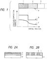
- Symbol "a” of Fig. 1 illustrates schematically the porous regions having different structures or compositions of a semiconductor device of the present invention.
- the semiconductor device of the present invention comprises at least two porous regions 1, 2, 3, etc. having different structures or different compositions.
- the region 2 is the porous region having a fine structure of a composition which performs the intended function of the device
- the region 1 has a structure or a composition which gives a sufficient structural strength. Thereby, the region 1 supports the region 2 to supplement the insufficient structural strength of the region 2 and to make the element practicably stable.
- the region 2 is the porous region having a fine structure or a composition which performs the intended function of the device and the region 1 is a porous region having a different function or characteristics from the region 2, then the device has the both functions or properties of the regions 1 and 2 without impairing the main function of the region 2.
- Symbols "b” and “c” of Fig. 1 show the difference between the regions 1 and 2 in terms of spatial change of parameters of the structure or composition. This change may be abrupt and discontinuous as shown in symbol “b” or otherwise may be gradual and continuous as shown in symbol “c". In the former case, the characteristics at the interface between the regions may be utilized as the function of the element. In the latter case, disadvantages caused by non-conformity between the regions may be reduced.
- the region 3 and following regions including the region 3 may be a porous region which has a structure or composition different from that of the region 1 or 2, or the same structure or composition as that of the region 1 or 2. Otherwise, the region 3 and following regions may be not of the porous structure and may be a constituting region having high structural strength or having excellent signal-energy transmission ability with exterior.
- Figs. 2A and 2B are schematic cross-sectional diagrams of a semiconductor device, showing more specifically embodiment of the aforementioned concept of the element construction.
- Fig. 2A is a cross-sectional view of an example in which the porous regions having different structures or compositions are formed on a substrate in layers parallel to the substrate surface.
- Fig. 2B is a cross-sectional view of another example which has different porous regions partially on the substrate.
- the porous regions are formed on a non-porous substrate 0 and are constructed from a porous regions 1 and 2 having a structure or composition different from each other.
- porous region 1 is the active area which has a brittle structure of structure strength and the porous region 2 has a strong structure, then the stability in structure of the entire element is achievable by either one method of Figs. 2A and 2B.
- the transmission can be practiced through the porous region 2 to the porous region 1 if the porous region 2 is capable of satisfactory transmission.
- FIGs. 2A and 2B illustrate the case where two kinds of porous regions are involved. Naturally, additional different porous regions may coexist.
- the spatial structure of the formed porous material depends largely on the structure and composition of the non-porous material or the working conditions.
- the remaining structure of the porous silicon varies from several ⁇ m to several nm and the network structure of the porous matter varies greatly depending on the kind and the concentration of impurity in the crystalline silicon, the composition and concentration of the anodization solution, the electric current density of the anodization, and so forth.
- a region 4 having different structure or composition is formed preliminarily on a non-porous substrate material 0 as shown in Figs. 3A and 3B. This is conducted by local ion implantation or the like method to modify locally the substrate.
- the substrate is subjected to working 5 from the surface of the substrate 0 for making the substrate porous (Figs. 3C and 3D), the working for porosity including the aforementioned anodization.
- the regions having different structure or composition turn into porous regions 1 and 2 different in the structure or composition from each other even under the same conditions of working for porosity (Figs. 3E and 3F).
- An element having a plurality of porous regions is produced in such a manner.
- a plurality of different kinds of porous regions can be formed by forming the regions by changing the working conditions for porous structure formation.
- Non-porous material 0 having a uniform composition is employed (Figs. 4A and 4B).
- the non-porous material is made porous by working under a certain conditions A to form a porous region 2 (Figs. 4C and 4D).
- a protection measure has to be taken not to make porous the region other than the porous region 2. Specifically, patterning of a protection film, or a like measure is useful. Subsequently, the material is subjected to further porous structure formation working 7 under conditions B different from the conditions A (Figs. 4E and 4F).
- a further porous region 1 is formed additionally inside the porous region 2 with the porous region 2 kept unchanged.
- a porous region 1 is formed in the region other than the porous region 2 if the porous region 2 is protected. If the porous region 1 may be formed directly below the porous region 2 in the construction (Fig. 4F), the protection of the region is not necessary.
- the change of the working conditions leads to a change at least in the structure or, in some cases, in the composition, of the formed porous material, thereby enabling to give different structures or compositions of the porous regions 1 and 2.
- the change of the structure or composition between the different porous regions may be selected readily to be discontinuous and abrupt, or continuous and gradual by controlling the spatial change of the preliminarily formed different structures or compositions, or controlling the time and spatial change of working conditions.
- a light-emitting element employing a porous silicon having an element structure of Fig. 2A was produced by the process shown in Figs. 3A to 3F.
- a monocrystalline silicon wafer of plane orientation [100] doped with boron having resistivity of 0.2 ⁇ cm was used as the substrate and starting non-porous material. This wafer was oxidized by thermal oxidation to form SiO2 layer of about 20 nm thick. Then phosphorus ions accelerated to 25 keV were implanted to the front face of the wafer at a dose of 7 x 1013 cm ⁇ 2 by an ion implantation method. To the back face of the wafer, boron ions accelerated to 40 keV were implanted at a dose of 4 x 1014 cm ⁇ 2. The implanted ions were activated by rapid thermal annealing in a nitrogen atmosphere at 1050°C for one minute.
- the SiO2 layer was removed by using aqueous dilute hydrofluoric acid solution.
- the wafer was immersed in an aqueous 20 wt% hydrofluoric acid/ethanol solution between a pair of parallel plate platinum electrodes such that the portion other than the faces of the wafer was insulated.
- the electrode confronting the wafer front face was employed as the anode, and the wafer was anodized for 2 minutes by applying DC voltage between the platinum electrodes by controlling the current density constant at the wafer face at 10 mA ⁇ cm ⁇ 2.
- the surface of the resulting anodized silicon wafer was maintained in a mirror-polished state without formation of a crack or other defect, but the surface was observed to have discolored owing to the formation of porosity.
- the porosity formation was confirmed by observing a cross-section of a separately prepared sample with a high-resolution electron microscope.
- the anodization proceeded to the depth of about 3 ⁇ m from the surface of the wafer to form a porous layer.
- the outermost thin layer of about 0.1 ⁇ m thick had a coarse structure of several hundred nanometers or more, while most part of the region between the above-mentioned outermost thin layer and the interface with the non-porous portion of the silicon substrate contains a superfine structure of as small as several nanometers.
- the thin coarse-structure layer in the vicinity of the surface is considered to correspond the surface layer which had become n-type by phosphorus ion implantation and annealing for activation practiced prior to the anodization.
- a wafer which was anodized without ion implantation at the surface had a uniform porous layer of a superfine structure and was brittle, so that the porous layer cracked soon after the anodization, or collapsed by slight touching.
- an ITO film of 150 nm thick was formed on the surface of the wafer.
- the ITO film was patterned into several islands of 2 mm square.
- a lead-out electrode was provided by usual wiring technique of the IC process.
- aluminum film of 400 nm thick was formed as the lower electrode.
- the thin coarse n-type porous layer on the front side of the wafer prevents collapse of the directly under superfine porous layer, and simultaneously functions as high efficient current-injecting layer for injecting current into the superfine porous layer on application voltage to the element.
- the element structure having a plurality of porous regions play simultaneously two roles of maintaining both the function and structural strength and of performing a plurality of functions.
- a gas sensor element employing a porous silicon having a structure of Fig. 2B was produced by the process shown in Figs. 4B, 4D and 4F.
- photoresist was applied, and the applied photoresist was patterned by conventional lithography to leave resist pattern of 5 ⁇ m wide on 10 ⁇ m-square lattice lines.
- boron ions accelerated to 50 keV were implanted at a dose of 5 x 1014 cm ⁇ 2.
- the resist was peeled off, and the wafer was subjected to annealing for activation in a nitrogen atmosphere at 950°C for 30 minutes.
- the SiO2 layer was removed by use of dilute hydrofluoric acid aqueous solution.
- the wafer was anodized in the same manner as in Example 1 except for the hydrofluoric acid concentration of 25 %, the current density of 5 mA ⁇ cm ⁇ 2, and the anodization time of 10 minutes.
- the cross-section of the wafer was observed by high-resolution electron microscopy.
- the porous layer had an average thickness of about 2.5 ⁇ m
- the interface between the porous layer and the substrate silicon was not flat and projections and hollows were repeated gently at a cycle of about 10 ⁇ m
- the remaining structure of the porous layer changed from a coarse structure to a superfine structure continuously and synchronously with the projections and hollows.
- the periodical structure is assumed to be due to the two-dimensional distribution of the resistivity caused by local boron ion implantation at the back face of the wafer, and the corresponding spatial modulation of the electric current in the plane on the anodization.
- the structural strength of the entire porous layer is considered to be achieved by the coarse structure which supports mechanically the interposed superfine porous regions.
- an aluminum electrode was deposited by mask vapor deposition in a thickness of 300 nm on the front face of the wafer, and aluminum film was formed in a thickness of 400 nm over the entire of the back face by sputtering.
- the dependence of electric characteristics on the atmosphere around the element was investigated with the element formed between the electrodes on the both faces of the wafer prepared in this Example.
- the electric capacity of the element was measured by varying the amount of vapor of water or alcohol in the air. In the both cases, the electric capacity of the element increased gradually with the amount of vapor with saturation tendency, which shows the function of the element as a gas sensor.
- a light-emitting element employing a porous silicon having an element structure of Fig. 2A was produced by the process shown in Fig. 4A, 4C and 4E.
- a monocrystalline silicon wafer of plane orientation [111] doped with boron having resistivity of 1 ⁇ cm was used as the substrate and starting non-porous material.
- an aluminum film of 400 nm thick was formed, and annealed in a hydrogen atmosphere at 400°C for 30 minutes.
- the surface of the wafer was immersed in aqueous hydrofluoric acid/ethanol solution the wafer was anodized by using the aluminum film of the back face as the cathode and an opposing platinum electrode as the anode.
- the hydrofluoric acid concentration of the etching solution was 35 %, and the current density and the anodization time were varied successively in seven steps as shown in the Table below.
- the surface of the resulting anodized silicon surface was kept in a mirror-polished state without formation of a crack or other defect, but the surface was observed to have discolored owing to the formation of porosity.
- the cross-section of the sample was observed.
- the outermost surface layer of about 10 ⁇ m in a total thickness had a coarse structure and the under portion had a superfine porous structure.
- the superfine porous layer was composed of six layers, and the respective layers had slightly different structure from each other although the differences were not so significant as the difference between the outermost layer and the inner layer. Naturally, the differences of the structure among the layers are caused by the change of the electric current density during the each porous layer formation.
- the spectrum of the light emitted by the element showed that the light had a relatively flat emission strength over the range of from 500 nm to 800 nip or more. If the superfine porous silicon layer is formed under fixed conditions, the light emission spectra will distribute broadly and have a peak which tends to shift shorter wavelength corresponding to finer porous structure. Therefore, the white light emitted by the light-emitting element of this Example is considered to be due to the appropriate superposition of emission spectra of a plurality of porous layers having different size of structures.
- the porous layer of the coarse structure at the outermost layer supports mechanically the layer of the under portion having a brittle superfine structure to achieve structural stability of the element.
- a light-emitting element was prepared by employing porous silicon and silicon-germanium.
- boron ions accelerated to 40 kev was implanted at a dose of 4 X 1014 cm ⁇ 2, and subjected to annealing for activation in an nitrogen atmosphere at 1000°C for 10 minutes.
- a multi-layered film having a quantum well structure of Si/SiGe was formed by low pressure CVD as follows. Firstly, a Si 0.95 Ge 0.05 buffer layer of 300 nm thick was formed on the wafer. Then, formation of an Si 0.8 Ge 0.2 layer of 5 nm thick and subsequent formation of an Si layer of 20 nm thick were repeated 20 times. Finally a boron-doped Si layer of 150 nm thick was formed thereon.
- an aluminum film of 400 nm thick was formed, and was annealed in a hydrogen atmosphere at 400°C for 30 minutes.
- Example 3 Anodization was conducted in the same manner as in Example 3 except that the hydrofluoric acid of the etching solution was 45 %, the electric current density was 20 mA ⁇ cm ⁇ 2, and the anodization time was 2 minutes.
- the surface of the resulting anodized silicon wafer surface was kept in a mirror-polished state without formation of a crack or other defect, but the surface was observed to have discolored owing to the formation of porosity.
- the cross-section of a separately prepared sample was observed with a transmission type electron microscope, and found that the porous layer had a total thickness of about 1.5 ⁇ m and the portion of the porous layer of from the surface to a depth of about 150 nm had a coarse structure. This coarse structure is considered to be formed from high-concentration boron-doped Si layer by porous structure formation.
- the multilayer region of Si/SiGe quantum well immediately below the coarse portion are equally of a superfine structure, and the difference of the structure caused by the difference of the composition was not detected because of the extreme thinness of the respective layers.
- the superfine structure portion is considered to be supported by the coarse structure layer on the surface without spontaneous collapse.
- an aluminum electrode was formed in a shape of a comb on the front face of the wafer.
- the porous layer of the coarse structure at the outermost layer supports mechanically the layer at the under portion having a brittle superfine structure to achieve structural stability of the element.
- a light-emitting element was prepared by employing porous silicon and gallium-aluminum-arsine.
- a monocrystalline silicon substrate of plane orientation [100] doped with boron having resistivity of 10 ⁇ cm was prepared.
- boron ions accelerated to 50 keV were implanted at a dose of 5 X 1014 cm ⁇ 2 and activated by thermal annealing in a nitrogen atmosphere at 950°C for 30 minutes.
- a gallium-aluminum-arsine layer of 1 ⁇ m thick was formed by an MBE process, and further thereon a silicon layer doped with high concentration of arsine was epitaxially grown to a thickness of 200 nm by bias sputtering to obtain a supporting substrate and non-porous starting material.
- Example 2 Anodization was conducted in the same manner as in Example 1 except that the concentration of the hydrofluoric acid in the etching solution was 25 %, the current density was 10 mA ⁇ cm ⁇ 2, and the anodization time was 10 minutes.
- the surface of the resulting anodized silicon wafer was kept in a mirror-polished state without formation of a crack or other defect, but the surface was observed to have discolored owing to the formation of porosity.
- the cross-section of the sample was observed by electron microscopy, and found that a multi-layer structure was formed in which the outermost silicon layer had a coarse structure, the directly under gallium-aluminum-arsine layer had a superfine structure, and the region anodized to the silicon substrate had a superfine structure. At least, the outermost layer of the coarse structure surely gave additional structural strength to the superfine porous layer to stabilize it.
- the electrode was formed in the same manner as in Example 1.
- the semiconductor device of the present invention has a plurality of porous regions having different structures or compositions: some porous region has fine structure performing the main function of the device, and another porous region has a coarse structure having sufficient strength to support the fine porous region structurally.
- a semiconductor device which employs porous functional material having practicably sufficient strength without impairing the intended function.
- the process of the present invention produces a semiconductor device having a plurality of porous regions having different structures or compositions readily with sufficient controlability by modifying partially a non-porous material and subsequently making the material porous, or by changing the treating conditions for porous structure formation, or by a like method.
- a semiconductor device having a porous member as an active region, the porous member comprising a plurality of porous regions having different structures or compositions; and a process for producing a semiconductor device, comprising a step of modifying partially a non-porous substrate, and a subsequent step of making the substrate porous.
Abstract
Description
- The present invention relates to a semiconductor device such as an electronic element, an optical element, and integrated circuit thereof which performs functions of light-emission, sensing, or the like, and also relates to a process for producing the semiconductor device. In particular, the present invention relates to a semiconductor device having a porous region and to a process for producing the device.
- Porous materials are attracting attention in recent years as a novel functional material for constituting an active region of an element.
- The porous structure of semiconductor crystal of Group IV, for example, were mainly used in the past as structural members which are not related to the electronic and optical properties of the material: the uses such as formation of SOI (Silicon On Insulator) structure utilizing capability of high speed oxidation (see, for example, T. Unagami and M. Seki: J. Electrochem. Soc., 125, 1339 (1978)).
- In recent years, the porous material is applied to an active region material of a gas sensor by utilizing the large surface area resulting from the porosity (see, for example, A. Motohashi, et al.: Oyo Butsuri Gakkai Gakujutsu Koenkai (Shuki) Yokoshu (Preprint of Autumnal Meeting of Society of Applied Physics), 29p-ZB-9 (1986)); and light-emission phenomenon was discovered which is caused by a structure sufficiently fine for imprisonment of carrier quantum (see L.T. Canham, Appl. Phys. Lett., 56, 1046 (1990)). Since then, studies are being made actively on functional application of porous material to light-emitting element, and other applications. The functional application of the porous material will possibly become an attractive novel technique if several practical problems are solved, because the porous structure can be formed readily by treating the base material.
- The most serious of the problems in realization of the functional application of the porous material is the lack of stability of structure of the material.
- The porous material, as understood from the name, has many voids in the space where the material is to be filled inherently. Therefore, the structural strength is unavoidably low in comparison with the base material. Further the absolute value of the strength naturally depends on the size, shape, density, and so forth of the remaining structure. A material of finer porous structure is generally more brittle than the one having a coarser structure. Accordingly, a coarse porous material is advantageous as far as desired functions are performed with the coarse structure. However, in application fields in which finer structure is required, the structural instability becomes a serious problem.
- Referring again to the example of the aforementioned semiconductor crystal of Group IV, a finer structure is desired to obtain a larger surface area for higher sensitivity of a gas sensor; and visible light-emission is not achievable without a superfine structure of finer than several nanometers. In the latter application, to obtain shorter wavelength of emitted light, much more finer structure is required.
- Practically, however, such a superfine porous material is extremely brittle, and will collapse immediately on touching. Therefore, it is extremely difficult to practicalize the instable material with a definite element size.
- Another problem in functional application of a porous material is the difficulty of signal transmission between the porous active region and the outside.
- The active element needs to transmit or receive signal or energy to or from the porous region. However, the porous structure or the composition of the intended porous material is frequently not suitable for the transmittance function. For example, the aforementioned light-emitting element involves the problem that an electrode formed for injecting carriers into the porous active region is insufficient in structural strength and further does not give sufficient injection efficiency because of excessively high contact resistance.
- Generally, unsolved problems exist not only in transmission of signals and energies but also in simultaneous practice of a plurality of functions.
- An object of the present invention is not only to improve a structural strength of a semiconductor device having fine porous regions but also to provide a semiconductor device having fine porous regions which is improved in signal-energy transmission ability of the fine porous regions.
- Another object of the present invention is to provide a semiconductor device which performs a plurality of functions which cannot be achieved by a device having only one kind of porous regions and to provide a process for producing the device.
- Fig. 1 is a schematic diagram showing an embodiment of a semiconductor device having a plurality of different porous regions of the present invention.
- Figs. 2A and 2B illustrate schematic sectional views showing an embodiment of element construction of a semiconductor device of the present invention.
- Figs. 3A to 3F illustrate sectional views showing an embodiment of the process for producing a semiconductor device of the present invention.
- Figs. 4A to 4F illustrate sectional views showing an embodiment of the process for producing a semiconductor device of the present invention.
- The semiconductor device having a porous member as an active region of the present invention comprises a plurality of porous regions having different structures or compositions.
- In one embodiment, the structure or composition changes discontinuously between the plurality of porous regions having different structures or compositions.
- In another embodiment, the structure or composition changes continuously between the plurality of porous regions having different structures or compositions.
- In still another embodiment, a porous region having a fine structure is supported by a porous region having a coarse structure.
- The process for producing the semiconductor of the present invention comprises modifying partially a non-porous substrate, then making the substrate porous.
- The another process for producing the semiconductor of the present invention comprises making a non-porous substrate porous by changing working conditions of porous structure formation.
- The semiconductor device of the present invention has a plurality of porous regions having different structures or compositions. Some active regions may have a fine porous structure and perform a function of the main purpose, while other regions may have a coarse structure which has sufficient strength to support the aforementioned fine porous region structurally. Thereby the semiconductor device serves as a practically useful porous material without impairing the intended function.
- Regions other than the main fine porous regions may be porous regions which have a structure and a composition showing a function and characteristics different from the main fine porous regions. Thereby a semiconductor device is provided which has porous active elements having multiple functions without impairing the main object.
- In the process for producing a semiconductor device of the present invention, a non-porous material is made porous by utilizing a material difference of the non-porous material or by changing the working conditions. Thereby a semiconductor device is producible practicably which has a plurality of porous regions having different structures or compositions.
- The embodiment of the semiconductor device and the process for producing it are described below in detail by reference to drawings.
- Symbol "a" of Fig. 1 illustrates schematically the porous regions having different structures or compositions of a semiconductor device of the present invention. In symbol "a" of Fig. 1, the semiconductor device of the present invention comprises at least two
porous regions - If the
region 2 is the porous region having a fine structure of a composition which performs the intended function of the device, theregion 1 has a structure or a composition which gives a sufficient structural strength. Thereby, theregion 1 supports theregion 2 to supplement the insufficient structural strength of theregion 2 and to make the element practicably stable. If theregion 2 is the porous region having a fine structure or a composition which performs the intended function of the device and theregion 1 is a porous region having a different function or characteristics from theregion 2, then the device has the both functions or properties of theregions region 2. - Symbols "b" and "c" of Fig. 1 show the difference between the
regions - The
region 3 and following regions including theregion 3 may be a porous region which has a structure or composition different from that of theregion region region 3 and following regions may be not of the porous structure and may be a constituting region having high structural strength or having excellent signal-energy transmission ability with exterior. - Figs. 2A and 2B are schematic cross-sectional diagrams of a semiconductor device, showing more specifically embodiment of the aforementioned concept of the element construction. Fig. 2A is a cross-sectional view of an example in which the porous regions having different structures or compositions are formed on a substrate in layers parallel to the substrate surface. Fig. 2B is a cross-sectional view of another example which has different porous regions partially on the substrate.
- In Figs. 2A and 2B, the porous regions are formed on a
non-porous substrate 0 and are constructed from aporous regions - If the
porous region 1 is the active area which has a brittle structure of structure strength and theporous region 2 has a strong structure, then the stability in structure of the entire element is achievable by either one method of Figs. 2A and 2B. - Even when direct transmission of signal or energy to the
porous region 2 is difficult, the transmission can be practiced through theporous region 2 to theporous region 1 if theporous region 2 is capable of satisfactory transmission. - Figs. 2A and 2B illustrate the case where two kinds of porous regions are involved. Naturally, additional different porous regions may coexist.
- The formation of a plurality of porous regions according to the process for producing a semiconductor device according to the present invention is described regarding the element construction shown in Figs. 2A and 2B.
- Generally, in making a non-porous material porous by working such as etching, the spatial structure of the formed porous material depends largely on the structure and composition of the non-porous material or the working conditions. For example, in formation of porous silicon by anodization of crystalline silicon, the remaining structure of the porous silicon varies from several µm to several nm and the network structure of the porous matter varies greatly depending on the kind and the concentration of impurity in the crystalline silicon, the composition and concentration of the anodization solution, the electric current density of the anodization, and so forth.
- A
region 4 having different structure or composition is formed preliminarily on anon-porous substrate material 0 as shown in Figs. 3A and 3B. This is conducted by local ion implantation or the like method to modify locally the substrate. - Subsequently, the substrate is subjected to working 5 from the surface of the
substrate 0 for making the substrate porous (Figs. 3C and 3D), the working for porosity including the aforementioned anodization. The regions having different structure or composition turn intoporous regions - A plurality of different kinds of porous regions can be formed by forming the regions by changing the working conditions for porous structure formation.
- A process for realizing the element structures of Figs. 2A and 2B is illustrated in Figs. 4A to 4F.
Non-porous material 0 having a uniform composition is employed (Figs. 4A and 4B). The non-porous material is made porous by working under a certain conditions A to form a porous region 2 (Figs. 4C and 4D). To make the construction of Figs. 4B, 4D and 4F, a protection measure has to be taken not to make porous the region other than theporous region 2. Specifically, patterning of a protection film, or a like measure is useful. Subsequently, the material is subjected to further porous structure formation working 7 under conditions B different from the conditions A (Figs. 4E and 4F). Thereby, in the element construction (Fig. 4E), a furtherporous region 1 is formed additionally inside theporous region 2 with theporous region 2 kept unchanged. On the other hand, in element construction (Fig. 4F), aporous region 1 is formed in the region other than theporous region 2 if theporous region 2 is protected. If theporous region 1 may be formed directly below theporous region 2 in the construction (Fig. 4F), the protection of the region is not necessary. - In the case where a spatial modulation of working conditions is possible, the aforementioned protection and two-step working is not required, and steps of Figs. 4D and 4F may be conducted simultaneously.
- The change of the working conditions leads to a change at least in the structure or, in some cases, in the composition, of the formed porous material, thereby enabling to give different structures or compositions of the
porous regions - The processes for producing a semiconductor device of the present invention are described above by reference to Figs. 3A to 3F and Figs. 4A to 4F, in which the composition of the starting material for the porous material or the working conditions are changed respectively. Both methods may naturally be combinedly employed.
- The above description is made regarding the production of elements having two kinds of porous regions. It is evident naturally that more than two kinds of layers of element structure can be formed in a similar process.
- Further, the change of the structure or composition between the different porous regions may be selected readily to be discontinuous and abrupt, or continuous and gradual by controlling the spatial change of the preliminarily formed different structures or compositions, or controlling the time and spatial change of working conditions.
- The construction of the element of the semiconductor device and the process for production thereof of the present invention are described more specifically by reference to typical examples.
- A light-emitting element employing a porous silicon having an element structure of Fig. 2A was produced by the process shown in Figs. 3A to 3F.
- A monocrystalline silicon wafer of plane orientation [100] doped with boron having resistivity of 0.2 Ω·cm was used as the substrate and starting non-porous material. This wafer was oxidized by thermal oxidation to form SiO₂ layer of about 20 nm thick. Then phosphorus ions accelerated to 25 keV were implanted to the front face of the wafer at a dose of 7 x 10¹³ cm⁻² by an ion implantation method. To the back face of the wafer, boron ions accelerated to 40 keV were implanted at a dose of 4 x 10¹⁴ cm⁻². The implanted ions were activated by rapid thermal annealing in a nitrogen atmosphere at 1050°C for one minute. Thereafter the SiO₂ layer was removed by using aqueous dilute hydrofluoric acid solution. The wafer was immersed in an aqueous 20 wt% hydrofluoric acid/ethanol solution between a pair of parallel plate platinum electrodes such that the portion other than the faces of the wafer was insulated. The electrode confronting the wafer front face was employed as the anode, and the wafer was anodized for 2 minutes by applying DC voltage between the platinum electrodes by controlling the current density constant at the wafer face at 10 mA·cm⁻².
- The surface of the resulting anodized silicon wafer was maintained in a mirror-polished state without formation of a crack or other defect, but the surface was observed to have discolored owing to the formation of porosity. The porosity formation was confirmed by observing a cross-section of a separately prepared sample with a high-resolution electron microscope. The anodization proceeded to the depth of about 3 µm from the surface of the wafer to form a porous layer. By more careful observation, the outermost thin layer of about 0.1 µm thick had a coarse structure of several hundred nanometers or more, while most part of the region between the above-mentioned outermost thin layer and the interface with the non-porous portion of the silicon substrate contains a superfine structure of as small as several nanometers. The thin coarse-structure layer in the vicinity of the surface is considered to correspond the surface layer which had become n-type by phosphorus ion implantation and annealing for activation practiced prior to the anodization. On the other hand, a wafer which was anodized without ion implantation at the surface had a uniform porous layer of a superfine structure and was brittle, so that the porous layer cracked soon after the anodization, or collapsed by slight touching.
- After confirmation of sufficient stability of the porous layer of the wafer having been subjected to phosphorus ion implantation and anodization, an ITO film of 150 nm thick was formed on the surface of the wafer. The ITO film was patterned into several islands of 2 mm square. To each of the islands of ITO film, a lead-out electrode was provided by usual wiring technique of the IC process. Over the entire of the back face of the wafer, aluminum film of 400 nm thick was formed as the lower electrode.
- With the element prepared above, DC current was made to flow between the electrodes on the both faces of the wafer. The element exhibited rectification characteristics to flow electric current with the back face electrodes employed as the anode, and emitted visible orange light with the threshold voltage of about 5 V. This light emission is considered to be due to electroluminescence caused by current injection into the superfine porous silicon layer through the junction interface between the coarse n-type porous layer and directly under p-type porous layer.
- In this Example, of the two porous layer having different structure/composition, the thin coarse n-type porous layer on the front side of the wafer, with its structural strength, prevents collapse of the directly under superfine porous layer, and simultaneously functions as high efficient current-injecting layer for injecting current into the superfine porous layer on application voltage to the element. Thus the element structure having a plurality of porous regions play simultaneously two roles of maintaining both the function and structural strength and of performing a plurality of functions.
- A gas sensor element employing a porous silicon having a structure of Fig. 2B was produced by the process shown in Figs. 4B, 4D and 4F.
- A monocrystalline silicon wafer of plane orientation [110] doped with boron having resistivity of 10 Ω·cm, and having been polished on both sides was used as the substrate and starting non-porous material. This wafer was oxidized by thermal oxidation to form SiO₂ layer of about 30 nm thick. On the back face of the wafer, photoresist was applied, and the applied photoresist was patterned by conventional lithography to leave resist pattern of 5 µm wide on 10 µm-square lattice lines. To the back face of the wafer, boron ions accelerated to 50 keV were implanted at a dose of 5 x 10¹⁴ cm⁻². The resist was peeled off, and the wafer was subjected to annealing for activation in a nitrogen atmosphere at 950°C for 30 minutes. Then the SiO₂ layer was removed by use of dilute hydrofluoric acid aqueous solution.
- The wafer was anodized in the same manner as in Example 1 except for the hydrofluoric acid concentration of 25 %, the current density of 5 mA·cm⁻², and the anodization time of 10 minutes.
- In the wafer having been subjected to local ion injection like the one of this Example, the three-dimensional structure seemed to be maintained at least although significant change of color of the surface is exhibited and the surface is not in a mirror-polished state.
- The cross-section of the wafer was observed by high-resolution electron microscopy. As the results, it was found that the porous layer had an average thickness of about 2.5 µm, the interface between the porous layer and the substrate silicon was not flat and projections and hollows were repeated gently at a cycle of about 10 µm, and the remaining structure of the porous layer changed from a coarse structure to a superfine structure continuously and synchronously with the projections and hollows. The periodical structure is assumed to be due to the two-dimensional distribution of the resistivity caused by local boron ion implantation at the back face of the wafer, and the corresponding spatial modulation of the electric current in the plane on the anodization. The structural strength of the entire porous layer is considered to be achieved by the coarse structure which supports mechanically the interposed superfine porous regions.
- For comparison, a wafer was prepared which was implanted with ions uniformly on the back face without using resist pattern. This wafer began to collapse spontaneously at the porous surface immediately after washing and drying of the wafer, and the electron microscopical observation was not feasible.
- Finally, after confirming the sufficient stability of the porous layer of the wafer surface, an aluminum electrode was deposited by mask vapor deposition in a thickness of 300 nm on the front face of the wafer, and aluminum film was formed in a thickness of 400 nm over the entire of the back face by sputtering.
- The dependence of electric characteristics on the atmosphere around the element was investigated with the element formed between the electrodes on the both faces of the wafer prepared in this Example. The electric capacity of the element was measured by varying the amount of vapor of water or alcohol in the air. In the both cases, the electric capacity of the element increased gradually with the amount of vapor with saturation tendency, which shows the function of the element as a gas sensor.
- A light-emitting element employing a porous silicon having an element structure of Fig. 2A was produced by the process shown in Fig. 4A, 4C and 4E.
- A monocrystalline silicon wafer of plane orientation [111] doped with boron having resistivity of 1 Ω·cm was used as the substrate and starting non-porous material. On the entire of the back face of the wafer, an aluminum film of 400 nm thick was formed, and annealed in a hydrogen atmosphere at 400°C for 30 minutes. Then only the surface of the wafer was immersed in aqueous hydrofluoric acid/ethanol solution the wafer was anodized by using the aluminum film of the back face as the cathode and an opposing platinum electrode as the anode. The hydrofluoric acid concentration of the etching solution was 35 %, and the current density and the anodization time were varied successively in seven steps as shown in the Table below.
Table 1 Step Current density (mA·cm⁻²) Anodization time (minutes) 1 0.5 20 2 5 4 3 10 2 4 5 4 5 15 1.5 6 5 4 7 20 1 - The surface of the resulting anodized silicon surface was kept in a mirror-polished state without formation of a crack or other defect, but the surface was observed to have discolored owing to the formation of porosity. The cross-section of the sample was observed. As the results, the outermost surface layer of about 10 µm in a total thickness had a coarse structure and the under portion had a superfine porous structure. According to more careful observation, the superfine porous layer was composed of six layers, and the respective layers had slightly different structure from each other although the differences were not so significant as the difference between the outermost layer and the inner layer. Naturally, the differences of the structure among the layers are caused by the change of the electric current density during the each porous layer formation.
- After confirmation of the sufficient stability of the porous layer of the wafer surface, a thin gold film of 20 nm thick was deposited on the wafer surface by mask vapor-deposition.
- With the element prepared above, DC current was made to flow between the electrodes on the front and back faces of the wafer. The element exhibited rectification characteristics to flow electric current with the electrode on the back side employed as the anode, and emitted slightly warm-colored white visible light with the threshold voltage of about 10 V. This light emission is considered to be due to electroluminescence caused by current injection through the interface of gold of Schottky type junction into the superfine porous silicon layer.
- The spectrum of the light emitted by the element showed that the light had a relatively flat emission strength over the range of from 500 nm to 800 nip or more. If the superfine porous silicon layer is formed under fixed conditions, the light emission spectra will distribute broadly and have a peak which tends to shift shorter wavelength corresponding to finer porous structure. Therefore, the white light emitted by the light-emitting element of this Example is considered to be due to the appropriate superposition of emission spectra of a plurality of porous layers having different size of structures.
- As above, a plurality of the porous layers of the element coexist to perform a plurality of functions without impairing the functions of the respective layers, thereby achieving the second object of the present invention. Further, the first object of the present invention is simultaneously achieved in that the porous layer of the coarse structure at the outermost layer supports mechanically the layer of the under portion having a brittle superfine structure to achieve structural stability of the element.
- A light-emitting element was prepared by employing porous silicon and silicon-germanium. A monocrystalline silicon wafer of plane orientation [100] doped with boron having resistivity of 10 Ω·cm. To the back face of the wafer, boron ions accelerated to 40 kev was implanted at a dose of 4 X 10¹⁴ cm⁻², and subjected to annealing for activation in an nitrogen atmosphere at 1000°C for 10 minutes.
- On the front face of the wafer, a multi-layered film having a quantum well structure of Si/SiGe was formed by low pressure CVD as follows. Firstly, a Si0.95Ge0.05 buffer layer of 300 nm thick was formed on the wafer. Then, formation of an Si0.8Ge0.2 layer of 5 nm thick and subsequent formation of an Si layer of 20 nm thick were repeated 20 times. Finally a boron-doped Si layer of 150 nm thick was formed thereon.
- Over the entire of the back face, an aluminum film of 400 nm thick was formed, and was annealed in a hydrogen atmosphere at 400°C for 30 minutes.
- Subsequently, anodization was conducted in the same manner as in Example 3 except that the hydrofluoric acid of the etching solution was 45 %, the electric current density was 20 mA·cm⁻², and the anodization time was 2 minutes.
- The surface of the resulting anodized silicon wafer surface was kept in a mirror-polished state without formation of a crack or other defect, but the surface was observed to have discolored owing to the formation of porosity. The cross-section of a separately prepared sample was observed with a transmission type electron microscope, and found that the porous layer had a total thickness of about 1.5 µm and the portion of the porous layer of from the surface to a depth of about 150 nm had a coarse structure. This coarse structure is considered to be formed from high-concentration boron-doped Si layer by porous structure formation. The multilayer region of Si/SiGe quantum well immediately below the coarse portion are equally of a superfine structure, and the difference of the structure caused by the difference of the composition was not detected because of the extreme thinness of the respective layers. The superfine structure portion is considered to be supported by the coarse structure layer on the surface without spontaneous collapse.
- Then, an aluminum electrode was formed in a shape of a comb on the front face of the wafer.
- With the element prepared above, DC current was made to flow between the electrode on the front and back faces of the wafer, whereby visible light was emitted at a room temperature in the current direction where the electrode on the front face was used as the anode. The spectrum of the emitted light had a distinct peak at about 650 nm, and the emitted light was highly monochromatic. This is presumably due to the fact below. The superfine porous structure was given to the two-dimensional quantum well structure of the original multi-layered film prior to porous structure formation, whereby a three-dimensional quantum well structure having relatively uniform enclosure size. Consequently, in a non-porous multilayered film, the wavelength of the peak of the emitted light which was at the longer wavelength side than the more highly monochromatic light shifted to the shorter wavelength side, while in the porous film of Si or SiGe which is not of a multi-layered structure, the broad spectrum of the visible light emitted at a room temperature became sharp.
- In such a manner, a plurality of the porous layers of the element coexist to perform a plurality of functions without impairing the functions of the respective layers, thereby achieving the second object of the present invention. Further, the first object of the present invention is simultaneously achieved in that the porous layer of the coarse structure at the outermost layer supports mechanically the layer at the under portion having a brittle superfine structure to achieve structural stability of the element.
- A light-emitting element was prepared by employing porous silicon and gallium-aluminum-arsine.
- A monocrystalline silicon substrate of plane orientation [100] doped with boron having resistivity of 10 Ω·cm was prepared. To the back face of the substrate, boron ions accelerated to 50 keV were implanted at a dose of 5 X 10¹⁴ cm⁻² and activated by thermal annealing in a nitrogen atmosphere at 950°C for 30 minutes. On the front face of the wafer, a gallium-aluminum-arsine layer of 1 µm thick was formed by an MBE process, and further thereon a silicon layer doped with high concentration of arsine was epitaxially grown to a thickness of 200 nm by bias sputtering to obtain a supporting substrate and non-porous starting material.
- Then anodization was conducted in the same manner as in Example 1 except that the concentration of the hydrofluoric acid in the etching solution was 25 %, the current density was 10 mA·cm⁻², and the anodization time was 10 minutes.
- The surface of the resulting anodized silicon wafer was kept in a mirror-polished state without formation of a crack or other defect, but the surface was observed to have discolored owing to the formation of porosity. The cross-section of the sample was observed by electron microscopy, and found that a multi-layer structure was formed in which the outermost silicon layer had a coarse structure, the directly under gallium-aluminum-arsine layer had a superfine structure, and the region anodized to the silicon substrate had a superfine structure. At least, the outermost layer of the coarse structure surely gave additional structural strength to the superfine porous layer to stabilize it. Practically, aluminum in the gallium-aluminium-arsine layer is damaged by hydrofluoric acid, and the anodization of gallium-arsine gives only a brittle porous matter. Therefore, a sample which had been anodized without preliminary formation of an outermost silicon layer could not be used for subsequent process such as electrode formation.
- Finally, on each face of the wafer, the electrode was formed in the same manner as in Example 1.
- DC current was made to flow between the electrodes of the element, and the edge face of the lamination structure was observed. Thereby light was found to be emitted from the gallium-aluminum-arsine layer having a superfine porous structure. The intensity of the emitted light was about ten times that of the non-porous gallium-aluminum-arsine, and the peak wavelength shifted by about 100 nm to the high energy side. These results are considered to result from a kind of multiple quantum well structure formed by porous structure formation of a superfine structure of gallium-aluminum-arsine.
- As described above, the semiconductor device of the present invention has a plurality of porous regions having different structures or compositions: some porous region has fine structure performing the main function of the device, and another porous region has a coarse structure having sufficient strength to support the fine porous region structurally. Thereby, a semiconductor device is provided which employs porous functional material having practicably sufficient strength without impairing the intended function.
- The process of the present invention produces a semiconductor device having a plurality of porous regions having different structures or compositions readily with sufficient controlability by modifying partially a non-porous material and subsequently making the material porous, or by changing the treating conditions for porous structure formation, or by a like method.
- Disclosed are a semiconductor device having a porous member as an active region, the porous member comprising a plurality of porous regions having different structures or compositions; and a process for producing a semiconductor device, comprising a step of modifying partially a non-porous substrate, and a subsequent step of making the substrate porous.
Claims (8)
- A semiconductor device having a porous member as an active region, the porous member comprising a plurality of porous regions having different structures or compositions.
- A semiconductor device according to Claim 1, wherein the plurality of porous regions comprises a first porous region having a fine structure and a second porous region having a coarse structure for supporting the first porous region structurally.
- A semiconductor device according to Claim 1, wherein the structure or the composition changes discontinuously between the plurality of porous regions having different structures or compositions.
- A semiconductor device according to Claim 1, wherein the structure or the composition changes continuously between the plurality of porous regions having different structures or compositions.
- A process for producing a semiconductor device, comprising a step of modifying partially a non-porous substrate, and a subsequent step of making the substrate porous.
- A process for producing a semiconductor device according to Claim 5, wherein the step of modifying partially the non-porous substrate is partial ion implantation.
- A process for producing a semiconductor device, comprising a step of making the non-porous substrate porous by changing the working conditions for porous structure formation.
- A process for producing a semiconductor device according to Claim 7, wherein the step of making the non-porous substrate porous is anodization, and the non-porous substrate is made porous by changing current density and anodization time stepwise.
Applications Claiming Priority (3)
| Application Number | Priority Date | Filing Date | Title |
|---|---|---|---|
| JP247175/92 | 1992-08-25 | ||
| JP24717592 | 1992-08-25 | ||
| JP24717592A JP3352118B2 (en) | 1992-08-25 | 1992-08-25 | Semiconductor device and manufacturing method thereof |
Publications (3)
| Publication Number | Publication Date |
|---|---|
| EP0584777A1 true EP0584777A1 (en) | 1994-03-02 |
| EP0584777B1 EP0584777B1 (en) | 2000-11-08 |
| EP0584777B2 EP0584777B2 (en) | 2004-01-02 |
Family
ID=17159558
Family Applications (1)
| Application Number | Title | Priority Date | Filing Date |
|---|---|---|---|
| EP93113472A Expired - Lifetime EP0584777B2 (en) | 1992-08-25 | 1993-08-24 | Semiconductor device and process for producing the same |
Country Status (4)
| Country | Link |
|---|---|
| US (1) | US5970361A (en) |
| EP (1) | EP0584777B2 (en) |
| JP (1) | JP3352118B2 (en) |
| DE (1) | DE69329635T3 (en) |
Cited By (5)
| Publication number | Priority date | Publication date | Assignee | Title |
|---|---|---|---|---|
| EP0767486A2 (en) * | 1995-10-06 | 1997-04-09 | Canon Kabushiki Kaisha | Semiconductor substrate and producing method thereof |
| EP0902486A2 (en) * | 1997-09-11 | 1999-03-17 | Kokusai Denshin Denwa Kabushiki Kaisha | Semiconductor light emitting device and method for manufacturing the same |
| EP0975012A2 (en) * | 1998-07-23 | 2000-01-26 | Canon Kabushiki Kaisha | Porous silicon with uniform pore size distribution |
| WO2002051741A2 (en) * | 2000-12-22 | 2002-07-04 | Robert Bosch Gmbh | Method for producing a semiconductor component having a movable mass in particular, and semiconductor component produced according to this method |
| US7148119B1 (en) | 1994-03-10 | 2006-12-12 | Canon Kabushiki Kaisha | Process for production of semiconductor substrate |
Families Citing this family (41)
| Publication number | Priority date | Publication date | Assignee | Title |
|---|---|---|---|---|
| US6121112A (en) * | 1905-08-29 | 2000-09-19 | Canon Kabushiki Kaisha | Fabrication method for semiconductor substrate |
| US20030087503A1 (en) * | 1994-03-10 | 2003-05-08 | Canon Kabushiki Kaisha | Process for production of semiconductor substrate |
| JP3490903B2 (en) * | 1997-09-11 | 2004-01-26 | Kddi株式会社 | Semiconductor light emitting device and method of manufacturing the same |
| US6197654B1 (en) * | 1998-08-21 | 2001-03-06 | Texas Instruments Incorporated | Lightly positively doped silicon wafer anodization process |
| US6375738B1 (en) | 1999-03-26 | 2002-04-23 | Canon Kabushiki Kaisha | Process of producing semiconductor article |
| FR2797093B1 (en) * | 1999-07-26 | 2001-11-02 | France Telecom | PROCESS FOR PRODUCING A DEVICE INCLUDING A STACK OF QUANTITY BOXES ON A SINGLE-CRYSTAL SILICON OR GERMANIUM SUBSTRATE |
| DE10006528C2 (en) * | 2000-02-15 | 2001-12-06 | Infineon Technologies Ag | Fuse arrangement for a semiconductor device |
| JP2001284622A (en) | 2000-03-31 | 2001-10-12 | Canon Inc | Method for manufacturing semiconductor member and method for manufacturing solar cell |
| US6790785B1 (en) | 2000-09-15 | 2004-09-14 | The Board Of Trustees Of The University Of Illinois | Metal-assisted chemical etch porous silicon formation method |
| WO2002103752A2 (en) | 2000-11-27 | 2002-12-27 | The Board Of Trustees Of The University Of Illinois | Metal-assisted chemical etch to produce porous group iii-v materials |
| FR2823596B1 (en) * | 2001-04-13 | 2004-08-20 | Commissariat Energie Atomique | SUBSTRATE OR DISMOUNTABLE STRUCTURE AND METHOD OF MAKING SAME |
| JP4310076B2 (en) * | 2001-05-31 | 2009-08-05 | キヤノン株式会社 | Method for producing crystalline thin film |
| EP1341222A1 (en) * | 2002-02-28 | 2003-09-03 | Interuniversitair Micro-Elektronica Centrum | A method for producing a device having a semiconductor layer on a lattice mismatched substrate |
| JP2004335642A (en) * | 2003-05-06 | 2004-11-25 | Canon Inc | Substrate and its producing process |
| KR20060017771A (en) * | 2003-05-06 | 2006-02-27 | 캐논 가부시끼가이샤 | Semiconductor substrate, semiconductor device, light emitting diode and producing method therefor |
| US20050124137A1 (en) * | 2003-05-07 | 2005-06-09 | Canon Kabushiki Kaisha | Semiconductor substrate and manufacturing method therefor |
| TWI242232B (en) * | 2003-06-09 | 2005-10-21 | Canon Kk | Semiconductor substrate, semiconductor device, and method of manufacturing the same |
| JP2005005509A (en) * | 2003-06-12 | 2005-01-06 | Canon Inc | Thin film transistor and method of manufacturing the same |
| JP2005136383A (en) * | 2003-10-09 | 2005-05-26 | Canon Inc | Organic semiconductor device, manufacturing method of the same and organic semiconductor device |
| JP4771510B2 (en) | 2004-06-23 | 2011-09-14 | キヤノン株式会社 | Semiconductor layer manufacturing method and substrate manufacturing method |
| US7495313B2 (en) * | 2004-07-22 | 2009-02-24 | Board Of Trustees Of The Leland Stanford Junior University | Germanium substrate-type materials and approach therefor |
| JP4612671B2 (en) | 2005-02-09 | 2011-01-12 | 富士通株式会社 | Light emitting device and semiconductor device |
| JP5037808B2 (en) * | 2005-10-20 | 2012-10-03 | キヤノン株式会社 | Field effect transistor using amorphous oxide, and display device using the transistor |
| JP5171016B2 (en) | 2006-10-27 | 2013-03-27 | キヤノン株式会社 | Semiconductor member, manufacturing method of semiconductor article, and LED array using the manufacturing method |
| JP4770706B2 (en) * | 2006-11-13 | 2011-09-14 | ソニー株式会社 | Thin film semiconductor manufacturing method |
| JP2009094144A (en) * | 2007-10-04 | 2009-04-30 | Canon Inc | Method of manufacturing light emitting device |
| US8129718B2 (en) | 2008-08-28 | 2012-03-06 | Canon Kabushiki Kaisha | Amorphous oxide semiconductor and thin film transistor using the same |
| JP5537326B2 (en) * | 2010-08-06 | 2014-07-02 | 学校法人 名城大学 | LIGHT EMITTING DIODE DEVICE AND ITS MANUFACTURING METHOD, AND SINGLE-CRYSTAL SIC MATERIAL AND ITS MANUFACTURING METHOD |
| KR20140009182A (en) | 2010-10-22 | 2014-01-22 | 캘리포니아 인스티튜트 오브 테크놀로지 | Nanomesh phononic structures for low thermal conductivity and thermoelectric energy conversion materials |
| JP5440549B2 (en) * | 2011-05-02 | 2014-03-12 | ソニー株式会社 | Thin film semiconductor manufacturing method |
| JP5360127B2 (en) * | 2011-05-02 | 2013-12-04 | ソニー株式会社 | Thin film semiconductor manufacturing method |
| JP5440550B2 (en) * | 2011-05-02 | 2014-03-12 | ソニー株式会社 | Thin film semiconductor manufacturing method |
| US20130019918A1 (en) | 2011-07-18 | 2013-01-24 | The Regents Of The University Of Michigan | Thermoelectric devices, systems and methods |
| US10205080B2 (en) | 2012-01-17 | 2019-02-12 | Matrix Industries, Inc. | Systems and methods for forming thermoelectric devices |
| WO2013149205A1 (en) | 2012-03-29 | 2013-10-03 | California Institute Of Technology | Phononic structures and related devices and methods |
| JP6353447B2 (en) | 2012-08-17 | 2018-07-04 | マトリックス インダストリーズ,インコーポレイテッド | System and method for forming a thermoelectric device |
| WO2014070795A1 (en) | 2012-10-31 | 2014-05-08 | Silicium Energy, Inc. | Methods for forming thermoelectric elements |
| JP6611727B2 (en) | 2014-03-25 | 2019-11-27 | マトリックス インダストリーズ,インコーポレイテッド | Thermoelectric device and system |
| ITUB20152264A1 (en) * | 2015-07-17 | 2017-01-17 | St Microelectronics Srl | DEVICE FOR EMISSION OF LIGHT IN POROUS SILICON AND ITS RELATED MANUFACTURING METHOD |
| TW201809931A (en) | 2016-05-03 | 2018-03-16 | 麥崔克斯工業股份有限公司 | Thermoelectric devices and systems |
| USD819627S1 (en) | 2016-11-11 | 2018-06-05 | Matrix Industries, Inc. | Thermoelectric smartwatch |
Citations (1)
| Publication number | Priority date | Publication date | Assignee | Title |
|---|---|---|---|---|
| JPS57103243A (en) * | 1980-12-17 | 1982-06-26 | Toshiba Corp | Photoelectrical conversion target and its manufacture |
Family Cites Families (11)
| Publication number | Priority date | Publication date | Assignee | Title |
|---|---|---|---|---|
| JPS6027179B2 (en) * | 1975-11-05 | 1985-06-27 | 日本電気株式会社 | How to form porous silicon |
| US4096619A (en) * | 1977-01-31 | 1978-06-27 | International Telephone & Telegraph Corporation | Semiconductor scribing method |
| GB2038548B (en) * | 1978-10-27 | 1983-03-23 | Nippon Telegraph & Telephone | Isolating semiconductor device by porous silicon oxide |
| US5156706A (en) * | 1982-09-07 | 1992-10-20 | Sephton Hugo H | Evaporation of liquids with dispersant added |
| US5225374A (en) * | 1988-05-13 | 1993-07-06 | The United States Of America As Represented By The Secretary Of The Navy | Method of fabricating a receptor-based sensor |
| US5023200A (en) * | 1988-11-22 | 1991-06-11 | The United States Of America As Represented By The United States Department Of Energy | Formation of multiple levels of porous silicon for buried insulators and conductors in silicon device technologies |
| US5147555A (en) * | 1990-05-04 | 1992-09-15 | Betz Laboratories, Inc. | Methods of controlling scale formation in aqueous systems |
| CN1018844B (en) * | 1990-06-02 | 1992-10-28 | 中国科学院兰州化学物理研究所 | Antirust dry film lubricant |
| US5139624A (en) * | 1990-12-06 | 1992-08-18 | Sri International | Method for making porous semiconductor membranes |
| JP3112106B2 (en) * | 1991-10-11 | 2000-11-27 | キヤノン株式会社 | Manufacturing method of semiconductor substrate |
| US5272355A (en) * | 1992-05-20 | 1993-12-21 | Spire Corporation | Optoelectronic switching and display device with porous silicon |
-
1992
- 1992-08-25 JP JP24717592A patent/JP3352118B2/en not_active Expired - Fee Related
-
1993
- 1993-08-24 DE DE69329635T patent/DE69329635T3/en not_active Expired - Fee Related
- 1993-08-24 EP EP93113472A patent/EP0584777B2/en not_active Expired - Lifetime
-
1997
- 1997-04-28 US US08/846,501 patent/US5970361A/en not_active Expired - Fee Related
Patent Citations (1)
| Publication number | Priority date | Publication date | Assignee | Title |
|---|---|---|---|---|
| JPS57103243A (en) * | 1980-12-17 | 1982-06-26 | Toshiba Corp | Photoelectrical conversion target and its manufacture |
Non-Patent Citations (4)
| Title |
|---|
| L.T. CANHAM: "Silicon quantum wire array fabrication by electrochemical and chemical dissolution of wafers", APPLIED PHYSICS LETTERS., vol. 57, no. 10, 3 September 1990 (1990-09-03), NEW YORK US, pages 1046 - 1048, XP000164512, DOI: doi:10.1063/1.103561 * |
| M.I.J. BEALE ET AL.: "An experimental and theoretical study of the formation and microstructure of porous silicon", JOURNAL OF CRYSTAL GROWTH, vol. 73, 1985, AMSTERDAM NL, pages 622 - 636, XP024429704, DOI: doi:10.1016/0022-0248(85)90029-6 * |
| PATENT ABSTRACTS OF JAPAN vol. 6, no. 189 (E - 133) 28 September 1982 (1982-09-28) * |
| XIANG-ZHENG TU: "Fabrication of silicon microstructures based on selective formation and etching of porous silicon", JOURNAL OF THE ELECTROCHEMICAL SOCIETY, vol. 135, no. 8, August 1988 (1988-08-01), MANCHESTER, NEW HAMPSHIRE US, pages 2105 - 2107, XP000032507 * |
Cited By (13)
| Publication number | Priority date | Publication date | Assignee | Title |
|---|---|---|---|---|
| US7148119B1 (en) | 1994-03-10 | 2006-12-12 | Canon Kabushiki Kaisha | Process for production of semiconductor substrate |
| US6246068B1 (en) | 1995-10-06 | 2001-06-12 | Canon Kabushiki Kaisha | Semiconductor article with porous structure |
| EP0767486A3 (en) * | 1995-10-06 | 1997-12-29 | Canon Kabushiki Kaisha | Semiconductor substrate and producing method thereof |
| US5854123A (en) * | 1995-10-06 | 1998-12-29 | Canon Kabushiki Kaisha | Method for producing semiconductor substrate |
| EP0767486A2 (en) * | 1995-10-06 | 1997-04-09 | Canon Kabushiki Kaisha | Semiconductor substrate and producing method thereof |
| EP0902486A2 (en) * | 1997-09-11 | 1999-03-17 | Kokusai Denshin Denwa Kabushiki Kaisha | Semiconductor light emitting device and method for manufacturing the same |
| EP0902486A3 (en) * | 1997-09-11 | 2000-10-25 | Kokusai Denshin Denwa Kabushiki Kaisha | Semiconductor light emitting device and method for manufacturing the same |
| US6403391B1 (en) | 1997-09-11 | 2002-06-11 | Kokusai Denshin Denwa Kabushiki-Kaisha | Semiconductor light emitting device and method for manufacturing the same |
| EP0975012A3 (en) * | 1998-07-23 | 2003-10-08 | Canon Kabushiki Kaisha | Porous silicon with uniform pore size distribution |
| EP0975012A2 (en) * | 1998-07-23 | 2000-01-26 | Canon Kabushiki Kaisha | Porous silicon with uniform pore size distribution |
| WO2002051741A2 (en) * | 2000-12-22 | 2002-07-04 | Robert Bosch Gmbh | Method for producing a semiconductor component having a movable mass in particular, and semiconductor component produced according to this method |
| WO2002051741A3 (en) * | 2000-12-22 | 2003-06-05 | Bosch Gmbh Robert | Method for producing a semiconductor component having a movable mass in particular, and semiconductor component produced according to this method |
| US7300854B2 (en) | 2000-12-22 | 2007-11-27 | Robert Bosch Gmbh | Method for producing a semiconductor component having a movable mass in particular, and semiconductor component produced according to this method |
Also Published As
| Publication number | Publication date |
|---|---|
| EP0584777B1 (en) | 2000-11-08 |
| EP0584777B2 (en) | 2004-01-02 |
| JPH0677102A (en) | 1994-03-18 |
| DE69329635D1 (en) | 2000-12-14 |
| DE69329635T2 (en) | 2001-05-10 |
| US5970361A (en) | 1999-10-19 |
| JP3352118B2 (en) | 2002-12-03 |
| DE69329635T3 (en) | 2004-06-24 |
Similar Documents
| Publication | Publication Date | Title |
|---|---|---|
| EP0584777B1 (en) | Semiconductor device and process for producing the same | |
| DE69631233T2 (en) | Method of manufacturing a semiconductor substrate | |
| KR950014609B1 (en) | Semiconductor device and manufacturing method thereof | |
| Parkhutik | Porous silicon—mechanisms of growth and applications | |
| DE69728355T2 (en) | Method of manufacturing a semiconductor article | |
| DE69628505T2 (en) | Semiconductor substrate and its manufacturing process | |
| JP3261685B2 (en) | Semiconductor element substrate and method of manufacturing the same | |
| EP0159655B1 (en) | Method of forming a semiconductor structure having dielectrically isolated monocrystalline silicon regions | |
| US7659165B2 (en) | Method of fabricating a field effect transistor | |
| EP0618624B1 (en) | Light emitting device and method of manufacturing the same | |
| EP0757377A2 (en) | Semiconductor substrate and fabrication method for the same | |
| DE69728950T2 (en) | Method for producing a semiconductor article | |
| JPS626346B2 (en) | ||
| US6017773A (en) | Stabilizing process for porous silicon and resulting light emitting device | |
| Borton et al. | Bias-assisted photoelectrochemical etching of p-GaN at 300 K | |
| US6690027B1 (en) | Method for making a device comprising layers of planes of quantum dots | |
| US3961353A (en) | High power semiconductor device | |
| JP2002075910A (en) | Method of manufacturing electrode structure for nitride-based iii-v compound semiconductor device | |
| Barillaro et al. | A porous silicon LED based on a standard BCD technology | |
| JP2001126610A (en) | Electron emission device | |
| US6217647B1 (en) | Method for producing a monocrystalline layer of a conducting or semiconducting material | |
| KR920005397A (en) | Active device having an oxide superconductor and manufacturing method thereof | |
| JP2001338568A (en) | Electronic element | |
| US5950103A (en) | Manufacture of dielectric oxide lamination structure and electronic circuit device | |
| WO1996030951A1 (en) | Light emitters and detectors |
Legal Events
| Date | Code | Title | Description |
|---|---|---|---|
| PUAI | Public reference made under article 153(3) epc to a published international application that has entered the european phase |
Free format text: ORIGINAL CODE: 0009012 |
|
| AK | Designated contracting states |
Kind code of ref document: A1 Designated state(s): DE FR GB IT NL |
|
| 17P | Request for examination filed |
Effective date: 19940719 |
|
| 17Q | First examination report despatched |
Effective date: 19951205 |
|
| GRAG | Despatch of communication of intention to grant |
Free format text: ORIGINAL CODE: EPIDOS AGRA |
|
| GRAG | Despatch of communication of intention to grant |
Free format text: ORIGINAL CODE: EPIDOS AGRA |
|
| GRAG | Despatch of communication of intention to grant |
Free format text: ORIGINAL CODE: EPIDOS AGRA |
|
| GRAG | Despatch of communication of intention to grant |
Free format text: ORIGINAL CODE: EPIDOS AGRA |
|
| GRAH | Despatch of communication of intention to grant a patent |
Free format text: ORIGINAL CODE: EPIDOS IGRA |
|
| GRAH | Despatch of communication of intention to grant a patent |
Free format text: ORIGINAL CODE: EPIDOS IGRA |
|
| GRAA | (expected) grant |
Free format text: ORIGINAL CODE: 0009210 |
|
| AK | Designated contracting states |
Kind code of ref document: B1 Designated state(s): DE FR GB IT NL |
|
| REF | Corresponds to: |
Ref document number: 69329635 Country of ref document: DE Date of ref document: 20001214 |
|
| ET | Fr: translation filed | ||
| ITF | It: translation for a ep patent filed |
Owner name: SOCIETA' ITALIANA BREVETTI S.P.A. |
|
| PLBI | Opposition filed |
Free format text: ORIGINAL CODE: 0009260 |
|
| 26 | Opposition filed |
Opponent name: ROBERT BOSCH GMBH Effective date: 20010525 |
|
| NLR1 | Nl: opposition has been filed with the epo |
Opponent name: ROBERT BOSCH GMBH |
|
| PLBF | Reply of patent proprietor to notice(s) of opposition |
Free format text: ORIGINAL CODE: EPIDOS OBSO |
|
| REG | Reference to a national code |
Ref country code: GB Ref legal event code: IF02 |
|
| PLBF | Reply of patent proprietor to notice(s) of opposition |
Free format text: ORIGINAL CODE: EPIDOS OBSO |
|
| PLAW | Interlocutory decision in opposition |
Free format text: ORIGINAL CODE: EPIDOS IDOP |
|
| PUAH | Patent maintained in amended form |
Free format text: ORIGINAL CODE: 0009272 |
|
| STAA | Information on the status of an ep patent application or granted ep patent |
Free format text: STATUS: PATENT MAINTAINED AS AMENDED |
|
| 27A | Patent maintained in amended form |
Effective date: 20040102 |
|
| AK | Designated contracting states |
Kind code of ref document: B2 Designated state(s): DE FR GB IT NL |
|
| NLR2 | Nl: decision of opposition |
Effective date: 20040102 |
|
| NLR3 | Nl: receipt of modified translations in the netherlands language after an opposition procedure | ||
| ET3 | Fr: translation filed ** decision concerning opposition | ||
| PGFP | Annual fee paid to national office [announced via postgrant information from national office to epo] |
Ref country code: FR Payment date: 20060808 Year of fee payment: 14 |
|
| PGFP | Annual fee paid to national office [announced via postgrant information from national office to epo] |
Ref country code: NL Payment date: 20060815 Year of fee payment: 14 |
|
| PGFP | Annual fee paid to national office [announced via postgrant information from national office to epo] |
Ref country code: DE Payment date: 20060817 Year of fee payment: 14 |
|
| PGFP | Annual fee paid to national office [announced via postgrant information from national office to epo] |
Ref country code: GB Payment date: 20060823 Year of fee payment: 14 |
|
| PGFP | Annual fee paid to national office [announced via postgrant information from national office to epo] |
Ref country code: IT Payment date: 20060831 Year of fee payment: 14 |
|
| GBPC | Gb: european patent ceased through non-payment of renewal fee |
Effective date: 20070824 |
|
| PG25 | Lapsed in a contracting state [announced via postgrant information from national office to epo] |
Ref country code: NL Free format text: LAPSE BECAUSE OF NON-PAYMENT OF DUE FEES Effective date: 20080301 |
|
| NLV4 | Nl: lapsed or anulled due to non-payment of the annual fee |
Effective date: 20080301 |
|
| REG | Reference to a national code |
Ref country code: FR Ref legal event code: ST Effective date: 20080430 |
|
| PG25 | Lapsed in a contracting state [announced via postgrant information from national office to epo] |
Ref country code: DE Free format text: LAPSE BECAUSE OF NON-PAYMENT OF DUE FEES Effective date: 20080301 |
|
| PG25 | Lapsed in a contracting state [announced via postgrant information from national office to epo] |
Ref country code: FR Free format text: LAPSE BECAUSE OF NON-PAYMENT OF DUE FEES Effective date: 20070831 |
|
| PG25 | Lapsed in a contracting state [announced via postgrant information from national office to epo] |
Ref country code: GB Free format text: LAPSE BECAUSE OF NON-PAYMENT OF DUE FEES Effective date: 20070824 |
|
| PG25 | Lapsed in a contracting state [announced via postgrant information from national office to epo] |
Ref country code: IT Free format text: LAPSE BECAUSE OF NON-PAYMENT OF DUE FEES Effective date: 20070824 |