EP0582546A2 - Method and apparatus for monitoring image processing operations - Google Patents
Method and apparatus for monitoring image processing operations Download PDFInfo
- Publication number
- EP0582546A2 EP0582546A2 EP93810532A EP93810532A EP0582546A2 EP 0582546 A2 EP0582546 A2 EP 0582546A2 EP 93810532 A EP93810532 A EP 93810532A EP 93810532 A EP93810532 A EP 93810532A EP 0582546 A2 EP0582546 A2 EP 0582546A2
- Authority
- EP
- European Patent Office
- Prior art keywords
- data
- image
- input
- processed
- image processing
- Prior art date
- Legal status (The legal status is an assumption and is not a legal conclusion. Google has not performed a legal analysis and makes no representation as to the accuracy of the status listed.)
- Granted
Links
Images

Classifications
-
- G—PHYSICS
- G06—COMPUTING OR CALCULATING; COUNTING
- G06F—ELECTRIC DIGITAL DATA PROCESSING
- G06F11/00—Error detection; Error correction; Monitoring
- G06F11/30—Monitoring
-
- G—PHYSICS
- G06—COMPUTING OR CALCULATING; COUNTING
- G06F—ELECTRIC DIGITAL DATA PROCESSING
- G06F11/00—Error detection; Error correction; Monitoring
- G06F11/22—Detection or location of defective computer hardware by testing during standby operation or during idle time, e.g. start-up testing
-
- G—PHYSICS
- G06—COMPUTING OR CALCULATING; COUNTING
- G06F—ELECTRIC DIGITAL DATA PROCESSING
- G06F11/00—Error detection; Error correction; Monitoring
- G06F11/30—Monitoring
- G06F11/32—Monitoring with visual or acoustical indication of the functioning of the machine
Definitions
- This invention relates to an electronic image processing device which operates continuously and which includes means for monitoring its internal image processing to ensure correct operation. More particularly, the present invention pertains to an apparatus and method wherein diagnostic data is added to a stream of data to provide a criteria for monitoring the operation of various image processor stages.
- repeatable input data can be supplied from a test pattern generator, and subsequent analysis of the processed data can allow evaluation of the image processing function.
- the operation of image processing devices is difficult to monitor on-line because they receive real-time, real world inputs which are not precisely repeatable. Because the inputs are not fixed, analyzing the processed output data from such devices based on the input data does not provide sufficient assurance that the devices are operating properly.
- An objective of the present invention is to provide a means and method of checking on-line the operation of an image processing apparatus.
- a further objective is to provide an image processing apparatus checking means and method by making use of the horizontal blanking times.
- Yet a further objective is to provide an image processing apparatus which performs several sequential processing steps on incoming variable data, wherein said apparatus includes means for verifying the operation of the apparatus at each step.
- Two dimensional electronic images are traditionally transmitted from point to point in a raster fashion, with formatting information embedded with the image data.
- the formatting includes a vertical synchronization signal indicating the beginning of a two dimensional frame, and horizontal synchronization signal indicating the beginning of a line.
- the data for a particular image frame is started with a vertical and horizontal synchronization, and then the data for the first line.
- the horizontal synchronization signal is repeated, followed by the data for the second line.
- the horizontal synchronization signal and line data are subsequently produced for each line of the rest of the frame. After the end of the last line of the frame, a horizontal and vertical synchronization are again given to indicate the start of the next frame.
- a time delay is included between the end of the data for a given line and beginning of the data for the subsequent line. This time delay is known as horizontal blanking and is included to allow time for the display and other equipment to complete the processing of one image line and prepare for the next image line. Similarly, an additional time delay may be included between the end of the last image line of a frame and the beginning of the first image line of the next frame. This second time delay is known as vertical blanking and is included to allow time for the display and other equipment to complete the processing of one frame and prepare for the frame.
- the horizontal and vertical blanking times in an image communication have been utilized to transfer control and formatting information related to the images. Examples of this are program identification and color correction standards. Unrelated information has been combined with image information to utilize otherwise unused communication bandwidth, for example for the transmission of videotext.
- the blanking periods are used for the transmission of diagnostic data.
- the image processing apparatus constructed in accordance with this invention includes means for acquiring or receiving imaging data representative of a variable image and means for generating a known pattern diagnostic data which is interleaved with variable image data.
- This combined image data is processed within an image processing stage.
- the processed image data is transmitted to the next processing stage and the processed diagnostic data is fed to a separate diagnostic system and analyzed.
- the result of this analysis is used to verify that the image processing stage is operating correctly, or if not correct, give some information on incorrect operation allowing rapid correction of the fault.
- the known diagnostic pattern of data injected into image processor can be varied over time to test the full functionality of the image processor stage.
- the image data processing apparatus may include several stages for processing the variable image in several steps.
- the combined image data is processed in multiple steps by the image processing equipment.
- the processed diagnostic data is captured in a separate system and analyzed, as well as being passed on to the next processing stage during the blanking time.
- the analysis of the diagnostic data captured between each image processing stage is used to verify that the image processing capability of each stage is operating correctly, or if not the fault can be isolated to a single processing stage.
- an apparatus 10 constructed in accordance with this invention, includes several modules, such as a data acquisition module 12, and image processing modules 14, 16 and 18.
- the data acquisition module receives (or generates) image data which may be for example in the form representable on a video screen.
- the data is partitioned into blocks, each block being representative of a horizontal line across the screen. Several of these lines are assembled on a screen to form a frame.
- Each frame is started with a vertical sync signal (not shown).
- the vertical sync signal is followed by the end of a horizontal sync signal 22, indicating the beginning of the image data for the first horizontal line.
- At the end of image data period 24 there is another horizontal sync signal 26 indicating the beginning of a horizontal blanking period. In the present invention, this horizontal blanking period is used for the transmission of diagnostic data 28.
- the next horizontal block is again started with the ending of the horizontal sync signal 22 and the processes continues until the frame is completed.
- the end of the frame is signified by a vertical sync signal (not shown).
- the composite data stream 34 of Figure 2 is first generated by the data acquisition module 12 and transmitted over a video channel 36 to the first image processing module 14.
- the module 14 performs image processing on the composite stream and generates a second data stream for transmission on channel 38 to module 16.
- the module 16 performs its own processing on the stream received from module 14 and generates another stream for transmission on channel 40 to module 18, and so on. It should be understood that in Figure 1 a serial arrangement is shown for the various modules, it being understood that one or more modules may also be arranged in parallel to receive and/or transmit a data stream from a common channel.
- modules In addition to the image processing step assigned to them, modules also analyze the data stream received and/or transmitted and generate corresponding diagnostic signals 42, 44, 46. These signals are fed to a CPU 48 for further analysis if required.
- the data acquisition module 12 could consists of an optical scanner 50 which scans an object (not shown) line by line under the control of a data processor 52. The scanner 50 then produces image data which is fed to a multiplexer (mux) 54. Each data line is preceded by a sync signal 22. The image data for a line is output from the multiplexer on line 36 to the image processing module 14. Module 12 also includes a register 58 which holds diagnostic data and is coupled to the multiplexer 54. This diagnostic data is transmitted on channel 36 during each sync signal 26. A similar operation occurs at the end of each frame to generate a composite data stream 34 as shown in Figure 2.
- FIG. 4 shows the elements of the image processing module 14. It should be understood that the other modules contain and operate in the same manner except that they may perform a different image processing step on the image data.
- Module 14 includes a sync detector circuit 60 which is used to detect the sync signals of the composite data stream 36. When a sync signal is detected by this circuit, a corresponding signal is transmitted to a data processor 62 which operates the various elements of the module. Following the initial sync signal 22, the image data for a line is provided to an image processing stage 64 which performs a preselected image processing step thereon (such as for example multiplication by a constant for amplitude compensation).
- the diagnostic data from the composite data stream is fed to a register 66.
- Another register 68 contains reference signals corresponding to the diagnostic signals.
- the contents of the two registers 66, 68 are fed to a comparator 70.
- the comparator compares the contents of the two registers and sends the results of this comparison to processor 62.
- the processor analyzes this result to determine if the data stream from channel 36 is acceptable or it has been corrupted.
- the diagnostic data from channel 36 is also fed to image processor stage 64 which performs the same operation thereon as the operation performed on the line image data.
- the complete processed data stream is sent to a demultiplexer 72 which separates it into a processed image data stream and a processed diagnostic data stream.
- the diagnostic data stream is fed to a register 74.
- Another register 76 contains reference, i.e. data corresponding to the diagnostic data from channel 36 when the image processor stage 64 operates properly.
- the contents of the two registers 74, 76 are fed to a comparator 78.
- Comparator 78 compares the contents of the two registers and the results of the comparison are fed to processor 62.
- Processor 62 analyzes this result to determine of the image processor stage 64 is operating properly.
- the analysis from comparators 70, 78 are sent to the CPU 48 through line 42.
- the processed image data from demultiplexer 72 are fed to a multiplexer 80.
- the multiplexer 80 receives this image data, the sync signals from processor 42 and new diagnostic data signals from register 82 to assemble a sequential composite image signal on line 38 for the next processor module 16 where the whole process is repeated for its own processing element as well as for channel 38.
- the image data may be generated by other well known sources, or alternatively it may be received from an external source.
- the functions of various discrete components may be performed by the data processors 62.
- the functions of the data processor 62 may be incorporated into CPU 48. Numerous other modifications may be made to the invention without departing from its scope as defined in the appended claims.
Landscapes
- Engineering & Computer Science (AREA)
- Theoretical Computer Science (AREA)
- General Engineering & Computer Science (AREA)
- Quality & Reliability (AREA)
- Physics & Mathematics (AREA)
- General Physics & Mathematics (AREA)
- Computer Hardware Design (AREA)
- Image Processing (AREA)
- Closed-Circuit Television Systems (AREA)
- Ultra Sonic Daignosis Equipment (AREA)
- Burglar Alarm Systems (AREA)
- Facsimiles In General (AREA)
- Processing Or Creating Images (AREA)
Abstract
Description
- This invention relates to an electronic image processing device which operates continuously and which includes means for monitoring its internal image processing to ensure correct operation. More particularly, the present invention pertains to an apparatus and method wherein diagnostic data is added to a stream of data to provide a criteria for monitoring the operation of various image processor stages.
- During the manufacture and off-line testing of image processing devices, repeatable input data can be supplied from a test pattern generator, and subsequent analysis of the processed data can allow evaluation of the image processing function. However, the operation of image processing devices is difficult to monitor on-line because they receive real-time, real world inputs which are not precisely repeatable. Because the inputs are not fixed, analyzing the processed output data from such devices based on the input data does not provide sufficient assurance that the devices are operating properly.
- An objective of the present invention is to provide a means and method of checking on-line the operation of an image processing apparatus.
- A further objective is to provide an image processing apparatus checking means and method by making use of the horizontal blanking times.
- Yet a further objective is to provide an image processing apparatus which performs several sequential processing steps on incoming variable data, wherein said apparatus includes means for verifying the operation of the apparatus at each step.
- Two dimensional electronic images are traditionally transmitted from point to point in a raster fashion, with formatting information embedded with the image data. The formatting includes a vertical synchronization signal indicating the beginning of a two dimensional frame, and horizontal synchronization signal indicating the beginning of a line. The data for a particular image frame is started with a vertical and horizontal synchronization, and then the data for the first line. Then the horizontal synchronization signal is repeated, followed by the data for the second line. The horizontal synchronization signal and line data are subsequently produced for each line of the rest of the frame. After the end of the last line of the frame, a horizontal and vertical synchronization are again given to indicate the start of the next frame. A time delay is included between the end of the data for a given line and beginning of the data for the subsequent line. This time delay is known as horizontal blanking and is included to allow time for the display and other equipment to complete the processing of one image line and prepare for the next image line. Similarly, an additional time delay may be included between the end of the last image line of a frame and the beginning of the first image line of the next frame. This second time delay is known as vertical blanking and is included to allow time for the display and other equipment to complete the processing of one frame and prepare for the frame.
- The horizontal and vertical blanking times in an image communication have been utilized to transfer control and formatting information related to the images. Examples of this are program identification and color correction standards. Unrelated information has been combined with image information to utilize otherwise unused communication bandwidth, for example for the transmission of videotext. In the present invention, the blanking periods are used for the transmission of diagnostic data.
- Briefly, the image processing apparatus constructed in accordance with this invention includes means for acquiring or receiving imaging data representative of a variable image and means for generating a known pattern diagnostic data which is interleaved with variable image data. This combined image data is processed within an image processing stage. At the end of the processing step or steps, the processed image data is transmitted to the next processing stage and the processed diagnostic data is fed to a separate diagnostic system and analyzed. The result of this analysis is used to verify that the image processing stage is operating correctly, or if not correct, give some information on incorrect operation allowing rapid correction of the fault. The known diagnostic pattern of data injected into image processor can be varied over time to test the full functionality of the image processor stage. The image data processing apparatus may include several stages for processing the variable image in several steps. In this type of apparatus, the combined image data is processed in multiple steps by the image processing equipment. At each step in the processing, the processed diagnostic data is captured in a separate system and analyzed, as well as being passed on to the next processing stage during the blanking time. The analysis of the diagnostic data captured between each image processing stage is used to verify that the image processing capability of each stage is operating correctly, or if not the fault can be isolated to a single processing stage.
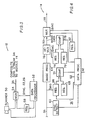
- Figure 1 shows a block diagram for an image processing apparatus constructed in accordance with the present invention;
- Figure 2 shows the combined data stream utilized in the apparatus of Figure 1;
- Figure 3 shows details of a data acquisition module for the apparatus of Figures 1 and 3; and
- Figure 4 shows details of an image processing module.
- Referring now to the Figures, an
apparatus 10 constructed in accordance with this invention, includes several modules, such as adata acquisition module 12, andimage processing modules - For each image to be represented on a video screen, the data is partitioned into blocks, each block being representative of a horizontal line across the screen. Several of these lines are assembled on a screen to form a frame.
- The sequential arrangement of the data blocks is illustrated in Figure 2. Each frame is started with a vertical sync signal (not shown). The vertical sync signal is followed by the end of a
horizontal sync signal 22, indicating the beginning of the image data for the first horizontal line. At the end ofimage data period 24 there is anotherhorizontal sync signal 26 indicating the beginning of a horizontal blanking period. In the present invention, this horizontal blanking period is used for the transmission ofdiagnostic data 28. The next horizontal block is again started with the ending of thehorizontal sync signal 22 and the processes continues until the frame is completed. The end of the frame is signified by a vertical sync signal (not shown). Thecomposite data stream 34 of Figure 2 is first generated by thedata acquisition module 12 and transmitted over avideo channel 36 to the firstimage processing module 14. Themodule 14 performs image processing on the composite stream and generates a second data stream for transmission onchannel 38 tomodule 16. Themodule 16 performs its own processing on the stream received frommodule 14 and generates another stream for transmission onchannel 40 tomodule 18, and so on. It should be understood that in Figure 1 a serial arrangement is shown for the various modules, it being understood that one or more modules may also be arranged in parallel to receive and/or transmit a data stream from a common channel. - In addition to the image processing step assigned to them, modules also analyze the data stream received and/or transmitted and generate corresponding
diagnostic signals CPU 48 for further analysis if required. - As shown in Figure 3, the
data acquisition module 12 could consists of anoptical scanner 50 which scans an object (not shown) line by line under the control of adata processor 52. Thescanner 50 then produces image data which is fed to a multiplexer (mux) 54. Each data line is preceded by async signal 22. The image data for a line is output from the multiplexer online 36 to theimage processing module 14.Module 12 also includes aregister 58 which holds diagnostic data and is coupled to themultiplexer 54. This diagnostic data is transmitted onchannel 36 during eachsync signal 26. A similar operation occurs at the end of each frame to generate acomposite data stream 34 as shown in Figure 2. - Figure 4 shows the elements of the
image processing module 14. It should be understood that the other modules contain and operate in the same manner except that they may perform a different image processing step on the image data. -
Module 14 includes async detector circuit 60 which is used to detect the sync signals of thecomposite data stream 36. When a sync signal is detected by this circuit, a corresponding signal is transmitted to adata processor 62 which operates the various elements of the module. Following theinitial sync signal 22, the image data for a line is provided to animage processing stage 64 which performs a preselected image processing step thereon (such as for example multiplication by a constant for amplitude compensation). - Following the line image data is the beginning of
sync signal 26 indicating horizontal blanking. During this period the diagnostic data from the composite data stream is fed to aregister 66. Anotherregister 68 contains reference signals corresponding to the diagnostic signals. The contents of the tworegisters comparator 70. The comparator compares the contents of the two registers and sends the results of this comparison toprocessor 62. The processor analyzes this result to determine if the data stream fromchannel 36 is acceptable or it has been corrupted. - The diagnostic data from
channel 36 is also fed to imageprocessor stage 64 which performs the same operation thereon as the operation performed on the line image data. The complete processed data stream is sent to ademultiplexer 72 which separates it into a processed image data stream and a processed diagnostic data stream. The diagnostic data stream is fed to aregister 74. Another register 76 contains reference, i.e. data corresponding to the diagnostic data fromchannel 36 when theimage processor stage 64 operates properly. The contents of the tworegisters 74, 76 are fed to acomparator 78.Comparator 78 compares the contents of the two registers and the results of the comparison are fed toprocessor 62.Processor 62 analyzes this result to determine of theimage processor stage 64 is operating properly. The analysis fromcomparators CPU 48 throughline 42. - The processed image data from
demultiplexer 72 are fed to amultiplexer 80. Themultiplexer 80 receives this image data, the sync signals fromprocessor 42 and new diagnostic data signals fromregister 82 to assemble a sequential composite image signal online 38 for thenext processor module 16 where the whole process is repeated for its own processing element as well as forchannel 38. - In the above embodiment a scanner was used to generate the image data. However, it should be understood that for the purposes of this invention, the image data may be generated by other well known sources, or alternatively it may be received from an external source. Moreover, the functions of various discrete components (such as
registers comparators 70, 78) may be performed by thedata processors 62. Similarly, the functions of thedata processor 62 may be incorporated intoCPU 48. Numerous other modifications may be made to the invention without departing from its scope as defined in the appended claims.
Claims (14)
- In an image processing apparatus, a module comprising :
input means for receiving input video composite data, said data including an input video image component, said input composite data including sequential input data blocks separated by blanking periods to define a two dimensional input video image for display on a video screen and an input diagnostic component, said input diagnostic component being received during said blanking periods;
image processing means for processing said input composite data to produce processed composite data, said processed composite data including a processed video image component formed of sequential processed video data blocks separated by said blanking periods and a processed diagnostic component during said blanking periods;
data storage means for storing a processed reference;
first comparator means for comparing said processed diagnostic component with said processed reference to generate a first comparator signal; and
data processing means receiving said first comparator signal to determine if said image processing means is operating properly. - The module of claim 1 wherein said data storage means includes an input reference, said module further comprising second comparator means for comparing said input reference and said input diagnostic component and generating a second comparator signal, said data processing means receiving said second comparator signal.
- The module of claim 1 wherein said data storage means further includes an output reference and said module further comprises output means for generating an output composite signal from said output reference and said processed image component, said output composite signal including said processed data blocks separated by said blanking periods and said output reference signal transmitted during said blanking periods.
- An image processing system comprising :(a) an image acquisition module including(i) a source of video image data, said image data being separated into image blocks, image separated by blanking periods, which image data defines a two dimensional video(ii) an input source of diagnostic data and(iii) interleaving means for interleaving diagnostic data between said video image blocks to provide composite input data having an input image component and an input diagnostic component with said input diagnostic component being transmitted during said blanking periods; and(b) an image processing module receiving said composite input data, and including(i) image processing means for processing said composite input data to generate composite processed data having a processed image component and a processed diagnostic component, said processed component being defined by processed data blocks separated by said blanking periods to form a two dimensional processed image, with said processed diagnostic component being positioned in said blanking periods,(ii) a processed reference source for generating a processed reference,(iii) processed comparing means for comparing said processed diagnostic component and said processed reference to generate a first comparator signal, and(iv) analyzing means for analyzing said first comparator signal to determine if said image processing means is functioning properly.
- The image processing system of claim 4 wherein said image processing means further includes an input reference source for generating an input reference, and input comparing means for comparing said input diagnostic component to said input reference to generate a second comparator single'for said analyzing means.
- The image processing system of claim 5 further comprising channel means for transmitting said input composite data to said image processing module.
- The image processing system of claim 6 wherein said analyzing means analyzes said second comparator signal to determine if said channel operates properly.
- The image processing system of claim 4 further comprising an output reference source for generating an output diagnostic component, and combining means for generating output composite data comprising said processed image component interleaved with said output diagnostic data.
- The image processing system of claim 8 and further comprising another image processing module receiving said output diagnostic data.
- The image processing system of claim 4 wherein said source of image data is an optical scanner.
- A method of monitoring an image processing system having a source of image data and an image processing element, comprising the steps of :
separating said image data into video image blocks partitioned by blanking periods to define a two dimensional video image;
interleaving said image blocks with input diagnostic data to form composite input data having an input image component and an input diagnostic component, said input diagnostic data being positioned in said blanking periods;
processing said composite input data with said image processing element to form processed composite data having a processed image component formed of processed data blocks separated by said blanking periods to generate a processed two-dimensional video image and a processed diagnostic component positioned in said blanking periods;
comparing said diagnostic component with a reference to generate a first comparator signal; and
analyzing said first comparator signal to monitor said processing. - The method of claim 11 wherein said source of image data is an optical scanner generating a two dimensional image composed of lines, wherein each said image block corresponds to one of said lines separated by one of said blanking periods, and wherein said diagnostic component is inserted in said one blanking period.
- The method of claim 11 further comprising the step of comparing said input diagnostic component with an input reference.
- The method of claim 11 further comprising the step of interleaving said processed data with an input reference to generate composite output data composed of said processed data blocks followed sequentially by an output diagnostic component during said blanking periods.
Applications Claiming Priority (2)
| Application Number | Priority Date | Filing Date | Title |
|---|---|---|---|
| US92677192A | 1992-08-06 | 1992-08-06 | |
| US926771 | 1992-08-06 |
Publications (3)
| Publication Number | Publication Date |
|---|---|
| EP0582546A2 true EP0582546A2 (en) | 1994-02-09 |
| EP0582546A3 EP0582546A3 (en) | 1995-09-06 |
| EP0582546B1 EP0582546B1 (en) | 1999-03-24 |
Family
ID=25453699
Family Applications (1)
| Application Number | Title | Priority Date | Filing Date |
|---|---|---|---|
| EP93810532A Expired - Lifetime EP0582546B1 (en) | 1992-08-06 | 1993-07-26 | Apparatus for monitoring image processing operations |
Country Status (10)
| Country | Link |
|---|---|
| US (1) | US5394486A (en) |
| EP (1) | EP0582546B1 (en) |
| JP (1) | JP3305819B2 (en) |
| KR (1) | KR100267452B1 (en) |
| CN (1) | CN1053778C (en) |
| AT (1) | ATE178149T1 (en) |
| AU (1) | AU665261B2 (en) |
| CA (1) | CA2100322C (en) |
| DE (1) | DE69324078T2 (en) |
| RU (1) | RU2138852C1 (en) |
Cited By (2)
| Publication number | Priority date | Publication date | Assignee | Title |
|---|---|---|---|---|
| RU2363975C2 (en) * | 2007-03-23 | 2009-08-10 | Открытое Акционерное Общество "Дольта" | Portable programmable-diagnostics complex |
| EP2305488A1 (en) | 2004-04-22 | 2011-04-06 | KBA-NotaSys SA | Laser perforating system and production process |
Families Citing this family (18)
| Publication number | Priority date | Publication date | Assignee | Title |
|---|---|---|---|---|
| JP3222522B2 (en) * | 1992-02-07 | 2001-10-29 | キヤノン株式会社 | Inspection system and method |
| CN1313959C (en) * | 1995-04-19 | 2007-05-02 | 吴乐南 | Four picture collector intelligent monitoring method |
| JPH09212139A (en) * | 1996-02-02 | 1997-08-15 | Sony Corp | Image display system |
| US5914846A (en) * | 1997-05-06 | 1999-06-22 | Tii Industries, Inc. | Cable interconnection apparatus for network interface device |
| US6219467B1 (en) * | 1997-07-15 | 2001-04-17 | Fuji Photo Film Co. Ltd. | Image processing device |
| US6457086B1 (en) * | 1999-11-16 | 2002-09-24 | Apple Computers, Inc. | Method and apparatus for accelerating detection of serial bus device speed signals |
| US7266617B1 (en) * | 2000-01-18 | 2007-09-04 | Apple Inc. | Method and apparatus for border node behavior on a full-duplex bus |
| US6639918B1 (en) | 2000-01-18 | 2003-10-28 | Apple Computer, Inc. | Method and apparatus for border node behavior on a full-duplex bus |
| US6618785B1 (en) * | 2000-04-21 | 2003-09-09 | Apple Computer, Inc. | Method and apparatus for automatic detection and healing of signal pair crossover on a high performance serial bus |
| US7668099B2 (en) * | 2003-06-13 | 2010-02-23 | Apple Inc. | Synthesis of vertical blanking signal |
| EP1519314A1 (en) * | 2003-09-25 | 2005-03-30 | Siemens Building Technologies AG | Method and analysis tool for checking functionality of video surveillance devices and measuring system for carrying out the method |
| EP1589495A1 (en) | 2004-04-22 | 2005-10-26 | Kba-Giori S.A. | Inspection machine and process |
| JP4929584B2 (en) * | 2004-11-04 | 2012-05-09 | ソニー株式会社 | Signal processing method, signal processing apparatus, and semiconductor device for detecting physical quantity distribution |
| US7773126B1 (en) * | 2006-05-26 | 2010-08-10 | Itt Manufacturing Enterprises, Inc. | Mosaic image collector including an embedded atomic clock |
| JP5588000B2 (en) * | 2009-07-06 | 2014-09-10 | ドイタ ヴェルケ ゲーエムベーハー | Method for displaying safety-related information on a display and apparatus to which the method is applied |
| CN103150564A (en) * | 2013-03-28 | 2013-06-12 | 冶金自动化研究设计院 | Plate surface code spraying character recognition device and method thereof |
| US20190018408A1 (en) * | 2017-07-12 | 2019-01-17 | Qualcomm Incorporated | Systems and methods for verifying integrity of a sensing system |
| CN110148283A (en) * | 2019-05-16 | 2019-08-20 | 安徽天帆智能科技有限责任公司 | It is a kind of to fall water monitoring system in real time based on convolutional neural networks |
Family Cites Families (24)
| Publication number | Priority date | Publication date | Assignee | Title |
|---|---|---|---|---|
| GB1532405A (en) * | 1974-11-01 | 1978-11-15 | Indep Broadcasting Authority | Television systems |
| JPS5534817A (en) * | 1978-08-31 | 1980-03-11 | Tokyo Electric Power Co | Converter |
| US4426698A (en) * | 1981-08-24 | 1984-01-17 | Eeco Incorporated | Television digital data frame with error detection |
| FR2523791B1 (en) * | 1982-03-19 | 1985-01-04 | Thomson Csf | DEVICE AND APPARATUS FOR TESTING ELECTRONIC EQUIPMENT, PARTICULARLY TELEVISION |
| CA1203631A (en) * | 1982-11-26 | 1986-04-22 | John L. Judge | Detecting improper operation of a digital data processing apparatus |
| EP0132453B1 (en) * | 1983-07-29 | 1987-05-27 | DR.-ING. RUDOLF HELL GmbH | Method and apparatus for minimizing errors during the digital processing of electric signals |
| JPS6081686A (en) * | 1983-10-11 | 1985-05-09 | Hitachi Ltd | Specifying circuit of area |
| AU560508B2 (en) * | 1984-02-15 | 1987-04-09 | Matsushita Electric Industrial Co., Ltd. | Pay tv delta encoded sound signal processing apparatus |
| DE3575646D1 (en) * | 1984-03-24 | 1990-03-01 | Philips Nv | METHOD FOR TRANSMITTING INFORMATION WITH ERROR CORRECTION FOR DATA WORDS, AN ERROR CORRECTION DECODING METHOD FOR SUCH DATA WORDS, AN ARRANGEMENT FOR INFORMATION TRANSFER FOR USE WITH THE METHOD, AND A METHOD FOR USING AN APPARATUS. |
| FR2566950B1 (en) * | 1984-06-29 | 1986-12-26 | Texas Instruments France | VIDEO IMAGE POINT PROCESSOR, VIEWING SYSTEM COMPRISING APPLICATION AND METHOD FOR IMPLEMENTING SAME |
| CA1254683A (en) * | 1985-05-17 | 1989-05-23 | Kevin P. Staggs | On-line verification of video display generator |
| US4700222A (en) * | 1985-05-30 | 1987-10-13 | Gill Industries, Incorporated | Apparatus and method of testing the frequency response of a cable television system |
| SU1309044A1 (en) * | 1985-12-13 | 1987-05-07 | Специальное Конструкторское Бюро Научного Приборостроения "Оптика" Со Ан Ссср | Device for processing images |
| JP2585535B2 (en) * | 1986-06-02 | 1997-02-26 | 株式会社日立製作所 | Process connection method in compound computer system |
| US4794600A (en) * | 1987-09-09 | 1988-12-27 | Eastman Kodak Company | Apparatus for error correction of digital image data by means of image redundancy |
| JPH0193933A (en) * | 1987-10-06 | 1989-04-12 | Sony Corp | Error correction encoder |
| US4894718A (en) * | 1989-03-29 | 1990-01-16 | Acer Incorporated | Method and system for testing video |
| EP0450023A1 (en) * | 1989-10-10 | 1991-10-09 | Unisys Corporation | Parallel pipelined image processor |
| JPH04196769A (en) * | 1990-11-27 | 1992-07-16 | Matsushita Electric Ind Co Ltd | Signal processor |
| US5136368A (en) * | 1991-01-24 | 1992-08-04 | The Grass Valley Group, Inc. | Television signal decoder with improved architecture |
| US5228042A (en) * | 1991-02-07 | 1993-07-13 | Northern Telecom Limited | Method and circuit for testing transmission paths |
| JPH04304082A (en) * | 1991-03-31 | 1992-10-27 | Sony Corp | Picture signal converting device |
| US5168216A (en) * | 1991-05-24 | 1992-12-01 | International Business Machines Corporation | System for testing high-speed digital circuits |
| JP3136565B2 (en) * | 1991-10-30 | 2001-02-19 | ソニー株式会社 | Video signal processing device |
-
1993
- 1993-07-12 CA CA002100322A patent/CA2100322C/en not_active Expired - Fee Related
- 1993-07-23 JP JP18266393A patent/JP3305819B2/en not_active Expired - Fee Related
- 1993-07-26 EP EP93810532A patent/EP0582546B1/en not_active Expired - Lifetime
- 1993-07-26 AT AT93810532T patent/ATE178149T1/en not_active IP Right Cessation
- 1993-07-26 DE DE69324078T patent/DE69324078T2/en not_active Expired - Lifetime
- 1993-07-27 AU AU44216/93A patent/AU665261B2/en not_active Ceased
- 1993-08-04 KR KR1019930015136A patent/KR100267452B1/en not_active Expired - Fee Related
- 1993-08-05 RU RU93049266A patent/RU2138852C1/en not_active IP Right Cessation
- 1993-08-05 CN CN93109652A patent/CN1053778C/en not_active Expired - Fee Related
-
1994
- 1994-06-29 US US08/268,657 patent/US5394486A/en not_active Expired - Lifetime
Cited By (3)
| Publication number | Priority date | Publication date | Assignee | Title |
|---|---|---|---|---|
| EP2305488A1 (en) | 2004-04-22 | 2011-04-06 | KBA-NotaSys SA | Laser perforating system and production process |
| US9849711B2 (en) | 2004-04-22 | 2017-12-26 | Kba-Giori S.A. | Printing machine with laser perforating |
| RU2363975C2 (en) * | 2007-03-23 | 2009-08-10 | Открытое Акционерное Общество "Дольта" | Portable programmable-diagnostics complex |
Also Published As
| Publication number | Publication date |
|---|---|
| JP3305819B2 (en) | 2002-07-24 |
| ATE178149T1 (en) | 1999-04-15 |
| RU2138852C1 (en) | 1999-09-27 |
| US5394486A (en) | 1995-02-28 |
| CA2100322C (en) | 2004-06-22 |
| CN1053778C (en) | 2000-06-21 |
| EP0582546A3 (en) | 1995-09-06 |
| JPH06176115A (en) | 1994-06-24 |
| AU665261B2 (en) | 1995-12-21 |
| KR940004475A (en) | 1994-03-15 |
| DE69324078D1 (en) | 1999-04-29 |
| CN1083647A (en) | 1994-03-09 |
| AU4421693A (en) | 1994-02-10 |
| KR100267452B1 (en) | 2000-10-16 |
| CA2100322A1 (en) | 1994-02-07 |
| DE69324078T2 (en) | 2000-01-05 |
| EP0582546B1 (en) | 1999-03-24 |
Similar Documents
| Publication | Publication Date | Title |
|---|---|---|
| EP0582546B1 (en) | Apparatus for monitoring image processing operations | |
| US6246435B1 (en) | In-service realtime picture quality analysis | |
| EP2509332B1 (en) | Automatic test system for digital display systems | |
| FI74176C (en) | Method and apparatus for synchronizing a microprocessor with one video signal | |
| US5367337A (en) | Method and apparatus for capturing video images | |
| US7023471B2 (en) | Video quality assessment with test video sequences | |
| WO2001051940A1 (en) | An algorithmic test pattern generator, with built-in-self-test (bist) capabilities, for functional testing of a circuit | |
| US7085408B1 (en) | Method and system for testing image sensor system-on-chip | |
| CN111741291A (en) | Screen test method, electronic device and storage medium | |
| EP1727376B1 (en) | Instrument for real-time video quality measurement | |
| CN114422777A (en) | Image recognition-based time delay testing method and device and storage medium | |
| CN106303451B (en) | The video processing unit output synchronism detection method and system of multi-display apparatus | |
| GB2336063A (en) | Colour frame phase alignment | |
| JPH11184445A (en) | Display image capturing method for display device, image display performance inspection method and device therefor | |
| JP2004242130A (en) | Signal generating device and method for measuring video / audio transmission time difference, and signal analyzing device and method | |
| JPH096943A (en) | Image processing device failure diagnosis method | |
| US7149954B2 (en) | Method and system for programmable field statistic for picture cyclic redundancy check (CRC) | |
| CN113612988A (en) | Method and device for automatically testing video delay and video transmission equipment | |
| US5325197A (en) | Television signal processing unit which provides monitoring during periods of the television signal to detect erroneous circuit operation | |
| CN118283228A (en) | Image processing device, image processing device testing method and image processing system | |
| JP2003289554A (en) | Failure diagnosis method for television camera device | |
| DE102012016544A1 (en) | Robot system, has synchronization judging portion judging whether camera is operated in synchronization with external horizontal synchronization signal based on temporary change of phase comparison result from phase comparison portion | |
| KR100200831B1 (en) | Inspection regulator of image signal output of printed circuit board for image signal and inspection adjustment method thereby | |
| KR20210065619A (en) | Image analysis apparatus | |
| JPH0927973A (en) | Failure diagnosis method for television camera device |
Legal Events
| Date | Code | Title | Description |
|---|---|---|---|
| PUAI | Public reference made under article 153(3) epc to a published international application that has entered the european phase |
Free format text: ORIGINAL CODE: 0009012 |
|
| AK | Designated contracting states |
Kind code of ref document: A2 Designated state(s): AT CH DE FR GB IT LI SE |
|
| PUAL | Search report despatched |
Free format text: ORIGINAL CODE: 0009013 |
|
| AK | Designated contracting states |
Kind code of ref document: A3 Designated state(s): AT CH DE FR GB IT LI SE |
|
| 17P | Request for examination filed |
Effective date: 19960223 |
|
| 17Q | First examination report despatched |
Effective date: 19970502 |
|
| GRAG | Despatch of communication of intention to grant |
Free format text: ORIGINAL CODE: EPIDOS AGRA |
|
| GRAG | Despatch of communication of intention to grant |
Free format text: ORIGINAL CODE: EPIDOS AGRA |
|
| GRAH | Despatch of communication of intention to grant a patent |
Free format text: ORIGINAL CODE: EPIDOS IGRA |
|
| GRAH | Despatch of communication of intention to grant a patent |
Free format text: ORIGINAL CODE: EPIDOS IGRA |
|
| GRAA | (expected) grant |
Free format text: ORIGINAL CODE: 0009210 |
|
| AK | Designated contracting states |
Kind code of ref document: B1 Designated state(s): AT CH DE FR GB IT LI SE |
|
| REF | Corresponds to: |
Ref document number: 178149 Country of ref document: AT Date of ref document: 19990415 Kind code of ref document: T |
|
| REG | Reference to a national code |
Ref country code: CH Ref legal event code: EP |
|
| ITF | It: translation for a ep patent filed | ||
| REF | Corresponds to: |
Ref document number: 69324078 Country of ref document: DE Date of ref document: 19990429 |
|
| ET | Fr: translation filed | ||
| PLBE | No opposition filed within time limit |
Free format text: ORIGINAL CODE: 0009261 |
|
| STAA | Information on the status of an ep patent application or granted ep patent |
Free format text: STATUS: NO OPPOSITION FILED WITHIN TIME LIMIT |
|
| 26N | No opposition filed | ||
| REG | Reference to a national code |
Ref country code: GB Ref legal event code: IF02 |
|
| PGFP | Annual fee paid to national office [announced via postgrant information from national office to epo] |
Ref country code: SE Payment date: 20090722 Year of fee payment: 17 Ref country code: AT Payment date: 20090724 Year of fee payment: 17 |
|
| REG | Reference to a national code |
Ref country code: CH Ref legal event code: PFA Owner name: BA-GIORI S.A. Free format text: KBA-GIORI S.A.#4, RUE DE LA PAIX#1003 LAUSANNE (CH) -TRANSFER TO- KBA-GIORI S.A.#AVENUE DU GREY 55 CASE POSTALE 347#1000 LAUSANNE 22 (CH) |
|
| PGFP | Annual fee paid to national office [announced via postgrant information from national office to epo] |
Ref country code: CH Payment date: 20100825 Year of fee payment: 18 |
|
| PGFP | Annual fee paid to national office [announced via postgrant information from national office to epo] |
Ref country code: IT Payment date: 20100723 Year of fee payment: 18 Ref country code: FR Payment date: 20100802 Year of fee payment: 18 Ref country code: DE Payment date: 20100816 Year of fee payment: 18 |
|
| PGFP | Annual fee paid to national office [announced via postgrant information from national office to epo] |
Ref country code: GB Payment date: 20100721 Year of fee payment: 18 |
|
| REG | Reference to a national code |
Ref country code: CH Ref legal event code: PFA Owner name: KBA-NOTASYS SA Free format text: KBA-GIORI S.A.#AVENUE DU GREY 55 CASE POSTALE 347#1000 LAUSANNE 22 (CH) -TRANSFER TO- KBA-NOTASYS SA#AVENUE DU GREY 55 CASE POSTALE 347#1000 LAUSANNE 22 (CH) |
|
| PG25 | Lapsed in a contracting state [announced via postgrant information from national office to epo] |
Ref country code: AT Free format text: LAPSE BECAUSE OF NON-PAYMENT OF DUE FEES Effective date: 20100726 |
|
| REG | Reference to a national code |
Ref country code: DE Ref legal event code: R082 Ref document number: 69324078 Country of ref document: DE Representative=s name: REBLE & KLOSE RECHTS- UND PATENTANWAELTE, DE Effective date: 20111222 Ref country code: DE Ref legal event code: R081 Ref document number: 69324078 Country of ref document: DE Owner name: KBA-NOTASYS SA, CH Free format text: FORMER OWNER: KBA-GIORI S.A., LAUSANNE, CH Effective date: 20111222 |
|
| REG | Reference to a national code |
Ref country code: CH Ref legal event code: PL |
|
| GBPC | Gb: european patent ceased through non-payment of renewal fee |
Effective date: 20110726 |
|
| REG | Reference to a national code |
Ref country code: FR Ref legal event code: ST Effective date: 20120330 |
|
| PG25 | Lapsed in a contracting state [announced via postgrant information from national office to epo] |
Ref country code: LI Free format text: LAPSE BECAUSE OF NON-PAYMENT OF DUE FEES Effective date: 20110731 Ref country code: CH Free format text: LAPSE BECAUSE OF NON-PAYMENT OF DUE FEES Effective date: 20110731 Ref country code: DE Free format text: LAPSE BECAUSE OF NON-PAYMENT OF DUE FEES Effective date: 20120201 Ref country code: FR Free format text: LAPSE BECAUSE OF NON-PAYMENT OF DUE FEES Effective date: 20110801 |
|
| REG | Reference to a national code |
Ref country code: DE Ref legal event code: R119 Ref document number: 69324078 Country of ref document: DE Effective date: 20120201 |
|
| PG25 | Lapsed in a contracting state [announced via postgrant information from national office to epo] |
Ref country code: IT Free format text: LAPSE BECAUSE OF NON-PAYMENT OF DUE FEES Effective date: 20110726 |
|
| PG25 | Lapsed in a contracting state [announced via postgrant information from national office to epo] |
Ref country code: GB Free format text: LAPSE BECAUSE OF NON-PAYMENT OF DUE FEES Effective date: 20110726 |
|
| PG25 | Lapsed in a contracting state [announced via postgrant information from national office to epo] |
Ref country code: SE Free format text: LAPSE BECAUSE OF NON-PAYMENT OF DUE FEES Effective date: 20100727 |