EP0580618B1 - Electroluminescent silicon device - Google Patents
Electroluminescent silicon device Download PDFInfo
- Publication number
- EP0580618B1 EP0580618B1 EP92907005A EP92907005A EP0580618B1 EP 0580618 B1 EP0580618 B1 EP 0580618B1 EP 92907005 A EP92907005 A EP 92907005A EP 92907005 A EP92907005 A EP 92907005A EP 0580618 B1 EP0580618 B1 EP 0580618B1
- Authority
- EP
- European Patent Office
- Prior art keywords
- silicon
- porous
- electroluminescent
- layer
- quantum wires
- Prior art date
- Legal status (The legal status is an assumption and is not a legal conclusion. Google has not performed a legal analysis and makes no representation as to the accuracy of the status listed.)
- Expired - Lifetime
Links
Images



Classifications
-
- H—ELECTRICITY
- H10—SEMICONDUCTOR DEVICES; ELECTRIC SOLID-STATE DEVICES NOT OTHERWISE PROVIDED FOR
- H10H—INORGANIC LIGHT-EMITTING SEMICONDUCTOR DEVICES HAVING POTENTIAL BARRIERS
- H10H20/00—Individual inorganic light-emitting semiconductor devices having potential barriers, e.g. light-emitting diodes [LED]
- H10H20/80—Constructional details
- H10H20/84—Coatings, e.g. passivation layers or antireflective coatings
-
- B—PERFORMING OPERATIONS; TRANSPORTING
- B82—NANOTECHNOLOGY
- B82Y—SPECIFIC USES OR APPLICATIONS OF NANOSTRUCTURES; MEASUREMENT OR ANALYSIS OF NANOSTRUCTURES; MANUFACTURE OR TREATMENT OF NANOSTRUCTURES
- B82Y10/00—Nanotechnology for information processing, storage or transmission, e.g. quantum computing or single electron logic
-
- B—PERFORMING OPERATIONS; TRANSPORTING
- B82—NANOTECHNOLOGY
- B82Y—SPECIFIC USES OR APPLICATIONS OF NANOSTRUCTURES; MEASUREMENT OR ANALYSIS OF NANOSTRUCTURES; MANUFACTURE OR TREATMENT OF NANOSTRUCTURES
- B82Y20/00—Nanooptics, e.g. quantum optics or photonic crystals
-
- H—ELECTRICITY
- H10—SEMICONDUCTOR DEVICES; ELECTRIC SOLID-STATE DEVICES NOT OTHERWISE PROVIDED FOR
- H10H—INORGANIC LIGHT-EMITTING SEMICONDUCTOR DEVICES HAVING POTENTIAL BARRIERS
- H10H20/00—Individual inorganic light-emitting semiconductor devices having potential barriers, e.g. light-emitting diodes [LED]
-
- H—ELECTRICITY
- H10—SEMICONDUCTOR DEVICES; ELECTRIC SOLID-STATE DEVICES NOT OTHERWISE PROVIDED FOR
- H10H—INORGANIC LIGHT-EMITTING SEMICONDUCTOR DEVICES HAVING POTENTIAL BARRIERS
- H10H20/00—Individual inorganic light-emitting semiconductor devices having potential barriers, e.g. light-emitting diodes [LED]
- H10H20/01—Manufacture or treatment
- H10H20/011—Manufacture or treatment of bodies, e.g. forming semiconductor layers
- H10H20/014—Manufacture or treatment of bodies, e.g. forming semiconductor layers having light-emitting regions comprising only Group IV materials
-
- H—ELECTRICITY
- H10—SEMICONDUCTOR DEVICES; ELECTRIC SOLID-STATE DEVICES NOT OTHERWISE PROVIDED FOR
- H10H—INORGANIC LIGHT-EMITTING SEMICONDUCTOR DEVICES HAVING POTENTIAL BARRIERS
- H10H20/00—Individual inorganic light-emitting semiconductor devices having potential barriers, e.g. light-emitting diodes [LED]
- H10H20/80—Constructional details
- H10H20/81—Bodies
- H10H20/811—Bodies having quantum effect structures or superlattices, e.g. tunnel junctions
- H10H20/812—Bodies having quantum effect structures or superlattices, e.g. tunnel junctions within the light-emitting regions, e.g. having quantum confinement structures
-
- H—ELECTRICITY
- H10—SEMICONDUCTOR DEVICES; ELECTRIC SOLID-STATE DEVICES NOT OTHERWISE PROVIDED FOR
- H10H—INORGANIC LIGHT-EMITTING SEMICONDUCTOR DEVICES HAVING POTENTIAL BARRIERS
- H10H20/00—Individual inorganic light-emitting semiconductor devices having potential barriers, e.g. light-emitting diodes [LED]
- H10H20/80—Constructional details
- H10H20/81—Bodies
- H10H20/822—Materials of the light-emitting regions
- H10H20/826—Materials of the light-emitting regions comprising only Group IV materials
- H10H20/8264—Materials of the light-emitting regions comprising only Group IV materials comprising polycrystalline, amorphous or porous Group IV materials
-
- H—ELECTRICITY
- H10—SEMICONDUCTOR DEVICES; ELECTRIC SOLID-STATE DEVICES NOT OTHERWISE PROVIDED FOR
- H10P—GENERIC PROCESSES OR APPARATUS FOR THE MANUFACTURE OR TREATMENT OF DEVICES COVERED BY CLASS H10
- H10P50/00—Etching of wafers, substrates or parts of devices
-
- Y—GENERAL TAGGING OF NEW TECHNOLOGICAL DEVELOPMENTS; GENERAL TAGGING OF CROSS-SECTIONAL TECHNOLOGIES SPANNING OVER SEVERAL SECTIONS OF THE IPC; TECHNICAL SUBJECTS COVERED BY FORMER USPC CROSS-REFERENCE ART COLLECTIONS [XRACs] AND DIGESTS
- Y10—TECHNICAL SUBJECTS COVERED BY FORMER USPC
- Y10S—TECHNICAL SUBJECTS COVERED BY FORMER USPC CROSS-REFERENCE ART COLLECTIONS [XRACs] AND DIGESTS
- Y10S977/00—Nanotechnology
- Y10S977/902—Specified use of nanostructure
- Y10S977/932—Specified use of nanostructure for electronic or optoelectronic application
- Y10S977/949—Radiation emitter using nanostructure
- Y10S977/95—Electromagnetic energy
Definitions
- This invention relates to an electroluminescent silicon device.
- Visible electroluminescence has also been observed from metal-silicon dioxide-silicon structures in which the silicon dioxide layer contains very small silicon crystallites (less than 50 ⁇ wide). This is described by Di Maria et al in "Electroluminescence Studies in Silicon Dioxide Films Containing Tiny Silicon Islands", J. Appl. Phys., Vol 56, p401 (1984). Again the emission has very low efficiency, typically less than 10 -6 photons per electron.
- the present invention provides an electroluminescent silicon device characterised in that the device is a composite structure comprising a porous silicon layer having quantum wires with surface passivation and a conducting material.
- the present invention provides an electroluminescent silicon device characterised in that it includes a composite structure of silicon material incorporating a porous region containing surface passivated quantum wires, and conductive material within the porous region, wherein the conductive material:
- surface passivation and “surface passivated” used herein relate to the creation of a surface with a low density of non-radiative recombination centres. Further details are obtainable from Phys Rev Letters, Vol 57, p 249, 1986. Embodiments of the invention have been observed to exhibit electroluminescence at a low bias voltage with a degree of stability greatly exceeding that characterising prior art devices based on anodic oxidation of silicon.
- the invention provides an electroluminescent silicon device characterised in that it includes a composite structure of silicon material incorporating a porous region containing surface passivated quantum wires, and conductive material within the porous region, wherein the conductive material:
- the present invention provides an electroluminescent silicon device characterised in that it includes a composite structure comprising a porous silicon layer having quantum wires with surface passivation and a conductive material, which conductive material:
- the composite structure is preferably capable of supporting a current density of at least 1mAcm -2 under a bias voltage of not more than 10 Volts, desirably not more than 5 Volts.
- the conductive material may be an electrolyte, a metal or a semi-metal.
- the porous silicon may be produced by creating pores in heavily doped n type or p type silicon material having a dopant impurity concentration which is greater than 1x10 18 cm -3 and not greater than 1x10 21 cm -3 . It may alteratively be produced by creating pores in lightly doped n type or p type silicon material having a dopant impurity concentration in the range 1x10 11 cm -3 to 1x10 18 cm -3 .
- the present invention provides a method of making an electroluminescent silicon device characterised in that it includes the formation of a composite structure comprising a porous silicon layer having quantum wires with surface passivation and a conducting material.
- the formation of the composite structure may include electroplating of a metal into the porous silicon layer; alternatively it may include introduction of an electrolyte into the porous silicon layer.
- the present invention provides a method of making an electroluminescent silicon device characterised in that it includes:
- the step of pervading the porous silicon with a conductive material may comprise an electrochemical procedure for introducing conductive material into the porous silicon; it may comprise electroplating metal into the porous silicon.
- the step of forming the porous silicon may include creating pores in heavily doped n type or p type silicon material having a dopant impurity concentration which is greater than 1x10 18 cm -3 and not greater than 1x10 21 cm -3 .
- the step of forming the porous silicon may alteratively include creating pores in lightly doped n type or p type silicon material having a dopant impurity concentration in the range 1x10 11 cm -3 to 1x10 18 cm -3 .
- the invention also provides an electroluminescent silicon device made by the foregoing method.
- the device is indicated generally by 10. It incorporates a silicon structure 12 produced from a silicon wafer 400 ⁇ m thick with an original upper surface indicated by a dotted line 12A and a lower surface 12B.
- the silicon structure 12 incorporates a bulk silicon layer 14 and a porous silicon layer 16.
- the bulk silicon layer 14 is very nearly the same thickness as the original wafer, and is shown vertically foreshortened as indicated by chain lines 14A.
- the porous silicon layer 16 has a thickness in the range 0.1 to 50 ⁇ m.
- the expression "layer” is a misnomer, because the layers 14 and 16 are not produced by deposition, but this terminology is normal in the art for strata of a device.
- the fabrication of silicon structures such as the structure 12 is described by L T Canham in "Silicon Quantum Wire Array Fabrication by Electrochemical and Chemical Dissolution of Wafers", Appl. Phys. Lett., Vol 57, p1046, (1990).
- the porous silicon layer 16 has been subjected to sufficient dissolution to produce pore merging to define isolated quantum wires such as 18 with pores such as 20 therebetween.
- the quantum wires 18 are upstanding from the bulk silicon layer 14. They are not of a regular shape, nor of a constant width, and pore size is greater than wire size; the wires 18 and pores 20 are shown schematically in Figure 1 in the interests of illustrational simplicity.
- the device 10 incorporated a silicon structure 12 produced from a heavily doped n-type (n + ) silicon wafer with an arsenic donor concentration of 5x10 18 cm -3
- the porous layer 16 had a porosity of 78% and a thickness of 13 ⁇ m, and had been aged in air for 17 months after its formation.
- the porous silicon layer 16 emitted visible (orange) photoluminescence when irradiated with ultra violet light.
- exposed surfaces of the bulk layer 14 and wires 18 had an oxidised silicon hydride surface layer 22.
- a surface layer such as the layer 22 provides surface passivation for underlying silicon quantum wires because it has a low density of non-radiative recombination centres.
- the wires 18 were immersed in an electrolyte 24 to form a composite electrolyte/semiconductor structure 25 in combination with the silicon structure 12.
- the electrolyte 24 was an aqueous solution of H 2 SO 4 :Na 2 S 2 O 8 with concentrations 0.5M:0.1M.
- a platinum electrode 26 was immersed in the electrolyte 24, and an Ohmic electrical connection 28 was provided to the bulk silicon layer 14.
- Porous silicon layers, consisting of quantum wires, such as the layer 16 have high electrical resistivity in the absence of an electrolyte 24. Treating the layer 16 as a continuous medium, an electrical resistivity can be defined, and typical values of resistivity several orders of magnitude greater than 10 6 Ohmcm have been measured for it. Consequently, in the absence of an electrolyte 24, the silicon structure 12 is highly resistive in directions parallel to arrows 29 perpendicular to the layers 14 and 16. However, when the device 10 was biased such that the silicon structure 12 was negative and formed the cathode and the platinum electrode 26 was positive and formed the anode, the device passed an appreciable current density, of the order of a few mAcm -2 , at bias voltages of less than 5 volts.
- This bias polarity corresponded to a forward biased silicon structure 12.
- a geometrical area of 1 cm 2 of the upper surface of the porous layer 16 was exposed to electrolyte, all other surface regions of the structure 12 having been masked.
- Current flowing between the platinum electrode 26 and structure 12 was then a few mA.
- Current density was calculated as the ratio of current to geometrical area, ignoring internal surface area of pores.
- this embodiment of the device 10 emitted orange electroluminescence which was visible to the naked eye. The electroluminescent emission was observed to be stable in that no diminution of electroluminescence was observable to the naked eye over a test period of several hours.
- the silicon structure 32 consists of an unetched part 34 of a bulk silicon wafer with thickness in the range 350-400 ⁇ m (shown in part only); the part 34 is referred to hereinafter as the "wafer 34".
- a silicon quantum wire layer 36 extends from the wafer 34, and is in the range 0.1 to 50 ⁇ m in thickness. The latter contains individual quantum wires such as 38 typically 2.5 nm in diameter.
- Figure 2 illustrates wire connectivity and branching, and is a better diagrammatic representation of quantum wires produce by pore overlap than the equivalent wires 18 in the porous layer 16 in Figure 1. However, silicon quantum wires have been observed to have microscopic roughness and undulating diameter which is not illustrated.
- a second embodiment of the device 10 was constructed from a lightly doped n-type (n - ) silicon wafer with an arsenic donor concentration of 5x10 15 cm -3 .
- the porous layer 16 had a porosity of 76%, a thickness of 0.4 ⁇ m and had been aged in air for 17 months prior to immersion in electrolyte.
- the electrolyte was as used in the previous embodiment. When biased, with the silicon structure as the cathode, with a bias voltage of 1 Volt or greater, visible orange electroluminescence was observed.
- a third embodiment of the device 10 was constructed from a heavily doped p-type (p + ) silicon wafer with a boron acceptor concentration of 5x10 18 cm -3 .
- the porous layer 16 had a porosity of 75% and a thickness of 4.3 ⁇ m, and had been aged in air for 15 months prior to immersion in electrolyte.
- the electrolyte was as in earlier embodiments.
- a fourth embodiment of the device 10 was constructed from a heavily doped p-type (p + ) silicon wafer with a boron acceptor concentration of 5x10 18 cm -3 once more.
- the porous layer 16 had a porosity of 72% and a thickness of 1.2 ⁇ m, and had been aged for 16 months.
- this embodiment was biased with the silicon structure as the cathode, and a bias voltage of 5 Volts or greater, it also exhibited visible orange electroluminescence.
- a device was constructed which was equivalent to the device 10 except that it had a porosity which was deliberately arranged to be too low to produce a significant density of quantum wires.
- This comparison device was constructed from a heavily doped n-type (n + ) silicon wafer with an arsenic donor concentration of 5x10 18 cm -3 . It had a porous silicon layer with a porosity of 44% and a thickness of 5 ⁇ m, and had been aged in air for 17 months. It incorporated the same electrolyte and electrical connections as the device 10, and differed from the latter in the thickness and porosity of the porous silicon layer. It did not exhibit visible electroluminescence under cathodic bias with bias voltages up to 30 Volts. Moreover, the porous silicon layer in the comparison device did not exhibit visible photoluminescence either. This is believed to be due its much lower porosity (compared to the like for the device 10) indicating that it did not incorporate isolated quantum wires to any significant extent.
- the material in which the silicon quantum wires are immersed need not be an electrolyte, but may be a conducting material such as a semiconductor, a semi-metal, a metal or a conducting polymer. Whether it is an electrolyte or a conducting material of another kind, the material contacting the quantum wires should conform to certain criteria. These criteria are discussed below. They provide tests for suitability of conducting materials for incorporation in devices of the invention.
- the conductive material should be amenable to a procedure for infiltration into the porous silicon layer 16 operative at low temperatures, i.e. below 300°C.
- the surface passivation layer 22 is degraded, and photoluminescence from the porous layer 16 becomes wholly or partially quenched.
- the porous layer 16 may begin to restructure itself increasing the width of the wires 18 and reducing their number. In consequence the quantum confinement of carriers may become lost.
- device production at higher temperatures is feasible if surface passivation and quantum confinement do not suffer serious degradation or if any such degradation is subsequently counteracted.
- the conductive material should have a reasonable conductivity; however, it is not appropriate to define a minimum bulk conductivity which the material must have to be suitable for infiltration into the porous silicon layer. This is due to the conductivity of materials differing between their bulk states and their presence within pores. It is more appropriate to define a minimum current density that should be supported by the composite structure 25 (the combination of the silicon structure 12 and the conductive material 24). Indeed, the composite structure 25 should be sufficiently conductive to support current densities of the order of, or greater than, 1 mAcm -2 at less than 10 Volts forward bias. Here current density is measured as previously described.
- the conductive material 24 It must be possible either substantially to fill the pore volume with the conductive material, or at least to pervade the pore volume sufficiently for the material to be electrically continuous as described below. There must be good electrical connection between the electrical contact to the material (e.g. the electrode 26) and the bulk silicon. For this to be the case, it is not necessary for the conductive material to form a physically continuous layer which completely covers the surface layer 22. It is for example sufficient to form a network of the conductive material producing a good connection between the electrode and the silicon structure 12. The important thing is that the conductive material 24 provide contact to a substantial proportion of the quantum wire surfaces, enabling current to flow in the wires 18 under bias as required for electroluminescence to occur.
- the conductive material 24 enables substantial current densities to flow in the composite structure 25 at low voltages, eg less than 10 Volts.
- the conductive material 24 ensures that an electrically continuous conductive path is established from one device terminal (the electrode 26) to the other device terminal (the Ohmic connection 28) through the conductive material 24, the quantum wires 18 and the bulk silicon 14.
- the conductive material 24 should form a stable interface with the oxidised silicon hydride surface layer 22, and should not significantly degrade the surface passivation provided by that layer. That is the porous layer 16 should still be capable of exhibiting photoluminescence after the conductive material has been infiltrated into the pores 20.
- the conductive material should be capable of providng an enhanced density of minority carriers in the silicon quantum wires 18 when the device 10 is at low bias voltage. It may acheive this by injection of minority carriers with adequate efficiency into the quantum wires 18. Injection efficiency is frequently quantified using a minority carrier injection ratio g, defined as the ratio of the minority carrier current to the total current passing across the relevant junction, as described by S M Sze in "Physics of Semiconductor Devices", Wiley and Sons, New York (1981) p268.
- g defined as the ratio of the minority carrier current to the total current passing across the relevant junction
- the density of minority carriers in the quantum wires 18 may also be enhanced by hot carrier-induced impact ionisation. Hot majority carriers accelerated by high electric fields can create electron-hole pairs by across-the-band gap ionisation.
- a particular carrier type which is the majority carrier type, is responsible for the major proportion of the current flowing in the silicon quantum wires 18 under applied bias. Minority carriers have opposite sign to majority carriers. Recombination of majority and minority carriers is believed to occur in the quantum wires 18, since electroluminescence is observed in them in embodiments of the invention. Since the quantum wires 18 have high resistivity as previously described, they do not appear to retain the electrical characteristics of the original silicon wafer from which they were formed. Consequently, the majority carrier type of the bulk silicon 14 (n type or p type) may the same as or opposite to that of the charge carriers giving rise to the majority carrier current flow in the quantum wires 18.
- Normal metal-semiconductor junctions usually exhibit very low minority carrier injection ratios, i.e. 10 -5 ⁇ g ⁇ 10 -3 .
- minority carrier injection ratios i.e. 10 -5 ⁇ g ⁇ 10 -3 .
- N D 10 16 cm -3
- Incorporation of a thin insulating layer between the metal and semiconductor layers, to form a Metal-Insulator-Semiconductor (MIS) junction can increase the minority carrier injection ratio under low bias.
- MIS Metal-Insulator-Semiconductor
- minority carriers must be injected from the conductive material 24 into the silicon quantum wires 18.
- Published data described above relates to bulk silicon in various circumstances; there are no data published for the injection of minority carriers into silicon quantum wires.
- the material 24 should be capable of producing an injection ratio g into the wires 18, of at least 10 -4 at bias voltages of 10 Volts or less.
- a material for which the injection ratio g is at least 10 -4 at bias voltages at or below 10 Volts is capable of efficiently injecting minority carriers for the purposes of this specification.
- Devices of the invention may be made from heavily doped n type or p type silicon material having a dopant impurity concentration which is greater than 1x10 18 cm -3 and not greater than 1x10 21 cm -3 . They may also be made from lightly doped n type or p type silicon material having a dopant impurity concentration in the range 1x10 11 cm -3 to 1x10 18 cm -3 .
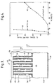
- FIG. 3 there is schematically shown a device of the invention indicated generally by 40 and incorporating conductive material in the form of metallisation. Laterally outer regions of the device 40 have been omitted as indicated by irregular edges such as 40A.
- the device 40 is shown in idealised form equivalent to Figure 1. It includes a silicon structure 42 incorporating a bulk silicon wafer 44 and a porous silicon layer 46.
- the wafer 44 has a central region which is foreshortened as indicated by dotted lines 44A.
- the porous layer 46 is electroplated with metal 48, which replaces the electrolyte 24 of earlier embodiments.
- the porous layer 46 incorporates quantum wires such as 50 each with an interfacial oxide layer such as 52.
- the metal 48 forms a layer on the oxide 52, and has discontinuities in it such as holes 54.
- the porous layer 46 is surmounted by a semitransparent conducting electrode layer 56, and the wafer 44 has an Ohmic contact 58.
- a first embodiment of the device 40 was made as follows from a p + silicon wafer with a boron acceptor concentration of 4x10 18 cm -3 .
- the wafer was anodised in an electrolyte (hereinafter called electrolyte I) containing equal volumetric proportions of ethanol and an HF/water solution, the latter containing 40% by weight of HF.
- Anodisation was carried out at a current density of 100 mAcm -2 for 15 sacs in the dark.
- This produced a porous layer 46 with a thickness of 1 ⁇ m which was then annealed in air at 240°C for 20 mins.
- the porous layer 46 gave visible photoluminescence under UV irradiation.
- porous layer upper surface was then masked to expose only an area of 9 mm 2 .
- Gold was electroplated into this area of the porous layer 46 from an aqueous solution containing 10gm/litre of AuCl 3 and 2.9 gm/litre NaCl.
- a platinum anode was used.
- a current density of 10 mAcm -2 was applied for a time of 45 seconds. This produced a composite of porous silicon plated with gold surmounted by a gold film about 0.2 ⁇ m thick.
- Electroluminescence indicated by photomultiplier current in nanoAmps is plotted against bias voltage.
- Graphs 60 and 62 relate to the gold plated embodiment of the invention and to the comparison non-plated porous layer respectively.
- the graph 60 shows that the gold plated embodiment exhibits electroluminescence at bias voltages above 3 Volts, and electroluminescence increases rapidly with increasing bias voltage.
- the graph 62 shows that the non-plated porous layer exhibits no significant electroluminescence at bias voltages below 10 Volts, and electroluminescence increases only slowly with increasing bias voltage thereafter.
- the porous layer requires 60 Volts bias to exhibit electroluminescence shown by the gold plated embodiment at only about 8 Volts.
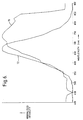
- FIG. 6 there is shown a graph 70 of electroluminescence emission in arbitrary units plotted as a function of wavelength in nm for the gold plated embodiment of the invention referred to above.
- the graph 70 indicates that electroluminescence emission is largely in the range 550-850nm, centred at about 760nm. Blue light from an He-Cd laser was used to obtain photoluminescence from the comparison non-plated porous layer referred to above, and this provided a second graph 72 in Figure 6.
- the graph 72 indicates that photoluminescence emission in the absence of plated metal was largely in the range 550-790nm, centred at about 660nm.
- the electroluminescence emission is therefore spectrally broader and shifted to longer wavelengths compared to the photoluminescence emission of the comparison layer.
- Both graphs 70 and 72 have normalised intensity values calculated by dividing actual intensity by peak intensity throughout.
- the first embodiment of the device 40 had an overlying gold film 0.2 ⁇ m thick, which is undesirably thick from the point of view of obtaining transparency to visible light.
- the composite was subjected to a low energy Argon ion etch to remove the overlying gold film. This greatly improved the visible photoluminescence obtainable from the porous layer 46 under blue laser irradiation.
- a second embodiment of the device 40 was made as follows from an n + silicon wafer with an arsenic donor concentration of 8x10 18 cm -3 .
- the wafer was anodised in electrolyte I at a current density of 7.5 mAcm -2 for 10 mins in the dark. It was then subjected to chemical dissolution at 27°C for 6 hours in a second electrolyte containing equal volumetric proportions of ethanol and an HF/water solution, the latter containing 20% by weight of HF. It was then annealed in air at 200°C for 2 hours.
- Fourier transform infra-red spectroscopy (FTIR) indicates that the anneal step produces a silicon oxide layer on exposed silicon surfaces.
- a further embodiment of the invention was produced which was equivalent to the device 40, except that it was not annealed to produce an oxide layer 52. It was made as follows from an n + silicon wafer with an arsenic donor concentration of 8x10 18 cm -3 . The wafer was anodised in electrolyte I at a current density of 7.5 mAcm -2 for 10 mins in the dark. It was then subjected to chemical dissolution at 27°C for 5 hours in electrolyte I. This series of steps produced a porous layer which gave visible photoluminescence under UV irradiation. The porous layer upper surface was then masked to expose an area of 9 mm 2 .
- Tin was electroplated into this area of the porous layer 66 from an acidic (H 2 SO 4 ) aqueous solution containing 13 gm/litre of SnSO 4 , 0.4 gm/litre of gelatin, 0.2 gm/litre of ⁇ -naphthene and 50 vol.% ethanol.
- a pure tin anode was used.
- a current density of 1 mAcm -2 was applied for a time of 30 mins. This produced a composite of porous silicon plated with tin surmounted by a grey film of tin. The composite was dried at 110°C for 10 mins. Electroluminescence was obtained from this embodiment after electroding and under bias as described for earlier embodiments.
- Electroplating of tin into a porous layer of heavily doped n-type silicon of approximately 5 ⁇ m thickness was also carried out for the purposes of investigating evenness of the distribution of tin as a function of depth.
- Electroplating of metal into porous silicon is known to be difficult to acheive with acceptable depth uniformity. This is described by R Herino, P Jan and G Bomchil in "Nickel Plating on Porous Silicon", J. Electrochem. Soc.:Solid-State Science and Technology, Vol 132, p2513 (1985); their results show that they encountered difficulty in obtaining an even depth distribution of nickel through porous layers thicker than 1 ⁇ m or so.
- an aged porous silicon test layer (porosity 64%) and a pure tin anode were immersed in a HCl/SnCl 2 electroplating solution.
- a bias voltage was applied with a polarity appropriate for the silicon to form the cathode.
- the current density was gradually ramped up from a few ⁇ Acm -2 to a few mAcm -2 over a period of the order of eight hours.
- results of a Secondary Ion Mass Spectroscopy (SIMS) analysis showing tin deposition throughout a relatively thick porous silicon test layer are illustrated graphically.
- Curve 80 shows the distribution of 30 Si with depth, curve 82 that of 116 Sn, curve 84 that of 118 Sn and curve 86 that of 120 Sn.
- Curve 80 has a dip 80a at the point corresponding to the thickness of the porous test layer.
- the curves 82, 84 and 86 show that tin has been deposited fairly uniformly through the greater proportion of the thickness of the porous test layer.
- SIMS is susceptible to interference.
- the ratio of measured 120 Sn to measured 118 Sn within the thickness of the porous test layer was calculated. The ratio was found to be 1.4 which is correct for naturally occurring tin.
- the porous silicon test layer Prior to electroplating, the porous silicon test layer exhibited visible photoluminescence when under ultra violet illumination. After being electroplated with tin the porous test layer still exhibited this photoluminescence, which indicated that the surface passivation of the test layer had not been significantly degraded by the process.
- the method of electroplating a metal into porous silicon layers consisting of quantum wires is not limited to the impregnation of gold and tin.
- the electroplating solution used must wet the pores sufficiently, at least under bias when electrocapillarity occurs, for an electrically continuous layer of the metal to be formed.
- electroplating may be performed in the same solution as fabrication of the quantum wire array by etching of a porous silicon layer. This provides the advantage of not requiring a delicate silicon structure to be removed from the etching solution and dried before further processing is performed.
- surface passivation may be performed entirely by eletrochemical processing, instead of partly by such processing followed by ageing or annealing in air or in a gaseous or vapour medium of another kind.
Landscapes
- Engineering & Computer Science (AREA)
- Nanotechnology (AREA)
- Chemical & Material Sciences (AREA)
- Crystallography & Structural Chemistry (AREA)
- Physics & Mathematics (AREA)
- Optics & Photonics (AREA)
- Biophysics (AREA)
- Life Sciences & Earth Sciences (AREA)
- Mathematical Physics (AREA)
- Theoretical Computer Science (AREA)
- Led Devices (AREA)
- Crystals, And After-Treatments Of Crystals (AREA)
- Led Device Packages (AREA)
- Electroluminescent Light Sources (AREA)
Abstract
Description
- This invention relates to an electroluminescent silicon device.
- There is considerable interest in the production of silicon-based or silicon-compatible light emitting devices for use in opto-electronic integrated circuits. In the course of work to develop such devices, visible electroluminescence has been observed from silicon in a variety of circumstances some of which are described briefly below.
- R Newman in "Visible Light from Silicon p-n Junction", Phys. Rev. Vol 100, p700 (1955) and Chynoweth and McKay in "Photon Emission from Avalanche Breakdown in Silicon", Phys. Rev., Vol 102, p369 (1956) describe very broad band electroluminescent emission when bulk silicon p-n junctions are reverse biased to "avalanche breakdown". The emission extends from about 3eV to below 1eV and is of very low efficiency, typically 10-5 photons per electron.
- Visible electroluminescence has also been observed from metal-silicon dioxide-silicon structures in which the silicon dioxide layer contains very small silicon crystallites (less than 50Å wide). This is described by Di Maria et al in "Electroluminescence Studies in Silicon Dioxide Films Containing Tiny Silicon Islands", J. Appl. Phys.,
Vol 56, p401 (1984). Again the emission has very low efficiency, typically less than 10-6 photons per electron. - W Waring and E A Benjamin in "Luminesence during Anodic Oxidation of Silicon", J. Electrochem. Soc., Vol 11, p1256 (1964) describe visible electroluminescence from bulk silicon surfaces when they are anodically biased in electrolytes capable of oxidising the surface. Once again the efficiency of the emission is low, and in addition it is unstable since it results from chemical changes at the relevant interface. More recent work in this field is described by A P Baraban et al in "Electroluminescence Spectra in the System Silicon-Silicon Dioxide-Electrolyte", Soviet Electrochem.,
Vol 20, p507 (1984). - A Gee in "Electrochemiluminescence at a Silicon Anode in Contact with an Electrolyte", J. Electrochem. Soc., Vol 107, p787 (1960) describes visible electroluminescence from chemically produced stain films on bulk p-type silicon under anodic bias in many electrolytes. The emission of the light results from the anodic oxidation of the film and is irreversible.
- The above approaches to obtaining electroluminescence from silicon therefore have a number of drawbacks, primarily very low efficiency or irreversibility. These drawbacks render the approaches unsuitable for producing practical electroluminescent silicon devices.
- Recently L T Canham in "Silicon Quantum Wire Array Fabrication by Electrochemical and Chemical Dissolution of Wafers", Appl. Phys. Lett., Vol 57, p1046, (1990), describes the fabrication of free standing silicon quantum wire arrays in surface layers of bulk silicon wafers. Free standing wires are taken to be wires which are not immersed or embedded in another material. The wires themselves need not be isolated columns but may be interlinked. Quantum wires are wires in which the diameter is sufficiently small such that quantum confinement of carriers occurs within them. The result of this is that the bandgap of the material concerned, in this case silicon, is significantly increased. Visible red photoluminescence is emitted from these quantum wire arrays under appropriate irradiation. These arrays are however highly resistive and therefore unlikely to yield significant electroluminescence at the low applied bias voltages required for conventional integrated circuitry. This work has been reproduced elsewhere, and workers have gone on to suggest that appropriately doped free standing silicon quantum wires would provide an array of lower resistivity capable of supporting appreciable current and exhibiting electroluminescence. Despite this, there has been no report of silicon quantum wires which are doped appropriately for the above electroluminescent behaviour to be exhibited.
- It is an object of the invention to provide an alternative form of electroluminescent silicon device.
- In one aspect, the present invention provides an electroluminescent silicon device characterised in that the device is a composite structure comprising a porous silicon layer having quantum wires with surface passivation and a conducting material.
- In another aspect, the present invention provides an electroluminescent silicon device characterised in that it includes a composite structure of silicon material incorporating a porous region containing surface passivated quantum wires, and conductive material within the porous region, wherein the conductive material:
- (a) is arranged to enhance conduction through the quantum wires,
- (b) does not degrade the quantum wire surface passivation sufficiently to render the quantum wires non-luminescent, and
- (c) is arranged to enhance the minority carrier density within the quantum wires.
- The expressions "surface passivation" and "surface passivated" used herein relate to the creation of a surface with a low density of non-radiative recombination centres. Further details are obtainable from Phys Rev Letters, Vol 57, p 249, 1986. Embodiments of the invention have been observed to exhibit electroluminescence at a low bias voltage with a degree of stability greatly exceeding that characterising prior art devices based on anodic oxidation of silicon.
- In an additional aspect, the invention provides an electroluminescent silicon device characterised in that it includes a composite structure of silicon material incorporating a porous region containing surface passivated quantum wires, and conductive material within the porous region, wherein the conductive material:
- (a) is arranged to ensure that an electrically continuous current path extends through the porous region,
- (b) does not degrade the quantum wire surface passivation sufficiently to render the quantum wires non-luminescent, and
- (c) is arranged to inject minority carriers into the quantum wires.
- In another aspect, the present invention provides an electroluminescent silicon device characterised in that it includes a composite structure comprising a porous silicon layer having quantum wires with surface passivation and a conductive material, which conductive material:
- (a) forms an electrically continuous layer over the internal surface of the porous silicon layer,
- (b) does not significantly degrade the surface passivation of the porous silicon layer, and
- (c) is capable of efficiently injecting minority carriers into the quantum wires.
- The composite structure is preferably capable of supporting a current density of at least 1mAcm-2 under a bias voltage of not more than 10 Volts, desirably not more than 5 Volts.
- The conductive material may be an electrolyte, a metal or a semi-metal.
- The porous silicon may be produced by creating pores in heavily doped n type or p type silicon material having a dopant impurity concentration which is greater than 1x1018cm-3 and not greater than 1x1021cm-3. It may alteratively be produced by creating pores in lightly doped n type or p type silicon material having a dopant impurity concentration in the range 1x1011cm-3 to 1x1018cm-3.
- In an alternative aspect, the present invention provides a method of making an electroluminescent silicon device characterised in that it includes the formation of a composite structure comprising a porous silicon layer having quantum wires with surface passivation and a conducting material.
- The formation of the composite structure may include electroplating of a metal into the porous silicon layer; alternatively it may include introduction of an electrolyte into the porous silicon layer.
- In an alternative aspect, the present invention provides a method of making an electroluminescent silicon device characterised in that it includes:
- (a) forming porous silicon incorporating quantum wires with surface passivation, and
- (b) pervading the porous silicon with a conductive material arranged to enhance electrical conduction therethrough without rendering the quantum wires non-luminescent.
- The step of pervading the porous silicon with a conductive material may comprise an electrochemical procedure for introducing conductive material into the porous silicon; it may comprise electroplating metal into the porous silicon.
- The step of forming the porous silicon may include creating pores in heavily doped n type or p type silicon material having a dopant impurity concentration which is greater than 1x1018cm-3 and not greater than 1x1021cm-3. The step of forming the porous silicon may alteratively include creating pores in lightly doped n type or p type silicon material having a dopant impurity concentration in the range 1x1011cm-3 to 1x1018cm-3.
- The invention also provides an electroluminescent silicon device made by the foregoing method.
- In order that the invention may be more fully understood, embodiments thereof will now be described, by way of example only, with reference to the accompanying drawings, in which:
- Figure 1
- illustrates schematically a vertical cross-section through an electroluminescent silicon device of the invention;
- Figure 2
- illustrates connectivity and branching in quantum wires;
- Figure 3
- illustrates schematically a vertical cross-section through a device of the invention incorporating metal electroplated into a porous silicon layer; and
- Figures 4 and 5
- graphically illustrate electroluminescence and conduction properties of a device in accordance with Figure 3 and a comparison device;
- Figure 6
- graphically illustrates spectra of electroluminescence emission from an electroplated device of the invention and photoluminescence emission from a comparison porous silicon layer;
- Figure 7
- graphically illustrates the distribution of electroplated tin as a function of depth in a porous silicon layer;
- Figure 8(a)
- shows the variation of current with voltage across a nonelectroplated area of a porous silicon layer; and
- Figure 8(b)
- shows the variation of current with voltage across an area of a porous silicon layer which has been electroplated with tin.
- Referring to Figure 1, a cross-section through an electroluminescent device of the invention is illustrated schematically. The device is indicated generally by 10. It incorporates a
silicon structure 12 produced from asilicon wafer 400 µm thick with an original upper surface indicated by a dotted line 12A and a lower surface 12B. Thesilicon structure 12 incorporates abulk silicon layer 14 and aporous silicon layer 16. Thebulk silicon layer 14 is very nearly the same thickness as the original wafer, and is shown vertically foreshortened as indicated bychain lines 14A. Theporous silicon layer 16 has a thickness in the range 0.1 to 50 µm. Strictly speaking, the expression "layer" is a misnomer, because thelayers structure 12 is described by L T Canham in "Silicon Quantum Wire Array Fabrication by Electrochemical and Chemical Dissolution of Wafers", Appl. Phys. Lett., Vol 57, p1046, (1990). Theporous silicon layer 16 has been subjected to sufficient dissolution to produce pore merging to define isolated quantum wires such as 18 with pores such as 20 therebetween. Thequantum wires 18 are upstanding from thebulk silicon layer 14. They are not of a regular shape, nor of a constant width, and pore size is greater than wire size; thewires 18 andpores 20 are shown schematically in Figure 1 in the interests of illustrational simplicity. - In a first embodiment, the
device 10 incorporated asilicon structure 12 produced from a heavily doped n-type (n+) silicon wafer with an arsenic donor concentration of 5x1018 cm-3 Theporous layer 16 had a porosity of 78% and a thickness of 13µm, and had been aged in air for 17 months after its formation. Theporous silicon layer 16 emitted visible (orange) photoluminescence when irradiated with ultra violet light. As a result of ageing in air, exposed surfaces of thebulk layer 14 andwires 18 had an oxidised siliconhydride surface layer 22. A surface layer such as thelayer 22 provides surface passivation for underlying silicon quantum wires because it has a low density of non-radiative recombination centres. Thewires 18 were immersed in anelectrolyte 24 to form a composite electrolyte/semiconductor structure 25 in combination with thesilicon structure 12. Theelectrolyte 24 was an aqueous solution of H2SO4:Na2S2O8 with concentrations 0.5M:0.1M.A platinum electrode 26 was immersed in theelectrolyte 24, and an Ohmicelectrical connection 28 was provided to thebulk silicon layer 14. - Porous silicon layers, consisting of quantum wires, such as the
layer 16 have high electrical resistivity in the absence of anelectrolyte 24. Treating thelayer 16 as a continuous medium, an electrical resistivity can be defined, and typical values of resistivity several orders of magnitude greater than 106 Ohmcm have been measured for it. Consequently, in the absence of anelectrolyte 24, thesilicon structure 12 is highly resistive in directions parallel toarrows 29 perpendicular to thelayers device 10 was biased such that thesilicon structure 12 was negative and formed the cathode and theplatinum electrode 26 was positive and formed the anode, the device passed an appreciable current density, of the order of a few mAcm-2, at bias voltages of less than 5 volts. This bias polarity corresponded to a forwardbiased silicon structure 12. To determine current density, a geometrical area of 1 cm2 of the upper surface of theporous layer 16 was exposed to electrolyte, all other surface regions of thestructure 12 having been masked. Current flowing between theplatinum electrode 26 andstructure 12 was then a few mA. Current density was calculated as the ratio of current to geometrical area, ignoring internal surface area of pores. For bias voltages of the order of 1 Volt or greater, this embodiment of thedevice 10 emitted orange electroluminescence which was visible to the naked eye. The electroluminescent emission was observed to be stable in that no diminution of electroluminescence was observable to the naked eye over a test period of several hours. This compares with a lifetime of the order of a few seconds for luminescence associated with anodic oxidation in similar structures in the prior art. Furthermore, thesilicon structure 12 used in the test was observed to emit undiminished photoluminescence when removed from theelectrolyte 24 and exposed to UV light. Thus the electroluminescent emission was not the result of time-dependent chemical changes occurring to the passivatedsurface layer 22, which would produce emission reducing intensity with time. Instead, it is believed to be the result of injection of minority carriers, in this case holes, into thequantum wires 18 by persulphate ion (S2O8 2-) reduction. The achievement of electroluminescent emission visible to the naked eye from a silicon-based device at low applied voltages constitutes a major advance over the prior art. - Referring now to Figure 2, a cross-section through a silicon structure 32 is illustrated schematically. It is not shown to scale. The relative dimensions of individual regions have been altered to make features clear. The silicon structure 32 consists of an
unetched part 34 of a bulk silicon wafer with thickness in the range 350-400 µm (shown in part only); thepart 34 is referred to hereinafter as the "wafer 34". A siliconquantum wire layer 36 extends from thewafer 34, and is in the range 0.1 to 50 µm in thickness. The latter contains individual quantum wires such as 38 typically 2.5 nm in diameter. Figure 2 illustrates wire connectivity and branching, and is a better diagrammatic representation of quantum wires produce by pore overlap than theequivalent wires 18 in theporous layer 16 in Figure 1. However, silicon quantum wires have been observed to have microscopic roughness and undulating diameter which is not illustrated. - A second embodiment of the
device 10 was constructed from a lightly doped n-type (n-) silicon wafer with an arsenic donor concentration of 5x1015 cm-3. In this embodiment theporous layer 16 had a porosity of 76%, a thickness of 0.4µm and had been aged in air for 17 months prior to immersion in electrolyte. The electrolyte was as used in the previous embodiment. When biased, with the silicon structure as the cathode, with a bias voltage of 1 Volt or greater, visible orange electroluminescence was observed. - A third embodiment of the
device 10 was constructed from a heavily doped p-type (p+) silicon wafer with a boron acceptor concentration of 5x1018 cm-3. In this embodiment theporous layer 16 had a porosity of 75% and a thickness of 4.3µm, and had been aged in air for 15 months prior to immersion in electrolyte. The electrolyte was as in earlier embodiments. When biased with the silicon structure as the cathode, with a bias voltage of 5 Volts or greater, orange electroluminesence was observed. This bias polarity corresponded to a reversebiased silicon structure 12. - A fourth embodiment of the
device 10 was constructed from a heavily doped p-type (p+) silicon wafer with a boron acceptor concentration of 5x1018 cm-3 once more. In this embodiment theporous layer 16 had a porosity of 72% and a thickness of 1.2µm, and had been aged for 16 months. When this embodiment was biased with the silicon structure as the cathode, and a bias voltage of 5 Volts or greater, it also exhibited visible orange electroluminescence. - For comparison purposes, a device was constructed which was equivalent to the
device 10 except that it had a porosity which was deliberately arranged to be too low to produce a significant density of quantum wires. This comparison device was constructed from a heavily doped n-type (n+) silicon wafer with an arsenic donor concentration of 5x1018 cm-3. It had a porous silicon layer with a porosity of 44% and a thickness of 5 µm, and had been aged in air for 17 months. It incorporated the same electrolyte and electrical connections as thedevice 10, and differed from the latter in the thickness and porosity of the porous silicon layer. It did not exhibit visible electroluminescence under cathodic bias with bias voltages up to 30 Volts. Moreover, the porous silicon layer in the comparison device did not exhibit visible photoluminescence either. This is believed to be due its much lower porosity (compared to the like for the device 10) indicating that it did not incorporate isolated quantum wires to any significant extent. - More generally, the material in which the silicon quantum wires are immersed need not be an electrolyte, but may be a conducting material such as a semiconductor, a semi-metal, a metal or a conducting polymer. Whether it is an electrolyte or a conducting material of another kind, the material contacting the quantum wires should conform to certain criteria. These criteria are discussed below. They provide tests for suitability of conducting materials for incorporation in devices of the invention.
- The conductive material should be amenable to a procedure for infiltration into the
porous silicon layer 16 operative at low temperatures, i.e. below 300°C. At higher temperatures above 300°C, thesurface passivation layer 22 is degraded, and photoluminescence from theporous layer 16 becomes wholly or partially quenched. In addition, at these higher temperatures, theporous layer 16 may begin to restructure itself increasing the width of thewires 18 and reducing their number. In consequence the quantum confinement of carriers may become lost. However, device production at higher temperatures is feasible if surface passivation and quantum confinement do not suffer serious degradation or if any such degradation is subsequently counteracted. - The conductive material should have a reasonable conductivity; however, it is not appropriate to define a minimum bulk conductivity which the material must have to be suitable for infiltration into the porous silicon layer. This is due to the conductivity of materials differing between their bulk states and their presence within pores. It is more appropriate to define a minimum current density that should be supported by the composite structure 25 (the combination of the
silicon structure 12 and the conductive material 24). Indeed, thecomposite structure 25 should be sufficiently conductive to support current densities of the order of, or greater than, 1 mAcm-2 at less than 10 Volts forward bias. Here current density is measured as previously described. - It must be possible either substantially to fill the pore volume with the conductive material, or at least to pervade the pore volume sufficiently for the material to be electrically continuous as described below. There must be good electrical connection between the electrical contact to the material (e.g. the electrode 26) and the bulk silicon. For this to be the case, it is not necessary for the conductive material to form a physically continuous layer which completely covers the
surface layer 22. It is for example sufficient to form a network of the conductive material producing a good connection between the electrode and thesilicon structure 12. The important thing is that theconductive material 24 provide contact to a substantial proportion of the quantum wire surfaces, enabling current to flow in thewires 18 under bias as required for electroluminescence to occur. Theconductive material 24 enables substantial current densities to flow in thecomposite structure 25 at low voltages, eg less than 10 Volts. Theconductive material 24 ensures that an electrically continuous conductive path is established from one device terminal (the electrode 26) to the other device terminal (the Ohmic connection 28) through theconductive material 24, thequantum wires 18 and thebulk silicon 14. - The
conductive material 24 should form a stable interface with the oxidised siliconhydride surface layer 22, and should not significantly degrade the surface passivation provided by that layer. That is theporous layer 16 should still be capable of exhibiting photoluminescence after the conductive material has been infiltrated into thepores 20. - This provides a convenient quality control test of conductive material acceptability.
- The conductive material should be capable of providng an enhanced density of minority carriers in the
silicon quantum wires 18 when thedevice 10 is at low bias voltage. It may acheive this by injection of minority carriers with adequate efficiency into thequantum wires 18. Injection efficiency is frequently quantified using a minority carrier injection ratio g, defined as the ratio of the minority carrier current to the total current passing across the relevant junction, as described by S M Sze in "Physics of Semiconductor Devices", Wiley and Sons, New York (1981) p268. - The density of minority carriers in the
quantum wires 18 may also be enhanced by hot carrier-induced impact ionisation. Hot majority carriers accelerated by high electric fields can create electron-hole pairs by across-the-band gap ionisation. - The expression "minority carriers" used in this specification is employed on the following basis: a particular carrier type, which is the majority carrier type, is responsible for the major proportion of the current flowing in the
silicon quantum wires 18 under applied bias. Minority carriers have opposite sign to majority carriers. Recombination of majority and minority carriers is believed to occur in thequantum wires 18, since electroluminescence is observed in them in embodiments of the invention. Since thequantum wires 18 have high resistivity as previously described, they do not appear to retain the electrical characteristics of the original silicon wafer from which they were formed. Consequently, the majority carrier type of the bulk silicon 14 (n type or p type) may the same as or opposite to that of the charge carriers giving rise to the majority carrier current flow in thequantum wires 18. - Normal metal-semiconductor junctions (Schottky barriers) usually exhibit very low minority carrier injection ratios, i.e. 10-5 < g < 10-3. For example, for a gold to bulk n-type silicon junction, with a doping level of ND = 1016cm-3, g = 5x10⁻⁵ under low bias voltage, as measured by A C Y Yu and E H Snow in "Minority Carrier Injection of Metal-Silicon Contacts", Solid State Electronics,
Vol 12, p155 (1969). Incorporation of a thin insulating layer between the metal and semiconductor layers, to form a Metal-Insulator-Semiconductor (MIS) junction can increase the minority carrier injection ratio under low bias. Values of g as high as 10-1 at 2 Volts bias have been reported with bulk MIS silicon structures containing an interfacial oxide layer of optimum thickness, H C Card and E H Rhoderick, Solid State Electronics,Vol 16, p365 (1973). Still higher values of g are achievable with p-n homojunctions and heterojunctions. S R Morrison, in J. Appl. Phys., Vol 53, p123 (1982), has quantified hole injection into bulk n-type silicon from specific ions in solution. Strong oxidising agents such as persulphate ions are associated with hole states below the valence band edge of silicon and inject holes comparatively efficiently (g = 10-1) into silicon from HF-modified 0.1M solution in 1M NH4F. In contrast weak oxidising agents such as protons are inefficient hole injectors giving rise to negligible minority carrier current (g<10-5). - In devices of the invention minority carriers must be injected from the
conductive material 24 into thesilicon quantum wires 18. Published data described above relates to bulk silicon in various circumstances; there are no data published for the injection of minority carriers into silicon quantum wires. However, thematerial 24 should be capable of producing an injection ratio g into thewires 18, of at least 10-4 at bias voltages of 10 Volts or less. A material for which the injection ratio g is at least 10-4 at bias voltages at or below 10 Volts is capable of efficiently injecting minority carriers for the purposes of this specification. - Devices of the invention may be made from heavily doped n type or p type silicon material having a dopant impurity concentration which is greater than 1x1018cm-3 and not greater than 1x1021cm-3. They may also be made from lightly doped n type or p type silicon material having a dopant impurity concentration in the range 1x1011cm-3 to 1x1018cm-3.
- Referring now to Figure 3, there is schematically shown a device of the invention indicated generally by 40 and incorporating conductive material in the form of metallisation. Laterally outer regions of the
device 40 have been omitted as indicated by irregular edges such as 40A. Thedevice 40 is shown in idealised form equivalent to Figure 1. It includes asilicon structure 42 incorporating abulk silicon wafer 44 and aporous silicon layer 46. Thewafer 44 has a central region which is foreshortened as indicated bydotted lines 44A. Theporous layer 46 is electroplated withmetal 48, which replaces theelectrolyte 24 of earlier embodiments. Theporous layer 46 incorporates quantum wires such as 50 each with an interfacial oxide layer such as 52. Themetal 48 forms a layer on theoxide 52, and has discontinuities in it such as holes 54. Theporous layer 46 is surmounted by a semitransparentconducting electrode layer 56, and thewafer 44 has anOhmic contact 58. - A first embodiment of the
device 40 was made as follows from a p+ silicon wafer with a boron acceptor concentration of 4x1018cm-3. The wafer was anodised in an electrolyte (hereinafter called electrolyte I) containing equal volumetric proportions of ethanol and an HF/water solution, the latter containing 40% by weight of HF. Anodisation was carried out at a current density of 100 mAcm-2 for 15 sacs in the dark. This produced aporous layer 46 with a thickness of 1µm which was then annealed in air at 240°C for 20 mins. Theporous layer 46 gave visible photoluminescence under UV irradiation. The porous layer upper surface was then masked to expose only an area of 9 mm2. Gold was electroplated into this area of theporous layer 46 from an aqueous solution containing 10gm/litre of AuCl3 and 2.9 gm/litre NaCl. A platinum anode was used. A current density of 10 mAcm-2 was applied for a time of 45 seconds. This produced a composite of porous silicon plated with gold surmounted by a gold film about 0.2µm thick. - The electroluminescent and electrical properties of this first embodiment of the
device 40 are shown in Figures 4 and 5 respectively, where they are compared with those of theporous layer 46 andsilicon wafer 44 in the absence of electroplated gold. In each case, a transparent electrode was applied to the upper surface of the respective porous layer, over the gold plated region in one case. In both cases, a bias voltage was applied between the transparent electrode and an Ohmic contact on the wafer, the transparent electrode being positive and the Ohmic contact being negative. During current flow, electroluminescent emission from theporous layer 46 was monitored with a photomultiplier tube. - In Figure 4, electroluminescence indicated by photomultiplier current in nanoAmps is plotted against bias voltage.
Graphs graph 60 shows that the gold plated embodiment exhibits electroluminescence at bias voltages above 3 Volts, and electroluminescence increases rapidly with increasing bias voltage. Thegraph 62 shows that the non-plated porous layer exhibits no significant electroluminescence at bias voltages below 10 Volts, and electroluminescence increases only slowly with increasing bias voltage thereafter. The porous layer requires 60 Volts bias to exhibit electroluminescence shown by the gold plated embodiment at only about 8 Volts. - In Figure 5, current in mAmps is plotted against bias voltage in
graphs - Referring now also to Figure 6, there is shown a
graph 70 of electroluminescence emission in arbitrary units plotted as a function of wavelength in nm for the gold plated embodiment of the invention referred to above. Thegraph 70 indicates that electroluminescence emission is largely in the range 550-850nm, centred at about 760nm. Blue light from an He-Cd laser was used to obtain photoluminescence from the comparison non-plated porous layer referred to above, and this provided asecond graph 72 in Figure 6. Thegraph 72 indicates that photoluminescence emission in the absence of plated metal was largely in the range 550-790nm, centred at about 660nm. The electroluminescence emission is therefore spectrally broader and shifted to longer wavelengths compared to the photoluminescence emission of the comparison layer. Bothgraphs - As has been said, the first embodiment of the
device 40 had an overlying gold film 0.2 µm thick, which is undesirably thick from the point of view of obtaining transparency to visible light. The composite was subjected to a low energy Argon ion etch to remove the overlying gold film. This greatly improved the visible photoluminescence obtainable from theporous layer 46 under blue laser irradiation. - A second embodiment of the
device 40 was made as follows from an n+ silicon wafer with an arsenic donor concentration of 8x1018cm-3. The wafer was anodised in electrolyte I at a current density of 7.5 mAcm-2 for 10 mins in the dark. It was then subjected to chemical dissolution at 27°C for 6 hours in a second electrolyte containing equal volumetric proportions of ethanol and an HF/water solution, the latter containing 20% by weight of HF. It was then annealed in air at 200°C for 2 hours. Fourier transform infra-red spectroscopy (FTIR) indicates that the anneal step produces a silicon oxide layer on exposed silicon surfaces. This series of steps produced aporous layer 46 which gave visible photoluminescence under UV irradiation. The porous layer upper surface was then masked to expose an area of 9 mm2. Gold was electroplated into this area of theporous layer 66 from an aqueous solution containing 10gm/litre of AuCl3 and 2.9 gm/litre NaCl. A current density of 1 mAcm-2 was applied for a time of 10 mins. This produced a composite of porous silicon plated with gold surmounted by a somewhat discoloured gold film. Electroluminescence was also obtained from this embodiment after electroding and under bias as described for the previous embodiment. - A further embodiment of the invention was produced which was equivalent to the
device 40, except that it was not annealed to produce anoxide layer 52. It was made as follows from an n+ silicon wafer with an arsenic donor concentration of 8x1018cm-3. The wafer was anodised in electrolyte I at a current density of 7.5 mAcm-2 for 10 mins in the dark. It was then subjected to chemical dissolution at 27°C for 5 hours in electrolyte I. This series of steps produced a porous layer which gave visible photoluminescence under UV irradiation. The porous layer upper surface was then masked to expose an area of 9 mm2. Tin was electroplated into this area of theporous layer 66 from an acidic (H2SO4) aqueous solution containing 13 gm/litre of SnSO4, 0.4 gm/litre of gelatin, 0.2 gm/litre of β-naphthene and 50 vol.% ethanol. A pure tin anode was used. A current density of 1 mAcm-2 was applied for a time of 30 mins. This produced a composite of porous silicon plated with tin surmounted by a grey film of tin. The composite was dried at 110°C for 10 mins. Electroluminescence was obtained from this embodiment after electroding and under bias as described for earlier embodiments. - Electroplating of tin into a porous layer of heavily doped n-type silicon of approximately 5µm thickness was also carried out for the purposes of investigating evenness of the distribution of tin as a function of depth.
- Electroplating of metal into porous silicon is known to be difficult to acheive with acceptable depth uniformity. This is described by R Herino, P Jan and G Bomchil in "Nickel Plating on Porous Silicon", J. Electrochem. Soc.:Solid-State Science and Technology, Vol 132, p2513 (1985); their results show that they encountered difficulty in obtaining an even depth distribution of nickel through porous layers thicker than 1µm or so.
- To investigate uniformity of metal deposition as a function of depth, an aged porous silicon test layer (
porosity 64%) and a pure tin anode were immersed in a HCl/SnCl2 electroplating solution. A bias voltage was applied with a polarity appropriate for the silicon to form the cathode. The current density was gradually ramped up from a few µAcm-2 to a few mAcm-2 over a period of the order of eight hours. - Referring now to Figure 7, results of a Secondary Ion Mass Spectroscopy (SIMS) analysis showing tin deposition throughout a relatively thick porous silicon test layer are illustrated graphically.
Curve 80 shows the distribution of 30Si with depth,curve 82 that of 116Sn,curve 84 that of 118Sn andcurve 86 that of 120Sn.Curve 80 has a dip 80a at the point corresponding to the thickness of the porous test layer. Thecurves - Prior to electroplating, the porous silicon test layer exhibited visible photoluminescence when under ultra violet illumination. After being electroplated with tin the porous test layer still exhibited this photoluminescence, which indicated that the surface passivation of the test layer had not been significantly degraded by the process.
- The electrical properties of the test layer were also investigated. Aluminium dots were sintered at 250°C to both unplated and plated samples of the test layer such that electrical connections could be made across the test layer in each case. Referring now to Figure 8, current versus voltage plots for (a) an unplated area, and (b) a tin plated area of the test layer are shown. Comparing results for unplated and plated areas indicates that the conductivity of the test layer is significantly greater in the latter. For instance, at 18V bias the current flow through the unplated area of the test layer is of the order of 0.1µA, as indicated by a
line 90 in Figure 8(a). In comparison, the equivalent for the plated area of the test layer, indicated in Figure 8(b) by aline 92, is of the order of 10mA. The current through the plated area is therefore greater by a factor of 105 than the current through the unplated area. This clearly illustrates that tin electroplated into a porous silicon layer forms an electrically continuous layer as discussed earlier. However the extent to which it fills the pores between the silicon quantum wires, or covers the surface passivation layer is not known. - The method of electroplating a metal into porous silicon layers consisting of quantum wires is not limited to the impregnation of gold and tin. However, the electroplating solution used must wet the pores sufficiently, at least under bias when electrocapillarity occurs, for an electrically continuous layer of the metal to be formed.
- In some circumstances electroplating may be performed in the same solution as fabrication of the quantum wire array by etching of a porous silicon layer. This provides the advantage of not requiring a delicate silicon structure to be removed from the etching solution and dried before further processing is performed. Moreover, as indicated above for embodiments incorporating electroplated gold, surface passivation may be performed entirely by eletrochemical processing, instead of partly by such processing followed by ageing or annealing in air or in a gaseous or vapour medium of another kind.
Claims (22)
- An electroluminescent silicon device characterised in that the device is a composite structure comprising a porous silicon layer having quantum wires with surface passivation and a conducting material.
- An electroluminescent silicon device characterised in that it includes a composite structure (25) of silicon material (12) incorporating a porous region (16) containing surface passivated quantum wires (18), and conductive material (24) within the porous region (16), wherein the conductive material (24):(a) is arranged to enhance conduction through the quantum wires (18),(b) does not degrade the quantum wire surface passivation (22) sufficiently to render the quantum wires (18) non-luminescent, and(c) is arranged to enhance the minority carrier density within the quantum wires (18).
- An electroluminescent silicon device characterised in that it includes a composite structure (25) of silicon material (12) incorporating a porous region (16) containing surface passivated quantum wires (18), and conductive material (24) within the porous region (16), wherein the conductive material (24):(a) is arranged to ensure that an electrically continuous current path extends through the porous region (16),(b) does not degrade the quantum wire surface passivation (22) sufficiently to render the quantum wires (18) non-luminescent, and(c) is arranged to inject minority carriers into the quantum wires (18).
- An electroluminescent silicon device characterised in that it includes a composite structure (25) comprising a porous silicon layer (16) having quantum wires (18) with surface passivation (22) and a conductive material (24), which conductive material (24):(a) forms an electrically continuous layer (24) over the internal surface of the porous silicon layer (16),(b) does not significantly degrade the surface passivation (22) of the porous silicon layer (16), and(c) is capable of efficiently injecting minority carriers into the quantum wires (18),
- An electroluminescent silicon device according to Claim 1, 2, 3 or 4 characterised in that the composite structure (25) is capable of supporting a current density of at least 1mAcm-2 under a bias voltage of not more than 10 Volts.
- An electroluminescent silicon device according to Claim 5 characterised in that the composite structure (25) is capable of supporting a current density of at least 1mAcm-2 under a bias voltage of not more than 5 Volts.
- An electroluminescent silicon device according to any preceding claim characterised in that the conductive material is an electrolyte (24).
- An electroluminescent silicon device according to any one of Claims 1 to 6 characterised in that the conductive material is a metal (48) or a semi-metal.
- An electroluminescent silicon device according to any one of Claims 1 to 8 characterised in that the porous silicon (16, 46) extends from heavily doped n type bulk silicon material having a donor concentration which is greater than 1x1018cm-3 and not greater than 1x1021cm-3.
- An electroluminescent silicon device according to any one of Claims 1 to 8 characterised in that the porous silicon (16, 46) extends from lightly doped n type bulk silicon material having a donor concentration in the range 1x1011cm-3 to 1x1018cm-3.
- An electroluminescent silicon device according to any one of Claims 1 to 8 characterised in that the porous silicon (16, 46) extends from heavily doped p type bulk silicon material having an acceptor concentration which is greater than 1x1018cm-3 and not greater than 1x1021cm-3.
- An electroluminescent silicon device according to any one of Claims 1 to 8 characterised in that the porous silicon (16, 46) extends from lightly doped p type bulk silicon material having an acceptor concentration in the range 1x1011cm-3 to 1x1018cm-3.
- A method of making an electroluminescent silicon device characterised in that it includes the formation of a composite structure (25) comprising a porous silicon layer (16) having quantum wires (18) with surface passivation (22) and a conducting material (24).
- A method of making an electroluminescent silicon device according to Claim 13 characterised in that the formation of the composite structure includes electroplating of a metal (48) into the porous silicon layer (46).
- A method of making an electroluminescent silicon device according to Claim 13 characterised in that the formation of the composite structure (25) includes introduction of an electrolyte (24) into the porous silicon layer (16).
- A method of making an electroluminescent silicon device characterised in that it includes:(a) forming porous silicon (16) incorporating quantum wires (18) with surface passivation (22), and(b) pervading the porous silicon (16) with a conductive material (24) arranged to enhance electrical conduction therethrough without rendering the quantum wires (18) non-luminescent.
- A method of making an electroluminescent silicon device according to Claim 16 characterised in that the step of pervading the porous silicon with a conductive material comprises an electrochemical procedure for introducing conductive material (48) into the porous silicon (46).
- A method of making an electroluminescent silicon device according to Claim 17 characterised in that the electrochemical procedure comprises electroplating metal into the porous silicon (46).
- A method of making an electroluminescent silicon device according to any one of Claims 13 to 18 characterised in that the step of forming the porous silicon (16) includes creating pores in heavily doped n type silicon material having a donor concentration which is greater than 1x1018cm-3 and not greater than 1x1021cm-3.
- A method of making an electroluminescent silicon device according to any one of Claims 13 to 18 characterised in that the step of forming the porous silicon includes creating pores in lightly doped n type silicon material having a donor concentration in the range 1x1011cm-3 to 1x1018cm-3.
- A method of making an electroluminescent silicon device according to any one of Claims 13 to 18 characterised in that the step of forming the porous silicon includes creating pores in heavily doped p type silicon material having an acceptor concentration which is greater than 1x1018cm-3 and not greater than 1x1021cm-3.
- A method of making an electroluminescent silicon device according to any one of Claims 13 to 18 characterised in that the step of forming the porous silicon includes creating pores in lightly doped p type silicon material having an acceptor concentration in the range 1x1011cm-3 to 1x1018cm-3.
Applications Claiming Priority (3)
| Application Number | Priority Date | Filing Date | Title |
|---|---|---|---|
| GB9108176 | 1991-04-17 | ||
| GB919108176A GB9108176D0 (en) | 1991-04-17 | 1991-04-17 | Electroluminescent silicon device |
| PCT/GB1992/000547 WO1992019084A1 (en) | 1991-04-17 | 1992-03-25 | Electroluminescent silicon device |
Publications (2)
| Publication Number | Publication Date |
|---|---|
| EP0580618A1 EP0580618A1 (en) | 1994-02-02 |
| EP0580618B1 true EP0580618B1 (en) | 1996-11-06 |
Family
ID=10693425
Family Applications (1)
| Application Number | Title | Priority Date | Filing Date |
|---|---|---|---|
| EP92907005A Expired - Lifetime EP0580618B1 (en) | 1991-04-17 | 1992-03-25 | Electroluminescent silicon device |
Country Status (11)
| Country | Link |
|---|---|
| US (1) | US5561304A (en) |
| EP (1) | EP0580618B1 (en) |
| JP (1) | JP3014756B2 (en) |
| KR (1) | KR100249747B1 (en) |
| AT (1) | ATE145111T1 (en) |
| CA (1) | CA2108559C (en) |
| DE (1) | DE69215084T2 (en) |
| DK (1) | DK0580618T3 (en) |
| ES (1) | ES2093822T3 (en) |
| GB (2) | GB9108176D0 (en) |
| WO (1) | WO1992019084A1 (en) |
Families Citing this family (19)
| Publication number | Priority date | Publication date | Assignee | Title |
|---|---|---|---|---|
| GB9213824D0 (en) * | 1992-06-30 | 1992-08-12 | Isis Innovation | Light emitting devices |
| DE4315075A1 (en) * | 1993-02-17 | 1994-11-10 | Fraunhofer Ges Forschung | Arrangement for plasma generation |
| US5689603A (en) * | 1993-07-07 | 1997-11-18 | Huth; Gerald C. | Optically interactive nanostructure |
| ES2095793B1 (en) * | 1994-01-18 | 1997-12-16 | Univ Madrid Autonoma | POROUS SILICON LUMINISCENT STRUCTURES FORMATION METHOD. |
| FR2716748B1 (en) * | 1994-02-25 | 1996-06-07 | France Telecom | Upholstery or filling process by gas phase deposition of a relief structure and application of this process for the manufacture of semiconductor elements. |
| GB2313479B (en) * | 1995-03-20 | 1999-10-20 | Secr Defence | Electroluminescent device comprising porous silicon |
| GB2299204A (en) | 1995-03-20 | 1996-09-25 | Secr Defence | Electroluminescent device |
| EP0797258B1 (en) * | 1996-03-18 | 2011-07-20 | Sony Corporation | Method for making thin film semiconductor, solar cell, and light emitting diode |
| AU1604200A (en) * | 1998-11-02 | 2000-05-22 | Purdue Research Foundation | Functionalized porous silicon surfaces |
| US6432724B1 (en) * | 1998-11-25 | 2002-08-13 | Micron Technology, Inc. | Buried ground plane for high performance system modules |
| WO2000054309A1 (en) | 1999-03-09 | 2000-09-14 | The Scripps Research Institute | Improved desorption/ionization of analytes from porous light-absorbing semiconductor |
| WO2002090465A1 (en) * | 2001-05-04 | 2002-11-14 | Elam-T Limited | Electroluminescent devices |
| US6970239B2 (en) * | 2002-06-12 | 2005-11-29 | Intel Corporation | Metal coated nanocrystalline silicon as an active surface enhanced Raman spectroscopy (SERS) substrate |
| US7361313B2 (en) * | 2003-02-18 | 2008-04-22 | Intel Corporation | Methods for uniform metal impregnation into a nanoporous material |
| US6989897B2 (en) * | 2002-06-12 | 2006-01-24 | Intel Corporation | Metal coated nanocrystalline silicon as an active surface enhanced Raman spectroscopy (SERS) substrate |
| US7400395B2 (en) * | 2002-06-12 | 2008-07-15 | Intel Corporation | Metal coated nanocrystalline silicon as an active surface enhanced raman spectroscopy (SERS) substrate |
| JP4760005B2 (en) * | 2004-12-17 | 2011-08-31 | ソニー株式会社 | LIGHT EMITTING DEVICE, LIGHT EMITTING DEVICE MANUFACTURING METHOD, AND DISPLAY DEVICE |
| CN100347870C (en) * | 2005-11-23 | 2007-11-07 | 天津大学 | Electro-luminescent porous silica material and its preparation method |
| CN101536187A (en) * | 2006-10-05 | 2009-09-16 | 日立化成工业株式会社 | Well-aligned, high aspect-ratio, high-density silicon nanowires and methods of making the same |
Family Cites Families (6)
| Publication number | Priority date | Publication date | Assignee | Title |
|---|---|---|---|---|
| US3030542A (en) * | 1959-06-23 | 1962-04-17 | Westinghouse Electric Corp | Electroluminescent device |
| US3082175A (en) * | 1959-11-09 | 1963-03-19 | Westinghouse Electric Corp | Method of improving electroluminescent phosphor |
| US3621321A (en) * | 1969-10-28 | 1971-11-16 | Canadian Patents Dev | Electroluminescent device with light emitting aromatic, hydrocarbon material |
| GB8927709D0 (en) * | 1989-12-07 | 1990-02-07 | Secretary Of The State For Def | Silicon quantum wires |
| US5206749A (en) * | 1990-12-31 | 1993-04-27 | Kopin Corporation | Liquid crystal display having essentially single crystal transistors pixels and driving circuits |
| US5324965A (en) * | 1993-03-26 | 1994-06-28 | The United States Of America As Represented By The Secretary Of The Army | Light emitting diode with electro-chemically etched porous silicon |
-
1991
- 1991-04-17 GB GB919108176A patent/GB9108176D0/en active Pending
-
1992
- 1992-03-25 WO PCT/GB1992/000547 patent/WO1992019084A1/en not_active Ceased
- 1992-03-25 JP JP4506565A patent/JP3014756B2/en not_active Expired - Fee Related
- 1992-03-25 EP EP92907005A patent/EP0580618B1/en not_active Expired - Lifetime
- 1992-03-25 DK DK92907005.0T patent/DK0580618T3/en active
- 1992-03-25 KR KR1019930703178A patent/KR100249747B1/en not_active Expired - Fee Related
- 1992-03-25 AT AT92907005T patent/ATE145111T1/en not_active IP Right Cessation
- 1992-03-25 DE DE69215084T patent/DE69215084T2/en not_active Expired - Fee Related
- 1992-03-25 US US08/129,208 patent/US5561304A/en not_active Expired - Lifetime
- 1992-03-25 ES ES92907005T patent/ES2093822T3/en not_active Expired - Lifetime
- 1992-03-25 CA CA002108559A patent/CA2108559C/en not_active Expired - Fee Related
-
1993
- 1993-08-19 GB GB9317309A patent/GB2268333B/en not_active Expired - Fee Related
Also Published As
| Publication number | Publication date |
|---|---|
| DE69215084D1 (en) | 1996-12-12 |
| US5561304A (en) | 1996-10-01 |
| ES2093822T3 (en) | 1997-01-01 |
| KR100249747B1 (en) | 2000-04-01 |
| CA2108559C (en) | 2002-02-19 |
| DK0580618T3 (en) | 1996-11-25 |
| JP3014756B2 (en) | 2000-02-28 |
| GB2268333A (en) | 1994-01-05 |
| EP0580618A1 (en) | 1994-02-02 |
| DE69215084T2 (en) | 1997-03-27 |
| GB2268333B (en) | 1994-11-23 |
| GB9317309D0 (en) | 1993-10-27 |
| WO1992019084A1 (en) | 1992-10-29 |
| GB9108176D0 (en) | 1991-06-05 |
| CA2108559A1 (en) | 1992-10-18 |
| JPH06509212A (en) | 1994-10-13 |
| ATE145111T1 (en) | 1996-11-15 |
Similar Documents
| Publication | Publication Date | Title |
|---|---|---|
| US5561304A (en) | Electroluminescent silicon device | |
| Koshida et al. | Visible electroluminescence from porous silicon diodes with an electropolymerized contact | |
| Richter et al. | Current-induced light emission from a porous silicon device | |
| Searson et al. | The formation, morphology, and optical properties of porous silicon structures | |
| Halliday et al. | Electroluminescence from porous silicon using a conducting polyaniline contact | |
| US5458735A (en) | Process for the production of electroluminescent silicon structures | |
| Fauchet et al. | Stable photoluminescence and electroluminescence from porous silicon | |
| US6017773A (en) | Stabilizing process for porous silicon and resulting light emitting device | |
| US5567954A (en) | Light emitting device with porous material | |
| Horowitz et al. | Protection of n‐GaAs Photoanodes by Photoelectrochemical Grafting of Poly (3‐Methyl‐thiophene) and Poly (3, 4‐Dimethyl‐thiophene) Films | |
| GB2299204A (en) | Electroluminescent device | |
| Barillaro et al. | Integrated porous-silicon light-emitting diodes: a fabrication process using graded doping profiles | |
| Billat | Electroluminescence of Heavily Doped p‐Type Porous Silicon under Electrochemical Oxidation in Galvanostatic Regime | |
| Das et al. | Porous silicon pn junction light emitting diodes | |
| Lang et al. | Technology and RBS analysis of porous silicon light-emitting diodes | |
| Hickmott | Photoconductivity, electroluminescence and hole injection in thin Nb2O5 diodes | |
| Gelloz et al. | Electrically induced luminescence quenching in p+-type and anodically oxidized n-type wet porous silicon | |
| Shi et al. | Photoluminescence of Erbium, Zinc and Copper Doped Porous Silicon and a Phenomenological Model for the Metal Electrodeposition | |
| Hérino | Porous silicon for microelectronics and optoelectronics | |
| Manivannan et al. | Investigation of current doubling reactions at SiC/aqueous electrolyte junction in relation to the band energetics | |
| Zhang et al. | Fabrication of a porous silicon diode possessing distinct red and orange electroluminescent regions | |
| US3440497A (en) | Semiconductor negative resistance electroluminescent diode | |
| Lang et al. | Optoelectronic properties of porous silicon—The electroluminescent devices | |
| Qi et al. | Electroluminescence from novel porous silicon pn junction devices | |
| Shaukat et al. | Optoelectric Characteristics of Porous Silicon Using a Conducting Polymer |
Legal Events
| Date | Code | Title | Description |
|---|---|---|---|
| PUAI | Public reference made under article 153(3) epc to a published international application that has entered the european phase |
Free format text: ORIGINAL CODE: 0009012 |
|
| 17P | Request for examination filed |
Effective date: 19930820 |
|
| AK | Designated contracting states |
Kind code of ref document: A1 Designated state(s): AT BE CH DE DK ES FR GB GR IT LI LU NL SE |
|
| 17Q | First examination report despatched |
Effective date: 19951115 |
|
| GRAG | Despatch of communication of intention to grant |
Free format text: ORIGINAL CODE: EPIDOS AGRA |
|
| GRAH | Despatch of communication of intention to grant a patent |
Free format text: ORIGINAL CODE: EPIDOS IGRA |
|
| RBV | Designated contracting states (corrected) |
Designated state(s): AT BE CH DE DK ES FR GB IT NL SE |
|
| GRAH | Despatch of communication of intention to grant a patent |
Free format text: ORIGINAL CODE: EPIDOS IGRA |
|
| GRAA | (expected) grant |
Free format text: ORIGINAL CODE: 0009210 |
|
| ITF | It: translation for a ep patent filed | ||
| AK | Designated contracting states |
Kind code of ref document: B1 Designated state(s): AT BE CH DE DK ES FR GB IT NL SE |
|
| REF | Corresponds to: |
Ref document number: 145111 Country of ref document: AT Date of ref document: 19961115 Kind code of ref document: T |
|
| ET | Fr: translation filed | ||
| REG | Reference to a national code |
Ref country code: CH Ref legal event code: NV Representative=s name: E. BLUM & CO. PATENTANWAELTE |
|
| REG | Reference to a national code |
Ref country code: DK Ref legal event code: T3 |
|
| REF | Corresponds to: |
Ref document number: 69215084 Country of ref document: DE Date of ref document: 19961212 |
|
| REG | Reference to a national code |
Ref country code: ES Ref legal event code: FG2A Ref document number: 2093822 Country of ref document: ES Kind code of ref document: T3 |
|
| PLBE | No opposition filed within time limit |
Free format text: ORIGINAL CODE: 0009261 |
|
| 26N | No opposition filed | ||
| REG | Reference to a national code |
Ref country code: GB Ref legal event code: 732E |
|
| BECA | Be: change of holder's address |
Free format text: 20011123 *QINETIQ LTD:85 BUCKINGHAM GATE, LONDON SW14 0LX |
|
| REG | Reference to a national code |
Ref country code: GB Ref legal event code: IF02 |
|
| PGFP | Annual fee paid to national office [announced via postgrant information from national office to epo] |
Ref country code: AT Payment date: 20020207 Year of fee payment: 11 |
|
| PGFP | Annual fee paid to national office [announced via postgrant information from national office to epo] |
Ref country code: DK Payment date: 20020213 Year of fee payment: 11 |
|
| PGFP | Annual fee paid to national office [announced via postgrant information from national office to epo] |
Ref country code: CH Payment date: 20020214 Year of fee payment: 11 |
|
| PGFP | Annual fee paid to national office [announced via postgrant information from national office to epo] |
Ref country code: SE Payment date: 20020218 Year of fee payment: 11 |
|
| PGFP | Annual fee paid to national office [announced via postgrant information from national office to epo] |
Ref country code: NL Payment date: 20020225 Year of fee payment: 11 |
|
| PGFP | Annual fee paid to national office [announced via postgrant information from national office to epo] |
Ref country code: ES Payment date: 20020307 Year of fee payment: 11 |
|
| PGFP | Annual fee paid to national office [announced via postgrant information from national office to epo] |
Ref country code: BE Payment date: 20020308 Year of fee payment: 11 |
|
| REG | Reference to a national code |
Ref country code: FR Ref legal event code: TP |
|
| NLS | Nl: assignments of ep-patents |
Owner name: QINETIQ LIMITED |
|
| PG25 | Lapsed in a contracting state [announced via postgrant information from national office to epo] |
Ref country code: AT Free format text: LAPSE BECAUSE OF NON-PAYMENT OF DUE FEES Effective date: 20030325 |
|
| PG25 | Lapsed in a contracting state [announced via postgrant information from national office to epo] |
Ref country code: SE Free format text: LAPSE BECAUSE OF NON-PAYMENT OF DUE FEES Effective date: 20030326 Ref country code: ES Free format text: LAPSE BECAUSE OF NON-PAYMENT OF DUE FEES Effective date: 20030326 |
|
| PG25 | Lapsed in a contracting state [announced via postgrant information from national office to epo] |
Ref country code: LI Free format text: LAPSE BECAUSE OF NON-PAYMENT OF DUE FEES Effective date: 20030331 Ref country code: DK Free format text: LAPSE BECAUSE OF NON-PAYMENT OF DUE FEES Effective date: 20030331 Ref country code: CH Free format text: LAPSE BECAUSE OF NON-PAYMENT OF DUE FEES Effective date: 20030331 Ref country code: BE Free format text: LAPSE BECAUSE OF NON-PAYMENT OF DUE FEES Effective date: 20030331 |
|
| BERE | Be: lapsed |
Owner name: *QINETIQ LTD Effective date: 20030331 |
|
| PG25 | Lapsed in a contracting state [announced via postgrant information from national office to epo] |
Ref country code: NL Free format text: LAPSE BECAUSE OF NON-PAYMENT OF DUE FEES Effective date: 20031001 |
|
| EUG | Se: european patent has lapsed | ||
| REG | Reference to a national code |
Ref country code: CH Ref legal event code: PL |
|
| NLV4 | Nl: lapsed or anulled due to non-payment of the annual fee |
Effective date: 20031001 |
|
| PGFP | Annual fee paid to national office [announced via postgrant information from national office to epo] |
Ref country code: FR Payment date: 20040209 Year of fee payment: 13 |
|
| PGFP | Annual fee paid to national office [announced via postgrant information from national office to epo] |
Ref country code: GB Payment date: 20040212 Year of fee payment: 13 |
|
| PGFP | Annual fee paid to national office [announced via postgrant information from national office to epo] |
Ref country code: DE Payment date: 20040224 Year of fee payment: 13 |
|
| REG | Reference to a national code |
Ref country code: ES Ref legal event code: FD2A Effective date: 20030326 |
|
| PG25 | Lapsed in a contracting state [announced via postgrant information from national office to epo] |
Ref country code: IT Free format text: LAPSE BECAUSE OF NON-PAYMENT OF DUE FEES;WARNING: LAPSES OF ITALIAN PATENTS WITH EFFECTIVE DATE BEFORE 2007 MAY HAVE OCCURRED AT ANY TIME BEFORE 2007. THE CORRECT EFFECTIVE DATE MAY BE DIFFERENT FROM THE ONE RECORDED. Effective date: 20050325 Ref country code: GB Free format text: LAPSE BECAUSE OF NON-PAYMENT OF DUE FEES Effective date: 20050325 |
|
| PG25 | Lapsed in a contracting state [announced via postgrant information from national office to epo] |
Ref country code: DE Free format text: LAPSE BECAUSE OF NON-PAYMENT OF DUE FEES Effective date: 20051001 |
|
| GBPC | Gb: european patent ceased through non-payment of renewal fee |
Effective date: 20050325 |
|
| PG25 | Lapsed in a contracting state [announced via postgrant information from national office to epo] |
Ref country code: FR Free format text: LAPSE BECAUSE OF NON-PAYMENT OF DUE FEES Effective date: 20051130 |
|
| REG | Reference to a national code |
Ref country code: FR Ref legal event code: ST Effective date: 20051130 |