EP0575062B1 - ESD protection of output buffers - Google Patents
ESD protection of output buffers Download PDFInfo
- Publication number
- EP0575062B1 EP0575062B1 EP93304123A EP93304123A EP0575062B1 EP 0575062 B1 EP0575062 B1 EP 0575062B1 EP 93304123 A EP93304123 A EP 93304123A EP 93304123 A EP93304123 A EP 93304123A EP 0575062 B1 EP0575062 B1 EP 0575062B1
- Authority
- EP
- European Patent Office
- Prior art keywords
- transistor
- output
- integrated circuit
- conductor
- voltage
- Prior art date
- Legal status (The legal status is an assumption and is not a legal conclusion. Google has not performed a legal analysis and makes no representation as to the accuracy of the status listed.)
- Expired - Lifetime
Links
Images

Classifications
-
- H—ELECTRICITY
- H10—SEMICONDUCTOR DEVICES; ELECTRIC SOLID-STATE DEVICES NOT OTHERWISE PROVIDED FOR
- H10D—INORGANIC ELECTRIC SEMICONDUCTOR DEVICES
- H10D89/00—Aspects of integrated devices not covered by groups H10D84/00 - H10D88/00
- H10D89/60—Integrated devices comprising arrangements for electrical or thermal protection, e.g. protection circuits against electrostatic discharge [ESD]
- H10D89/601—Integrated devices comprising arrangements for electrical or thermal protection, e.g. protection circuits against electrostatic discharge [ESD] for devices having insulated gate electrodes, e.g. for IGFETs or IGBTs
- H10D89/811—Integrated devices comprising arrangements for electrical or thermal protection, e.g. protection circuits against electrostatic discharge [ESD] for devices having insulated gate electrodes, e.g. for IGFETs or IGBTs using FETs as protective elements
-
- H—ELECTRICITY
- H10—SEMICONDUCTOR DEVICES; ELECTRIC SOLID-STATE DEVICES NOT OTHERWISE PROVIDED FOR
- H10D—INORGANIC ELECTRIC SEMICONDUCTOR DEVICES
- H10D89/00—Aspects of integrated devices not covered by groups H10D84/00 - H10D88/00
- H10D89/60—Integrated devices comprising arrangements for electrical or thermal protection, e.g. protection circuits against electrostatic discharge [ESD]
- H10D89/601—Integrated devices comprising arrangements for electrical or thermal protection, e.g. protection circuits against electrostatic discharge [ESD] for devices having insulated gate electrodes, e.g. for IGFETs or IGBTs
Definitions
- This invention relates to integrated circuits.
- FIG. 1 A somewhat similar prior-art technique is shown in Fig. 1, wherein an output buffer 10 is connected to the bondpad 11.
- a protective n-channel transistor 13 is connected to the bondpad for conducting ESD current (I) to the power supply conductor (V SS ).
- the ESD voltage is conducted to the gate of transistor 13 by capacitor 12, typically about 10 picofarads in one design. This conduction tends to allow transistor 13 to conduct by means of bipolar break-down action during an ESD event, allowing the current I to flow.
- the resistor 14, typically about 2 kilohms, causes the positive charge on the gate of transistor 13 to be conducted to V SS , thereby turning transistor 13 off after the ESD event has dissipated. In this manner, transistor 13 does not conduct during normal operation of the output buffer.
- the circuitry of Fig. 1 requires that the protective transistor be sufficiently large so as to be able to carry the relatively large ESD current. This requirement increases the area required to implement the output buffer.
- the transistor 13 presents an additional capacitive load to the buffer 10, which again undesirably requires that the buffer have additional drive capability, and hence increased size.
- protection against positive ESD voltages is improved by the presence of a p-channel output transistor.
- the p-n junction of the drain electrode which is connected to the bondpad, provides for clamping positive ESD voltages to a power supply conductor.
- some designs use only n-channel output transistors.
- TTL output buffers typically use n-channel transistors for both the pull-up and pull-down devices.
- SCSI Standard Computer Systems Interface
- US-A-4 855 620 discloses a high threshold transistor having its source-to-drain path connected between the gate of a drive transistor and a reference supply node.
- an additional device coupled to the bondpad causes an output transistor to conduct during an ESD event.
- an n-channel output transistor has its gate coupled to the output bondpad through an additional transistor having its gate coupled to the bondpad by means of a capacitor. This arrangement allows the output transistor to turn on during an ESD event, thereby conducting the ESD current to a power supply conductor. Both pull-up and pull-down output transistors may be protected in this manner.
- the doped semiconductor region e.g., n-tub
- a pre-driver transistor e.g., p-channel
- Fig. 1 shows a prior-art output protection technique.
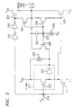
- Fig. 2 shows an illustrative embodiment of the present invention.
- Fig. 3 shows an illustrative resistor used in one embodiment of the invention.
- the present detailed description relates to an improved integrated circuit electrostatic discharge protection technique. It may advantageously be used with output buffers having pull-up and pull-down transistors of a single conductivity type.
- output buffers having pull-up and pull-down transistors of a single conductivity type.
- n-channel output devices are shown.
- a comparable protective circuit for use with p-channel output devices is the same as that shown, except that p-channel transistors are used in lieu of n-channel transistors, and the power supply connections are the opposite of those shown.
- an output conductor (bond pad 200) is connected to n-channel pull-up transistor 201 and n-channel pull-down transistor 202.
- the gates of transistors 201 and 202 are connected to protective transistors 203 and 204, which are also connected to bond pad 200 as shown.
- the gates of protective transistors 203 and 204 are connected to capacitor 205 and resistor 206 at common node 207.
- the high voltage is conducted through capacitor 205 to the gates of transistors 203 and 204. This conduction increases the voltage on the gates of these transistors to approximately the same voltage as on their sources/drain regions also connected to bond pad 200.
- each MOS transistor may be considered to have a bipolar transistor connected in parallel, comprising emitter, base, and collector regions corresponding to the source, channel, and drain regions of the MOS device.
- This conduction through protective transistors 203 and 204 also raises the voltage on the gates of output transistors 201 and 202, respectively. This conduction also lowers the breakdown thresholds of these output transistors, allowing bipolar conduction through these transistors to conduct the ESD current to their respective power supply conductors, V DD and V SS .
- capacitor 205 have a value in the range of from 0.2 to 50 picofarads, and resistor 206 have a value in the range of from 200 ohms to 50 kilohms. Further, I recommend that the RC time constant provided by these devices be preferably in the range of from 1 to 50 nanoseconds. In an illustrative embodiment, capacitor 205 has a nominal value of 3.3 picofarads, whereas resistor 206 has a nominal value of 3 kilohms. These values provide a nominal RC time constant of about 10 nanoseconds.
- the capacitor 205 is illustratively of the MOS type, wherein a conductive polysilicon layer forms a first capacitor plate, and a doped semiconductor substrate (or tub) region forms the second capacitor plate, with a gate-level silicon dioxide layer forming the capacitor dielectric.
- the capacitor may comprise two polysilicon layers for the plates, with a deposited dielectric therebetween. Still other capacitor types are known in the art and may be used.
- resistor 206 is formed in an n-tub in a manner comparable to resistor 209 discussed below. However, it may alternatively be formed in a p-tub, or may be a deposited resistor of the polysilicon or silicide type, or may be of another type known in the art.
- means are also provided for boosting the voltage on the n-tub region in which the p-channel pre-driver transistor is formed during an ESD event.
- This boosting prevents conduction from the drain of the p-channel pre-driver to the underlying n-tub from limiting the voltage on the gate of the associated output transistor during an ESD event. That is, as shown in Fig. 2, the p-type drain of the pre-driver transistor 210 forms a diode 212 with the underlying n-type tub region 213 in which the drain is formed. In prior-art CMOS integrated circuit designs, the tub 213 would be connected directly to the V DD conductor.
- a transistor 208 is connected between the bond pad 200 and the n- tub 213. This transistor 208 also exhibits bipolar breakdown when an ESD event occurs, thereby conducting charge to the n-tub 213 and raising its voltage.
- the n-tub is not connected directly to the V DD conductor, but rather through resistor 209.
- This resistor limits the conduction through diode 212 to the V DD conductor, and hence allows the voltage on the gate of output transistor 202 to rise to a higher level during an ESD event.
- the resistor 209 has a value of about 600 ohms in the exemplary embodiment, and is typically in the range of about 50 to 5000 ohms.
- the resistor may be a deposited (e.g., polysilicon) resistor, or a diffused region in the semiconductor substrate, or other type. For example, as shown in Fig.
- an n-tub 31 may be used to form the resistor 209, which is connected to V DD via n+ contact region 37.
- the resistor is connected via n+ contact region 36, conductor 39, and n+ contact region 35 to the n-tub 30, corresponding to region 213 in Fig. 2.
- the p-channel pre-driver transistor (210 of Fig. 2), comprising source/drain regions 32 and 34, and gate electrode 33, is formed in n-tub 30.
- the p-channel transistor in the pre-driver complementary inverter 214 may be located in an n-tub similarly connected to V DD , or alternatively in the same n-tub as transistor 210.
- tub-boosting transistor 208 and resistor 209 although advantageous in the illustrative embodiment, are not necessary in all cases. That is, the pre-driver stage that produces the logic signal to the output transistor may be of a different design than that shown, and the diode 212 may not be present.
- the pre-driver pull-up device may be an n-channel transistor, rather than a p-channel transistor; hence the source-to-substrate diode would be connected opposite to diode 212 shown, and would not cause clamping of positive voltages.
- the protective transistors 203 and 204 do not carry the actual ESD current themselves.
- the transistors 203 and 204 may be sized to be relatively small, which saves space as compared to certain prior-art techniques.
- the output transistors 201 and 202 that carry the ESD current to one or both of the power supply conductors V SS and V DD .
- the output transistors are usually relatively large anyway, in order to provide sufficient drive capability. Hence, no size increase may be required to provide ESD protection in typical implementations of the present technique.
- the protective transistors 203 and 204 are relatively small, they add minimal capacitive loading to the output circuitry, as compared to the prior-art technique.
- the above embodiment has shown a transistor (e.g., 203 and 204) and an RC network (capacitor 205 and resistor 206) as the protective means that causes the output transistors (201 and 202) to conduct during an ESD event in response to the high voltage on bond pad 200.
- the protective means no longer causes the output transistor to conduct, and they are returned to control by the logic signal from the pre-driver circuitry.
- ESD events occur when the integrated circuit is not connected in a circuit board or multi-chip module, and hence the logic signals are not present anyway. Conversely, when connected in a circuit board or module, the normal operating logic signals may be present, but the ESD events are less likely to occur.
- digital logic circuitry has been discussed herein, the protected circuitry may be analog. Therefore, the desired operational signal (V in ) may be generally referred to as an "information signal".
- the present technique may be used with an output buffer having only a single conductivity type of output transistor.
- CMOS output buffers as well, wherein a p-channel transistor serves as the pull-up device and an n-channel transistor serves as the pull-down device.
- the n-channel pull-down device may still be protected by the circuitry shown in Fig. 2.
- the p-channel device may be protected with comparable circuitry, but with the transistor conductivities opposite to that shown, and also opposite power supply connections.
- a resistor comparable to 209 could then be connected between the p-tub in which the n-channel pre-driver transistor is formed and the V SS power supply conductor.
- the connection between the source/drain electrodes of the output transistors and the output conductor may include a resistor, as shown for example in U. S. patent 4,990,802 coassigned herewith.
Landscapes
- Semiconductor Integrated Circuits (AREA)
- Metal-Oxide And Bipolar Metal-Oxide Semiconductor Integrated Circuits (AREA)
Description
Claims (5)
- An integrated circuit comprising an output transistor (201, 202) having a first controlled electrode connected to a power supply conductor (VDD, VSS), a second controlled electrode connected to an output conductor (200), and a control electrode coupled to receive an information signal (Vin);
wherein said integrated circuit further comprisesa protective field effect transistor (203, 204) having a first source/drain electrode connected to said output conductor, a second source/drain electrode connected to the control electrode of said output transistor, and a gate electrode connected to a first terminal of a capacitor (205) which has a second terminal connected to said output conductor so as to cause said output transistor to conduct during an electrostatic discharge event on said output conductor; anda resistor (206) having a first terminal connected to the gate electrode of said protective transistor and a second terminal connected to a power supply conductor (VSS) so that said protective transistor does not conduct in the absence of an electrostatic discharge event on said output conductor. - An integrated circuit as claimed in claim I wherein said output transistor is an n-channel field effect transistor, said information signal is supplied by a pre-driver stage that comprises a p-channel pull-up transistor (210) that is located in an n-type tub region (213);
and said integrated circuit comprises a field effect transistor (208) for increasing the voltage on said n-type tub region during an electrostatic discharge event and having a first source/drain region connected to said output conductor (200), and a second source/drain region connected to said tub (213). - An integrated circuit as claimed in claim I wherein said output transistor is a p-channel field effect transistor, said information signal is supplied by a pre-driver stage that comprises an n-channel pull-up transistor that is located in an p-type tub region;
and said integrated circuit comprises a field effect transistor for increasing the voltage on said p-type tub region during an electrostatic discharge event and having a first source/drain region connected to said output conductor, and a second source/drain region connected to said tub. - An integrated circuit as claimed in claim 2 comprising a resistor (209) connected between said n-type tub and the positive power supply voltage conductor (VDD).
- An integrated circuit as claimed in claim 1 wherein said protective field effect transistor provides for said output transistor to conduct when the electrostatic discharge event produces a voltage on said output conductor that rises more rapidly than 100 volts per nanosecond.
Applications Claiming Priority (2)
| Application Number | Priority Date | Filing Date | Title |
|---|---|---|---|
| US894405 | 1992-06-05 | ||
| US07/894,405 US5345357A (en) | 1992-06-05 | 1992-06-05 | ESD protection of output buffers |
Publications (2)
| Publication Number | Publication Date |
|---|---|
| EP0575062A1 EP0575062A1 (en) | 1993-12-22 |
| EP0575062B1 true EP0575062B1 (en) | 1998-07-29 |
Family
ID=25403031
Family Applications (1)
| Application Number | Title | Priority Date | Filing Date |
|---|---|---|---|
| EP93304123A Expired - Lifetime EP0575062B1 (en) | 1992-06-05 | 1993-05-27 | ESD protection of output buffers |
Country Status (5)
| Country | Link |
|---|---|
| US (1) | US5345357A (en) |
| EP (1) | EP0575062B1 (en) |
| JP (1) | JP2777047B2 (en) |
| KR (1) | KR0135499B1 (en) |
| DE (1) | DE69319968T2 (en) |
Cited By (1)
| Publication number | Priority date | Publication date | Assignee | Title |
|---|---|---|---|---|
| US6984029B2 (en) | 2003-07-11 | 2006-01-10 | Hewlett-Packard Development Company, Lp. | Print cartridge temperature control |
Families Citing this family (42)
| Publication number | Priority date | Publication date | Assignee | Title |
|---|---|---|---|---|
| US5611053A (en) * | 1994-01-21 | 1997-03-11 | Advanced Micro Devices, Inc. | Apparatus and method for integrating bus master ownership of local bus load by plural data transceivers |
| US6295572B1 (en) * | 1994-01-24 | 2001-09-25 | Advanced Micro Devices, Inc. | Integrated SCSI and ethernet controller on a PCI local bus |
| US5528188A (en) * | 1995-03-13 | 1996-06-18 | International Business Machines Corporation | Electrostatic discharge suppression circuit employing low-voltage triggering silicon-controlled rectifier |
| FR2734674B1 (en) * | 1995-05-24 | 1997-08-14 | Sgs Thomson Microelectronics | CLIPPING DEVICE |
| US5615073A (en) * | 1995-06-22 | 1997-03-25 | National Semiconductor Corporation | Electrostatic discharge protection apparatus |
| US5675469A (en) * | 1995-07-12 | 1997-10-07 | Motorola, Inc. | Integrated circuit with electrostatic discharge (ESD) protection and ESD protection circuit |
| US5631793A (en) * | 1995-09-05 | 1997-05-20 | Winbond Electronics Corporation | Capacitor-couple electrostatic discharge protection circuit |
| US5625280A (en) * | 1995-10-30 | 1997-04-29 | International Business Machines Corp. | Voltage regulator bypass circuit |
| FR2741756B1 (en) * | 1995-11-28 | 1998-01-02 | Sgs Thomson Microelectronics | OVERVOLTAGE PROTECTION CIRCUIT |
| GB2308731A (en) * | 1995-12-22 | 1997-07-02 | Motorola Gmbh | Semiconductor device with electrostatic discharge protection |
| US5771389A (en) * | 1996-02-28 | 1998-06-23 | Intel Corporation | Low slew rate output buffer with staged biasing voltage |
| US6125021A (en) * | 1996-04-30 | 2000-09-26 | Texas Instruments Incorporated | Semiconductor ESD protection circuit |
| US5917689A (en) * | 1996-09-12 | 1999-06-29 | Analog Devices, Inc. | General purpose EOS/ESD protection circuit for bipolar-CMOS and CMOS integrated circuits |
| US5919253A (en) * | 1997-06-25 | 1999-07-06 | Adaptec, Inc. | Hot-switchable SCSI controller having output drivers with quick turn-on |
| JPH1154711A (en) * | 1997-08-04 | 1999-02-26 | Nippon Precision Circuits Kk | Electrostatic protection circuit for semiconductor device |
| US6034552A (en) * | 1998-04-30 | 2000-03-07 | Taiwan Semiconductor Manufacturing Co., Ltd. | Output ESD protection using dynamic-floating-gate arrangement |
| JP2001024496A (en) * | 1999-07-02 | 2001-01-26 | Nec Corp | Input and output circuit |
| WO2001011750A1 (en) * | 1999-08-06 | 2001-02-15 | Sarnoff Corporation | Circuits for dynamic turn off of nmos output drivers during eos/esd stress |
| DE10022366A1 (en) * | 2000-05-08 | 2001-11-29 | Micronas Gmbh | ESD protective structure |
| US6529059B1 (en) | 2000-07-26 | 2003-03-04 | Agere Systems Inc. | Output stage ESD protection for an integrated circuit |
| US6400204B1 (en) | 2000-07-26 | 2002-06-04 | Agere Systems Guardian Corp. | Input stage ESD protection for an integrated circuit |
| FR2813461B1 (en) * | 2000-08-22 | 2003-01-31 | St Microelectronics Sa | PROTECTION DEVICE FOR AN INTEGRATED TRANSISTOR AGAINST ELECTROSTATIC DISCHARGE |
| US6643109B1 (en) * | 2000-09-27 | 2003-11-04 | Conexant Systems, Inc. | Fully synthesisable and highly area efficient very large scale integration (VLSI) electrostatic discharge (ESD) protection circuit |
| US6545520B2 (en) * | 2001-03-28 | 2003-04-08 | Intel Corporation | Method and apparatus for electro-static discharge protection |
| US20030214342A1 (en) * | 2002-05-14 | 2003-11-20 | Darrin Benzer | IO clamping circuit method utilizing output driver transistors |
| US6879476B2 (en) * | 2003-01-22 | 2005-04-12 | Freescale Semiconductor, Inc. | Electrostatic discharge circuit and method therefor |
| US6900970B2 (en) * | 2003-01-22 | 2005-05-31 | Freescale Semiconductor, Inc. | Electrostatic discharge circuit and method therefor |
| JP2005235947A (en) * | 2004-02-18 | 2005-09-02 | Fujitsu Ltd | ESD protection circuit |
| US7573691B2 (en) * | 2004-04-12 | 2009-08-11 | Agere Systems Inc. | Electrical over stress robustness |
| JP4515822B2 (en) * | 2004-05-25 | 2010-08-04 | 株式会社東芝 | Electrostatic protection circuit and semiconductor integrated circuit device using the same |
| US7170324B2 (en) * | 2004-07-15 | 2007-01-30 | Agere Systems Inc. | Output buffer with selectable slew rate |
| JP2006080160A (en) * | 2004-09-07 | 2006-03-23 | Toshiba Corp | ESD protection circuit |
| US7203045B2 (en) * | 2004-10-01 | 2007-04-10 | International Business Machines Corporation | High voltage ESD power clamp |
| US7529070B2 (en) * | 2005-03-11 | 2009-05-05 | Agere Systems Inc. | Power pin to power pin electro-static discharge (ESD) clamp |
| US7692905B2 (en) * | 2006-11-28 | 2010-04-06 | Smartech Worldwide Limited | Electrostatic discharge protection circuit for output buffer |
| US7619862B2 (en) * | 2007-02-22 | 2009-11-17 | Smartech Worldwide Limited | Electrostatic discharge protection circuit for high voltage input pad |
| TW200929783A (en) * | 2007-12-26 | 2009-07-01 | Princeton Technology Corp | ESD protecting leading circuit |
| TW200929768A (en) * | 2007-12-26 | 2009-07-01 | Princeton Technology Corp | ESD protecting circuit with gate voltage raising circuit |
| US9013842B2 (en) * | 2011-01-10 | 2015-04-21 | Infineon Technologies Ag | Semiconductor ESD circuit and method |
| JP5565336B2 (en) * | 2011-02-14 | 2014-08-06 | 富士通セミコンダクター株式会社 | Output circuit, system, and output circuit control method |
| FR3001085A1 (en) * | 2013-01-15 | 2014-07-18 | St Microelectronics Sa | BIDIRECTIONAL SEMICONDUCTOR DEVICE FOR PROTECTION AGAINST ELECTROSTATIC DISCHARGE, USEFUL WITHOUT TRIP CIRCUIT |
| KR102000738B1 (en) | 2013-01-28 | 2019-07-23 | 삼성디스플레이 주식회사 | Circuit for preventing static electricity and display device comprising the same |
Citations (1)
| Publication number | Priority date | Publication date | Assignee | Title |
|---|---|---|---|---|
| EP0523800A1 (en) * | 1991-07-19 | 1993-01-20 | Philips Electronics Uk Limited | An overvoltage protected semiconductor switch |
Family Cites Families (4)
| Publication number | Priority date | Publication date | Assignee | Title |
|---|---|---|---|---|
| US4855620A (en) * | 1987-11-18 | 1989-08-08 | Texas Instruments Incorporated | Output buffer with improved ESD protection |
| JPH01147854A (en) * | 1987-12-04 | 1989-06-09 | Nissan Motor Co Ltd | Semiconductor device |
| US4990802A (en) * | 1988-11-22 | 1991-02-05 | At&T Bell Laboratories | ESD protection for output buffers |
| US5208719A (en) * | 1991-08-20 | 1993-05-04 | Vlsi Technology, Inc. | Output pad electrostatic discharge protection circuit for mos devices |
-
1992
- 1992-06-05 US US07/894,405 patent/US5345357A/en not_active Expired - Lifetime
-
1993
- 1993-05-20 KR KR1019930008622A patent/KR0135499B1/en not_active Expired - Lifetime
- 1993-05-27 DE DE69319968T patent/DE69319968T2/en not_active Expired - Lifetime
- 1993-05-27 EP EP93304123A patent/EP0575062B1/en not_active Expired - Lifetime
- 1993-06-07 JP JP5159948A patent/JP2777047B2/en not_active Expired - Fee Related
Patent Citations (1)
| Publication number | Priority date | Publication date | Assignee | Title |
|---|---|---|---|---|
| EP0523800A1 (en) * | 1991-07-19 | 1993-01-20 | Philips Electronics Uk Limited | An overvoltage protected semiconductor switch |
Cited By (1)
| Publication number | Priority date | Publication date | Assignee | Title |
|---|---|---|---|---|
| US6984029B2 (en) | 2003-07-11 | 2006-01-10 | Hewlett-Packard Development Company, Lp. | Print cartridge temperature control |
Also Published As
| Publication number | Publication date |
|---|---|
| US5345357A (en) | 1994-09-06 |
| DE69319968T2 (en) | 1998-12-24 |
| JP2777047B2 (en) | 1998-07-16 |
| KR0135499B1 (en) | 1998-04-22 |
| DE69319968D1 (en) | 1998-09-03 |
| JPH06163824A (en) | 1994-06-10 |
| HK1003461A1 (en) | 1998-10-30 |
| KR940001389A (en) | 1994-01-11 |
| EP0575062A1 (en) | 1993-12-22 |
Similar Documents
| Publication | Publication Date | Title |
|---|---|---|
| US5345357A (en) | ESD protection of output buffers | |
| US5345356A (en) | ESD protection of output buffers | |
| JP3174636B2 (en) | Electrostatic discharge protection for CMOS integrated circuits | |
| EP0740344B1 (en) | Method and apparatus for coupling multiple independent on-chip Vdd busses to an ESD core clamp | |
| US6040968A (en) | EOS/ESD protection for high density integrated circuits | |
| US5946175A (en) | Secondary ESD/EOS protection circuit | |
| US6867957B1 (en) | Stacked-NMOS-triggered SCR device for ESD-protection | |
| US5959488A (en) | Dual-node capacitor coupled MOSFET for improving ESD performance | |
| US7304827B2 (en) | ESD protection circuits for mixed-voltage buffers | |
| US5502328A (en) | Bipolar ESD protection for integrated circuits | |
| US6756642B2 (en) | Integrated circuit having improved ESD protection | |
| JP3061260B2 (en) | Static electricity protection circuit | |
| US5663678A (en) | ESD protection device | |
| US7907373B2 (en) | Electrostatic discharge circuit | |
| US6337787B2 (en) | Gate-voltage controlled electrostatic discharge protection circuit | |
| US6097235A (en) | Field device electrostatic discharge protective circuit | |
| US6809915B2 (en) | Gate-equivalent-potential circuit and method for I/O ESD protection | |
| US6414360B1 (en) | Method of programmability and an architecture for cold sparing of CMOS arrays | |
| US5349227A (en) | Semiconductor input protective device against external surge voltage | |
| US20030043517A1 (en) | Electro-static discharge protecting circuit | |
| KR100237992B1 (en) | Power sequency independent electrostatic discharge protection circuits | |
| US6181542B1 (en) | Method of making a stack-polysilicon capacitor-coupled dual power supply input/output protection circuit | |
| US5903184A (en) | Semiconductor device having protection circuit | |
| JP2839624B2 (en) | Semiconductor integrated circuit | |
| US20090009917A1 (en) | Electrostatic discharge device |
Legal Events
| Date | Code | Title | Description |
|---|---|---|---|
| PUAI | Public reference made under article 153(3) epc to a published international application that has entered the european phase |
Free format text: ORIGINAL CODE: 0009012 |
|
| AK | Designated contracting states |
Kind code of ref document: A1 Designated state(s): DE FR GB IT |
|
| RAP3 | Party data changed (applicant data changed or rights of an application transferred) |
Owner name: AT&T CORP. |
|
| 17P | Request for examination filed |
Effective date: 19940609 |
|
| 17Q | First examination report despatched |
Effective date: 19960926 |
|
| GRAG | Despatch of communication of intention to grant |
Free format text: ORIGINAL CODE: EPIDOS AGRA |
|
| GRAG | Despatch of communication of intention to grant |
Free format text: ORIGINAL CODE: EPIDOS AGRA |
|
| GRAH | Despatch of communication of intention to grant a patent |
Free format text: ORIGINAL CODE: EPIDOS IGRA |
|
| GRAH | Despatch of communication of intention to grant a patent |
Free format text: ORIGINAL CODE: EPIDOS IGRA |
|
| GRAA | (expected) grant |
Free format text: ORIGINAL CODE: 0009210 |
|
| AK | Designated contracting states |
Kind code of ref document: B1 Designated state(s): DE FR GB IT |
|
| ITF | It: translation for a ep patent filed | ||
| REF | Corresponds to: |
Ref document number: 69319968 Country of ref document: DE Date of ref document: 19980903 |
|
| ET | Fr: translation filed | ||
| PLBE | No opposition filed within time limit |
Free format text: ORIGINAL CODE: 0009261 |
|
| STAA | Information on the status of an ep patent application or granted ep patent |
Free format text: STATUS: NO OPPOSITION FILED WITHIN TIME LIMIT |
|
| 26N | No opposition filed | ||
| PGFP | Annual fee paid to national office [announced via postgrant information from national office to epo] |
Ref country code: GB Payment date: 20010426 Year of fee payment: 9 |
|
| PGFP | Annual fee paid to national office [announced via postgrant information from national office to epo] |
Ref country code: FR Payment date: 20010502 Year of fee payment: 9 |
|
| REG | Reference to a national code |
Ref country code: GB Ref legal event code: IF02 |
|
| PG25 | Lapsed in a contracting state [announced via postgrant information from national office to epo] |
Ref country code: GB Free format text: LAPSE BECAUSE OF NON-PAYMENT OF DUE FEES Effective date: 20020527 |
|
| GBPC | Gb: european patent ceased through non-payment of renewal fee |
Effective date: 20020527 |
|
| PG25 | Lapsed in a contracting state [announced via postgrant information from national office to epo] |
Ref country code: FR Free format text: LAPSE BECAUSE OF NON-PAYMENT OF DUE FEES Effective date: 20030131 |
|
| REG | Reference to a national code |
Ref country code: FR Ref legal event code: ST |
|
| PGFP | Annual fee paid to national office [announced via postgrant information from national office to epo] |
Ref country code: DE Payment date: 20120523 Year of fee payment: 20 |
|
| PGFP | Annual fee paid to national office [announced via postgrant information from national office to epo] |
Ref country code: IT Payment date: 20120518 Year of fee payment: 20 |
|
| REG | Reference to a national code |
Ref country code: DE Ref legal event code: R071 Ref document number: 69319968 Country of ref document: DE |
|
| PG25 | Lapsed in a contracting state [announced via postgrant information from national office to epo] |
Ref country code: DE Free format text: LAPSE BECAUSE OF EXPIRATION OF PROTECTION Effective date: 20130528 |