EP0573821B1 - Display control apparatus and method therefor - Google Patents
Display control apparatus and method therefor Download PDFInfo
- Publication number
- EP0573821B1 EP0573821B1 EP93108083A EP93108083A EP0573821B1 EP 0573821 B1 EP0573821 B1 EP 0573821B1 EP 93108083 A EP93108083 A EP 93108083A EP 93108083 A EP93108083 A EP 93108083A EP 0573821 B1 EP0573821 B1 EP 0573821B1
- Authority
- EP
- European Patent Office
- Prior art keywords
- flag
- display
- data
- address
- window
- Prior art date
- Legal status (The legal status is an assumption and is not a legal conclusion. Google has not performed a legal analysis and makes no representation as to the accuracy of the status listed.)
- Expired - Lifetime
Links
Images






Classifications
-
- G—PHYSICS
- G09—EDUCATION; CRYPTOGRAPHY; DISPLAY; ADVERTISING; SEALS
- G09G—ARRANGEMENTS OR CIRCUITS FOR CONTROL OF INDICATING DEVICES USING STATIC MEANS TO PRESENT VARIABLE INFORMATION
- G09G5/00—Control arrangements or circuits for visual indicators common to cathode-ray tube indicators and other visual indicators
- G09G5/36—Control arrangements or circuits for visual indicators common to cathode-ray tube indicators and other visual indicators characterised by the display of a graphic pattern, e.g. using an all-points-addressable [APA] memory
- G09G5/39—Control of the bit-mapped memory
- G09G5/395—Arrangements specially adapted for transferring the contents of the bit-mapped memory to the screen
-
- G—PHYSICS
- G09—EDUCATION; CRYPTOGRAPHY; DISPLAY; ADVERTISING; SEALS
- G09G—ARRANGEMENTS OR CIRCUITS FOR CONTROL OF INDICATING DEVICES USING STATIC MEANS TO PRESENT VARIABLE INFORMATION
- G09G3/00—Control arrangements or circuits, of interest only in connection with visual indicators other than cathode-ray tubes
- G09G3/20—Control arrangements or circuits, of interest only in connection with visual indicators other than cathode-ray tubes for presentation of an assembly of a number of characters, e.g. a page, by composing the assembly by combination of individual elements arranged in a matrix no fixed position being assigned to or needed to be assigned to the individual characters or partial characters
- G09G3/34—Control arrangements or circuits, of interest only in connection with visual indicators other than cathode-ray tubes for presentation of an assembly of a number of characters, e.g. a page, by composing the assembly by combination of individual elements arranged in a matrix no fixed position being assigned to or needed to be assigned to the individual characters or partial characters by control of light from an independent source
- G09G3/36—Control arrangements or circuits, of interest only in connection with visual indicators other than cathode-ray tubes for presentation of an assembly of a number of characters, e.g. a page, by composing the assembly by combination of individual elements arranged in a matrix no fixed position being assigned to or needed to be assigned to the individual characters or partial characters by control of light from an independent source using liquid crystals
- G09G3/3611—Control of matrices with row and column drivers
- G09G3/3622—Control of matrices with row and column drivers using a passive matrix
- G09G3/3629—Control of matrices with row and column drivers using a passive matrix using liquid crystals having memory effects, e.g. ferroelectric liquid crystals
-
- G—PHYSICS
- G09—EDUCATION; CRYPTOGRAPHY; DISPLAY; ADVERTISING; SEALS
- G09G—ARRANGEMENTS OR CIRCUITS FOR CONTROL OF INDICATING DEVICES USING STATIC MEANS TO PRESENT VARIABLE INFORMATION
- G09G3/00—Control arrangements or circuits, of interest only in connection with visual indicators other than cathode-ray tubes
- G09G3/20—Control arrangements or circuits, of interest only in connection with visual indicators other than cathode-ray tubes for presentation of an assembly of a number of characters, e.g. a page, by composing the assembly by combination of individual elements arranged in a matrix no fixed position being assigned to or needed to be assigned to the individual characters or partial characters
- G09G3/34—Control arrangements or circuits, of interest only in connection with visual indicators other than cathode-ray tubes for presentation of an assembly of a number of characters, e.g. a page, by composing the assembly by combination of individual elements arranged in a matrix no fixed position being assigned to or needed to be assigned to the individual characters or partial characters by control of light from an independent source
- G09G3/36—Control arrangements or circuits, of interest only in connection with visual indicators other than cathode-ray tubes for presentation of an assembly of a number of characters, e.g. a page, by composing the assembly by combination of individual elements arranged in a matrix no fixed position being assigned to or needed to be assigned to the individual characters or partial characters by control of light from an independent source using liquid crystals
- G09G3/3611—Control of matrices with row and column drivers
- G09G3/3648—Control of matrices with row and column drivers using an active matrix
- G09G3/3651—Control of matrices with row and column drivers using an active matrix using multistable liquid crystals, e.g. ferroelectric liquid crystals
-
- G—PHYSICS
- G09—EDUCATION; CRYPTOGRAPHY; DISPLAY; ADVERTISING; SEALS
- G09G—ARRANGEMENTS OR CIRCUITS FOR CONTROL OF INDICATING DEVICES USING STATIC MEANS TO PRESENT VARIABLE INFORMATION
- G09G2310/00—Command of the display device
- G09G2310/04—Partial updating of the display screen
-
- G—PHYSICS
- G09—EDUCATION; CRYPTOGRAPHY; DISPLAY; ADVERTISING; SEALS
- G09G—ARRANGEMENTS OR CIRCUITS FOR CONTROL OF INDICATING DEVICES USING STATIC MEANS TO PRESENT VARIABLE INFORMATION
- G09G5/00—Control arrangements or circuits for visual indicators common to cathode-ray tube indicators and other visual indicators
- G09G5/14—Display of multiple viewports
Definitions
- the present invention relates to a display control apparatus and a method therefor and, more particularly, to a display control apparatus and a method therefor, suitable for a display device having a display element having, e.g., a ferroelectric liquid crystal as an operation medium for updating a display state so as to be able to hold the updated display state upon application of an electric field.
- a display element having, e.g., a ferroelectric liquid crystal as an operation medium for updating a display state so as to be able to hold the updated display state upon application of an electric field.
- a display device is generally used in an information processing system or the like, as an information display means having a function of visually expressing information.
- a CRT display device is most popular as such a display device.
- a CRT has a large volume because a considerably large length is required in the direction of thickness of the display screen.
- a compact display device cannot be obtained as a whole. Degrees of freedom in use of an information processing system having a CRT as a display device, i.e., degrees of freedom in installation locations and portability are limited.
- a liquid crystal display device (to be referred to as an LCD hereinafter) can be used. That is, according to the LCD, the display device can be made compact (particularly low profile) as a whole.
- a display (to be referred to as an FLCD or FLC display hereinafter) using a liquid crystal cell containing a ferroelectric liquid crystal (to be referred to as an FLC hereinafter) is included in such LCDs.
- One of the characteristic features of the FLCD lies in that the liquid crystal cell has a storage characteristic of a display state upon application of an electric field.
- the FLCD has the liquid crystal cell having a sufficiently small thickness, FLC molecules are aligned in a first or second stable state in accordance with the direction of electric field application, and this aligned state is maintained after the electric field is removed.
- the FLCD has a storage characteristic by the bistable properties of the FLC molecules. The details of the FLC and FLCD are described in, e.g., Japanese Patent Application No. 62-76357 (U.S. Patent Application S.N. 174,980 filed on March 29, 1988).
- the FLCD can be driven to obtain a sufficient time margin in a continuous refresh driving cycle of the display screen.
- partial rewrite driving for updating the display state of only a portion subjected to updating on the display screen can be performed.
- an FLC display updating time is relatively long.
- the FLCD cannot often cope with a change in display information (e.g., a cursor, a character input, and scrolling), the display state of which must be immediately updated. Therefore, partial rewrite driving as one of the characteristic features of the FLCD is performed to increase an apparent display speed.
- a conventional partial rewrite technique is to store all lines having the updated display contents and rewrite all the lines having the updated display contents by partial rewrite operations. For this reason, independent jobs are to be performed on a plurality of windows as in a multiwindow system, the following problem is posed. For example, when character scrolling is being performed in a window different from a current window (to be referred to as an active window hereinafter), a partial rewrite operation is performed in both the active window and the window subjected to scrolling to result in a decrease in display content rewrite speed. Therefore, partial rewrite operations cannot be sufficiently enhanced.
- EP-A-0 318 050 For an example of the prior art see EP-A-0 318 050.
- a host device such as a CPU
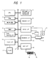
- Fig. 1 is a block diagram of an information processing system incorporating a display control apparatus according to an embodiment of the present invention.
- the information processing system includes a CPU 1, a system bus 2, an arithmetic operation processor 3, a ROM 4, a main memory 5, a DMA (Direct Memory Access) controller (to be referred to as a DMAC hereinafter) 6, an interrupt (INTR) controller 7, an RS232C interface (I/F) 8, a disc I/F 9, a hard disc drive 10, a floppy disc drive 11, a printer I/F 12, a printer 13, a keyboard 14, a mouse 15, a key I/F 16, an FLCD (FLC display) 17, and an FLCD I/F 18.
- the CPU 1 controls the overall operation of the information processing system.
- the system bus 2 comprises an address bus, a control bus, and a data bus.
- the arithmetic operation processor 3 exclusively performs arithmetic operations.
- the ROM 4 stores programs for initializing the entire system.
- the main memory 5 stores programs and is used as a work area.
- the DMAC 6 directly exchanges data with I/Os without being through the CPU 1.
- the interrupt controller controls an interrupt between the CPU 1 and I/Os when an interrupt request is input from an I/O device.
- the RS232C I/F 8 performs communication through a modem using a public or leased line.
- the disc I/F 9 interfaces the hard disc drive 10 and the floppy disc drive 11.
- the printer 13 is represented by an impact printer and a non-impact printer such as a laser beam printer or an ink-jet printer.
- the printer I/F 13 interfaces the printer 12.
- the keyboard 14 is used to enter characters such as letters and numerical values and other inputs.
- the mouse 15 serves as a pointing device.
- the key I/F 16 interfaces the keyboard 14 and the mouse 15.
- the FLCD 17 can be arranged using a display disclosed in Japanese Laid-Open Patent Application No. 63-243993 filed by the present applicant.
- the FLCD I/F 18 interfaces the FLCD 17.
- a general system user performs operations in correspondence with various kinds of information displayed on the display screen of the FLCD 17. More specifically, image information and the like from the RS232C I/F 8, the hard disc drive 10, the floppy disc drive 14, and the mouse 15 or operation information and the like representing user's system operations and read out from the ROM 4 and the main memory 5 are displayed on the display screen of the FLCD 17, and the user watches the display contents to edit information and designate system inputs.
- the respective components described above constitute display information supply means for the FLCD 17.
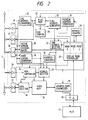
- Fig. 2 is a block diagram showing an arrangement of the FLCD I/F 18 as an embodiment of the display control apparatus according to the present invention.
- the FLCD I/F 18 includes an address bus driver 19, a control bus driver 20, and data bus drivers 21, 36, and 37.
- An address from the CPU 1 is supplied to a line address converter 22, an address selector 23, an active window discriminator 38, and a hard cursor generator 39 through the address bus driver 19.
- a control signal from the CPU 1 is supplied to a memory controller 24 through the control bus driver 20.
- the memory controller 24 generates a control signal for the address selector 23, a control signal for a data selector 40, and a control signal for a video memory 25 (to be described in detail later).
- the address selector 23 selects one of the three addresses supplied to an input section of the address selector 23 on the basis of the control signal from the memory controller 24 and supplies the selected address to the video memory 25.
- the hard cursor generator 39 generates a cursor on the display screen of the FLCD 17 at a position pointed with the mouse 15 serving as the pointing device. Cursor position data is input from the CPU 1 to the hard cursor generator 39 through the data bus driver 36, the hard cursor generator 39 supplies data representing a cursor shape such as an arrow to the data selector 40. At the same time, the hard cursor generator 39 supplies the address for the video memory 25 to the address selector 23 an the line address converter 22. The memory controller 24 switches between the address selector 23 and the data selector 40 in accordance with the control signal from the hard cursor generator 39, thereby selectively supplying the signal from the hard cursor generator 39 to the video memory 25.
- the video memory 25 stores display data, comprises a dual-port DRAM (dynamic RAM), and reads out or writes data through the data bus driver 21.
- the display data written in the data bus driver 21 is transferred to the FLCD 17 through a driver receiver 26 and is displayed on the FLCD 17.
- the driver receiver 26 supplies a sync signal from the FLCD 17 to a display mode controller 27.
- the display mode controller 27 determines the number of partial rewrite operations in accordance with information from a flag counter 28 every time a total refresh operation of one frame is completed.
- the total refresh operation is to update the entire display screen in a predetermined order. Data is read out from the video memory 25 in this order and is transferred to the FLCD 17.
- a partial rewrite operation is to preferentially update the display content of a portion, the display content of which is updated by the CPU.
- the partial rewrite operation is an interrupt operation between frames refreshed in the predetermined order. A relationship between the total refresh and partial rewrite operations will be described in detail later.
- the display mode controller 27 supplies a control signal to a refresh counter 29 to increments the count.
- a counter value from the refresh counter 29 is supplied to a refresh address generator 30 and is converted into a line address for actually refreshing the frame (screen).
- the line address is input to one input section of a line address counter 31.
- the line address counter 31 selects and outputs the line address from the refresh address generator 30 in accordance with the control signal from the display mode controller 27.
- the refresh counter 29 performs a count-up operation by one frame, the refresh counter 29 informs this to the display mode controller 27.
- the display mode controller 27 determines the number of partial rewrite operations in accordance with a mode selected by the information from the active window discriminator 38 upon reception of this information with reference to the counter value from the flag counter 28. Alternatively, every time a partial rewrite operation is executed, the counter value from the flag counter 28 is referred to execute partial rewrite operations a predetermined number of times; or when the counter value becomes "0", a total refresh operation of one frame is executed.
- the line address converter 22 detects write access in the display area from all the kinds of access.
- the line address converter 22 converts an address into a display line address which is then supplied to the flag memory 32.
- the flag memory 32 has a storage capacity corresponding to the display line address and represents a flag for determining whether this line address represents a line candidate to be partially rewritten and displayed. For example, in the flag memory 32, a storage location corresponding to the write access in the display area, i.e., the line address corresponding to the change in display content is set at "1". This indicates a partial rewrite candidate.
- the flag memory 32 monitors a line address from the line address 31 to set a storage location corresponding to the line address output to the FLCD 17 to "0". This indicates that a total refresh or partial rewrite operation is performed to output the line address to the FLCD 17 to change the display state. In other words, this indicates that the candidate is not the partial rewrite candidate. In this manner, in the flag memory 32, a flag is set at the line address corresponding to the data write access. When data of this line is output, the flag is reset.
- the flag counter 28 when the flag is set (i.e., a change from 0 to 1) in the flag memory 32, the flag counter 28 performs a count-up operation; and when the flag is reset (i.e., a change from 1 to 0) in the flag memory 32, the flag counter 28 performs a count-down operation, thereby representing the number of flags set in the flag memory 32. Any other means may be proposed. However, to cause the flag counter 28 to count the number of flags set in the flag memory 32 is to indicate a necessary degree of partial rewriting. The output from the flag counter 28 is supplied to the display mode controller 27.
- a flag address generator 33 refers to the flag memory 32 to detect the set flag, i.e., determine the line address subjected to the partial rewrite operation, and supplies the detection result to one input section of the line address selector 31. To perform a partial rewrite operation, the line address connected to the flag address generator 33 in the line address selector 31 is selected and output under the control of the display mode controller 27.
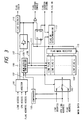
- a selector 103 in the flag memory 32 receives a line address from the line address selector 31, which address is output to the FLCD 17, CPU line addresses as a write address from the CPU 1 and a write address from the hard cursor generator 39, and a flag address from the flag address generator 33.
- An arbiter 101 arbitrates these three kinds of access operations.
- An access kind signal 102 as the result of arbitration is applied to the selector 103.
- An output from the selector 103 is applied as a flag memory address of a memory 104.
- a priority order is determined in an order of CPU access (VRAM rewrite cycle), line access (refresh cycle), and flag address cycle (partial rewrite cycle), and access timings of the flag memory 32 are shown in Fig. 4.
- a CPU line address is selected by the selector 103 and is applied to the memory 104.
- a line subjected to rewriting is detected by a memory access controller 106 in accordance with the access kind signal 102 and a comparison result from a comparator 105 for comparing the CPU line address and the line address. That is, first of all, the flag is loaded (flag memory read data) and is then read out, and flag data which determines a CPU/line signal 107 is written in the memory 104 (flag memory write data).
- the CPU/line signal 107 is determined by the arbiter 101 in accordance with whether the access is CPU access or line access.
- the CPU/line signal 107 is gated and output in accordance with a flag write signal from the memory access controller 106, thereby obtaining flag data.
- the line address is selected by the selector 103 and is applied to the memory 104.
- the same operation as in CPU access is performed.
- the line access is different from the CPU access in that flag corresponding to the line output to the FLCD 17 is reset ("0").
- the CPU line address does not coincide with the line address, the CPU access is preferentially performed to process the flag, and the flag corresponding to the line access is then processed, as indicated in the access state of CPU ⁇ line is the timings of Fig. 4.
- the flag processing operations in the CPU access and line access are the same as those in either CPU access or line access. As described above, the flag is preferentially set in CPU access, and the order of line access is lowered to reset the flag. When CPU access contends with line access, a flag is always set for CPU access to properly reset the flag for the line output to the FLCD 17.
- flag address access a flag address is selected by the selector 103 and is applied to the memory 104.
- the memory access controller 106 controls to only load the flag in the memory 104 but not to write data in the memory 104.
- flag access flag processing is finally performed, as indicated by the access conditions of CPU ⁇ line and the flag.
- the flag counter 28 is constituted by a general up/down counter, monitors updating of data supplied to the flag memory 32, and counts the number of flags stored in the flag memory 32.
- the memory access controller 106 reads out the flag from the memory 104 from the beginning, and the readout flag data is latched by a D-FF in response to a flag read signal 111.
- a negative logic output of the latch data is supplied as an up/down signal for the flag counter 28.
- the latch data and the flag data are exclusively logically ORed to discriminate a coincidence or noncoincidence. If the coincidence is established, the flag data is not updated, and the flag counter is not operated. However, when the noncoincidence is established, since the flag data has been updated, the flag counter is operated.
- a negative logic signal of the exclusive OR signal is output as a flag counter enable signal.
- a flag mask register 113 is a register used when a partial rewrite operation is performed in a specific area such as a window on the display screen.
- the flag mask register 113 has a one-bit capacity corresponding to the line flag in the memory 104.
- Start coordinate data in Fig. 18 represents the upper left coordinate point of the corresponding window
- X size data represents the size of the corresponding window in the direction of height
- Y size data represents the size of the corresponding window in the direction of width.
- An active flag is a flag representing that the corresponding window is selected as a real working area. These data are set in registers open for each window. Of these data, the address line of the window can be calculated in accordance with the start coordinate data and the X size data. For example, "1" is set in the flag mask register 113 for a line flag to be masked, and "0" is set in the flag mask register 113 corresponding to the line flag subjected to partial rewriting. When output data and the line flag of the memory 104 are logically ANDed, the line flag can be masked.
- the active window discriminator 38 generates a mode select signal for selecting one of the plurality of modes in the display mode controller 27 (to be described later). In this embodiment, one of the three modes is selected.
- the number of address lines which serves as a threshold value for mode selection is set in a size register 121 in advance. When no window is open and an active flag is not set in the window register 120, a signal line 124 is set at "1".
- the X size data of each window corresponding to the set active flag and a value (to be referred to as S hereinafter) set in the size register 121 are compared in a comparator 122. If the X size data is S or less, a signal line 125 is set at "1". However, when the X size data is larger than S, a signal line 156 is set at "1". This result is encoded by an encoder 123, and the encoded signal is input to the display mode controller 27.
- only one size register 121 is used to set the threshold value.
- a plurality of size registers 121 are arranged to increase the number of modes in the display mode controller 27, thereby obtaining display states finely corresponding to sizes of the windows.
- Fig. 6 shows an arrangement for realizing the display mode controller 27.
- a frame end is a signal for causing the refresh counter 29 to signal the end of frame.
- HSYNC is a data request signal from the FLCD 17.
- a flag counter value is a counter value from the flag counter 28.
- a mode select signal is input to the active window discriminator 38 and decoded by a decoder 133. The decoded signal selects one of a mode 0 table 130, a mode 1 table 131, and a mode 2 table 132.
- the mode 0 table 130, the mode 1 table 131, and the mode 2 table 132 are shown in Fig. 19.
- a flag counter value is converted into the corresponding number of partial rewrite operations by the mode 0 table 130, the mode 1 table 131, or the mode 2 table 132. For example, when no window is open, the mode 0 table 130 is selected. If the flag counter value is "0", any partial rewrite operation need not be performed, and the partial rewrite operation is not performed. When the flag counter value is a value falling within the range of 1 to 50, the number of partial rewrite operations is determined in proportion to the flag counter value, and partial rewrite operations of all the lines requiring partial rewriting are performed. The rewritten lines are then output. When the flag counter value is 51 or more, the number of partial rewrite operations is increased, and a refresh rate becomes low.
- the maximum number of partial rewrite operations is limited to 20.
- all the rewritten lines are defined as partial rewrite objects.
- partial rewriting is performed in accordance with the value of the size register 121 in which the number of lines subjected to partial rewrite operations is preset as in the mode 2. With this control, the partial rewrite function as the feature of the FLC is effectively utilized to obtain high-quality display contents.
- a timing circuit 134 determines the end of frame or a display mode every HSYNC.
- the timing circuit 134 sets the partial rewrite mode of a refresh/partial rewrite signal.
- the timing circuit 134 supplies a load signal to a counter 135 to load the number of partial rewrite operations from the mode 0 table 130, the mode 1 table 131, or the mode 2 table 132.
- the counter is operated every HSYNC.
- the refresh/partial rewrite signal is set to the refresh mode. Thereafter, this state is continued until the end of refreshing of one frame.
- a refresh interlace mode may be changed depending on a flag counter value.
- a signal representing a change in refresh interlace mode is sent from the mode 0 table 130, the mode 1 table 131, or the mode 2 table 132 to the timing circuit 134.
- An interlace mode designation signal is output from the timing circuit 134.
- a total refresh method may be a non-interlace method for continuously updating lines from the uppermost line downward, a two-line interlace method for interlacing every other line as in a CRT or the like, or a random interlace method unique to the FLCD 17.
- the random interlace method is used to suppress screen flickering, or the noninterlace method is used to continuously update the screen. In this manner, the different interlace methods are selectively used.
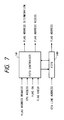
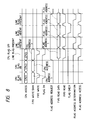
- FIG. 7 An arrangement of a FIFO flag address generator used as the flag address generator 33 is shown in Fig. 7. Timings of the flag address generator shown in Fig. 7 is shown in Fig. 8.
- Input data to a FIFO 140 is a CPU line address (FIFO write data) supplied through the line address converter 22, and an output from the FIFO 140 is a flag address (FIFO read data) supplied to the line address selector 31.
- the CPU line address is input to the FIFO 140 in accordance with the FIFO write signal under the control of a FIFO controller 141.
- a flag ON discriminator 112 in the flag memory 32 In order to prevent the CPU line address from being input to the FIFO 140 in an overlap manner, a flag ON discriminator 112 in the flag memory 32 generates a flag ON signal in accordance with the access kind signal 102 from the arbiter 101 and the up/down signal.
- the flag ON signal is set at "1" when the flag is set.
- the flag ON signal When the flag is reset, the flag ON signal is set at "0".
- the FIFO controller 141 does not input the corresponding line address to the FIFO 140 because this line address has already been input in the FIFO 140.
- the FIFO controller 141 inputs the line address to the FIFO 140 because this line address is not yet input to the FIFO 140.
- the FIFO controller 141 sequentially generates the line addresses stored in the FIFO 140 as flag addresses in accordance with the FIFO read signal.
- a flag address access signal is simultaneously generated by the FIFO controller 141. This flag address access signal is used to arbitrate access in the arbiter 101 in the flag memory 32. When flag address access obtains an access right, a flag address is applied to the memory 104.
- a flag check circuit 110 generates a flag check signal on the basis of a flag address cycle signal 109 from the arbiter 101 and the readout flag data to discriminate whether a flag is present.
- the flag check signal is set at "0".
- the flag check signal is set at "1".
- the FIFO controller 141 discriminates that the line address stored in the FIFO 140 is already output, and a flag address is read out from the FIFO 140 again. If the flag check signal is set at "1", the FIFO controller 141 discriminates that the line address is not yet output.
- the FIFO controller 141 outputs the flag address and a flag address determination signal.
- the display mode controller 27 switches the line address selector 31 to output a flag address as a line address.
- Line addresses output from the line address selector 31 by total refresh and partial rewrite operations are input to an address converter 34, an address/data synthesizer 35, and the flag memory 32.
- the address converter 34 converts a display line address into an address for the DRAM in the video memory 25.
- the converted address is selected and output by the address selector 23 in accordance with a data transfer request from the display mode controller 27 to the memory controller 24. At this time, a data transfer cycle is generated by the memory controller 24 in the video memory 25. Data corresponding to the address selected and output by the address selector 23 is read out from the DRAM and is supplied to the address/data synthesizer 35.
- the address/data synthesizer 35 synthesizes the line address from the line address selector 31 and the data from the video memory 25, and the synthesized data is transferred to the FLCD 17 through the driver receiver 26. The data is then displayed on the FLCD 17.
- the FLCD 17 has a display screen 150, a cursor 151 has a shape of an arrow.
- the display screen 150 has a first open window 152 and a next open window 153.
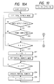
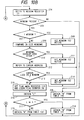
- Figs. 10A and 10B are flow charts showing a flow for executing total refresh and partial rewrite operations.
- a total refresh mode is set in step 201.
- start of data supply to the FLCD 17 is confirmed in step 202, the flow advances to step 203 to wait until a total refresh operation of one frame is executed.
- the window register 120 is referred to in step 204 to discriminate whether a window is open. The subsequent control branches into stage 1 to stage 5, so that control of each stage until the flow advances to step 221 will be described below.
- Step 1 Since no window is open at this moment, the flow advances to step 206, and a number N of partial rewrite operations is obtained from the flag counter value from the mode 0 table 130 in the display mode controller 27. The flow then advances to step 220.
- step 215 to refer to the line address of the active window and set the flag mask register 113 in the flag memory 32 so as to mask lines except for the line corresponding the referred line address.
- the flag counter 28 is cleared. Only the active window is subjected to partial rewriting.
- step 216 the number L of lines of the active window is calculated.
- step 217 the calculated value is compared with the size value S preset in the size register 121 in the active window controller 38 to discriminate whether the mode 1 table 131 or the mode 2 table 132 in the display mode controller 27 is referred to.
- L is smaller than S, and the flow advances to step 218.
- step 218 the number N of partial rewrite operations is obtained from the mode 1 table 131 in accordance with a flag counter value, and the flow advances to step 220.
- step 3 Since the two windows are open, the flow advances from step 207 to step 209. A degree of overlapping of the windows is calculated by software processing using the data from the window register 120. If the two windows are discriminated to overlap each other in step 210, the flow advances to step 211. Otherwise, the flow advances to step 212. In stage 3, since the two windows overlap each other, the flow advances to step 211, and "1" is set in the active bit corresponding to the window 153 in the window register 120. The flow advances to step 215 to refer to a line address of an active window from the window register 120, and the flag mask register 113 is set in the flag memory 32 so that line flags except for the line flag corresponding to the line address of the active window are masked.
- step 216 The number N of the active window 216 is calculated in step 216.
- step 217 the calculated value is compared with the size value S preset in the size register 121. In this case, L is larger than S, and the flow advances to step 219.
- step 219 the number N of partial rewrite operation is obtained from the mode 2 table 132 in accordance with the flag counter value.
- step 4 Since the two windows are open, the flow advances from step 207 to step 209. In this case, these windows do not overlap each other, and the flow advances from step 210 to step 212. Cursor address information from the hard cursor generator 39 is referred to in step 213 to discriminate that the cursor is present in one of the windows. If YES in step 213, the flow advances to step 214. Otherwise, the flow advances to step 215. In stage 4, since the cursor is not located within any window, setup of the active window is not changed, and the flow advances to step 215.
- a line address of an active window from the window register 120 is referred to, and the flag register 113 in the flag memory 32 is set such that line flags except for the line flag corresponding to the line address of the active window are masked.
- the flag counter 28 is cleared.
- step 216 the number L of lines of the active window is calculated.
- step 217 the calculated value is compared with the size value S preset in the size register 121. In this case, the size of the active matrix does not change from that in stage 3, and the flow advances to step 219. If the size of the active window changes, and L is smaller than S, the flow advances to step 218.
- the number N of partial rewrite operations is obtained from the mode 2 table 132 in accordance with the flag counter value, and the flow advances to step 221.
- step 5 Since the two windows are open, the flow advances from step 207 to step 209. In addition, these windows do not overlap each other, so that the flow advances from step 210 to step 212.
- step 212 cursor address information from the hard cursor generator 39 is referred to.
- step S213 since the cursor is present in the window 132, the flow advances to step 214.
- the window 152 is set as an active window, and "1" is set in the active bit corresponding to the window 152 in the window register 120.
- step 215 sets the flag mask register 113 in the flag memory 32 so that line flags except for the line flag corresponding to the line address of the active window are masked. At the same time, the flag counter 28 is cleared.
- step 216 the number L of lines of the active window is calculated.
- step 217 the calculated value is compared with the size value S preset in the size register 121. In this case, L is smaller than S, and the flow advances to step 218.
- two windows are open.
- a description will be similarly made when three or more windows are open. That is, the number of windows is not limited to two.
- step 220 the number N of partial rewrite operations is discriminated to be "0" or not. If not "0" in step 220, N-1 is substituted in a control variable n . This operation corresponds to loading in the counter 135.
- step 225 n-1 is substituted into n , and the flow advances to step 223. When it is discriminated that the partial rewrite operations are completed by the preset number of times, the flow returns to the first step 201 to set a total refresh mode again and wait for the next output.
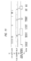
- Fig. 11 shows the relationship between the total refresh and partial rewrite operations.
- CPU write data 41 is written by the CPU 1 in a display region of the video memory 25 through the address driver 19.
- Data updating is frequently performed in an area where lines are dense.
- a change in display content is less frequent in an area where lines are sparse.
- a flag counter value 42 is a value represented by the flag counter 28.
- the flag counter line 42 represents the number of updated lines. Even if the counter is counted up by the CPU write data 41, the counter counts down a total refresh output. For this reason, the flag counter value 42 at the end of total refresh mode of one frame represents the number of lines rewritten by the CPU 1 after the total refresh data of this frame are output.
- a total refresh/partial rewrite signal 43 is set at "1" for the total refresh cycle and "0" for the partial rewrite cycle.
- the means for calculating and setting data in the flag mask register 113 in the flag memory 32 in a software manner using the start coordinate data (X) and the X size data set in the window register 120 in the active window discriminator 38 has been described.
- a means for obtaining data set in a flag mask data 113 by a hardware circuit will be described below.
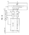
- Fig. 12 is a detailed block diagram showing the arrangement of an FLCD I/F 18 of this embodiment.
- the same reference numerals as in Fig. 1 denote the same parts, and a detailed description thereof will be omitted.
- a window size discriminator 45 is a circuit for calculating a line address of an active window in this embodiment.
- Fig. 13 is a block diagram showing an arrangement of the window size discriminator 45.
- a mask flag controller 160 discriminates whether an active flag is set. If so, start coordinate data (X) and X size data of this attribute are latched in an attribute memory circuit 161. At the same time, "1" is set in a mask flag 164, and data is set so as to mask all the line flags.
- the start coordinate data (X) latched by the attribute memory circuit 161 is decoded by a decoder 162 to obtain a start address for canceling the mask data in the mask flag 164.
- the X size data latched by the attribute memory circuit 161 is loaded in a counter 163 to set mask flags 164 corresponding to the value of the counter 164 from the start address to be zero, thereby preventing the line flag from being masked.
- the value of the mask flag 164 is input to the flag mask register 113.
- the line address of the active window is calculated by the hard circuit, as described above.
- the window attribute is input to the window register 120 in the active window discriminator 38, the value of the flag mask register 113 is automatically set without using software.
- the first embodiment exemplifies the means for calculating and setting data representing whether windows overlap each other in accordance with software using the start coordinate data, the X size data, and the Y size data, all of which are set in the window register 120 in the active window discriminator 38, when a plurality of windows are open.
- a means for detecting overlapping of windows by a hard circuit having flags corresponding to the size of the display screen will be described.
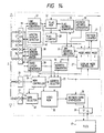
- Fig. 14 is a detailed block diagram showing the arrangement of an FLCD I/F 18 of this embodiment.
- the same reference numerals as in Fig. 1 denote the same parts in Fig. 14, and a detailed description thereof will be omitted.
- a window overlap detector 46 is a circuit for detecting overlapping of windows in this embodiment.
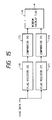
- Fig. 15 is a block diagram showing an arrangement of the window overlap detector 46.
- the window overlap detector 46 comprises a flag register (X) 170 corresponding to the display lines in the vertical (X) direction of an FLCD 17, and a flag register (Y) 171 corresponding to the display lines in the horizontal (Y) direction of the FLCD 17.
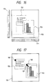
- FIG. 16 A correspondence between the display screen of the FLCD 17 and the flag registers (X) 170 and (Y) 171 is shown in Fig. 16.
- a window is open on the display screen of the FLCD 17
- line addresses of the open window in the X and Y directions are obtained from a window register 120, and "1"s are respectively set in the flag registers (X) 170 and (Y) 171.
- the contents of the flag registers (X) 170 and (Y) 171 which correspond to the previously open window are saved in comparators (X) 172 and (Y) 173.
- the flag registers (X) 170 and (Y) 171 corresponding to the X and Y directions of the newly open window are set at "1".
- a window overlap flag 174 is set.
- a CPU 1 can refer to the window overlap flag 174 through a data bus driver 47 to detect whether the windows overlap each other.
- the means for discriminating the active window comprises the means for calculating a cursor position and detecting a window in which the cursor is present when a plurality of windows are open and these windows are displayed on the display screen.
- a means for causing a user of this system to arbitrarily select an active window will be described.
- Fig. 17 shows a display screen state of an FLCD 17 of this embodiment.
- the same reference numerals as in Fig. 9 denote the same parts in Fig. 17.
- Fig. 17 shows the state in which two windows are displayed on the display screen.
- each active area 180 is an area for setting an active window.
- the active flag of the attribute data corresponding to the corresponding window input in a window register 120 is set, and the window having the clicked active area 180 is defined as an active window subjected to partial rewriting.
- two windows are open.
- the same control as described above can be performed even if three or more windows are open.
- the means for discriminating the active window is not limited to the one exemplified in this embodiment.
- An active window may be discriminated by a means employed by application software.
- the active area 180 is formed to designate the active area.
- a cursor may be placed in a window and is clicked to set this window as an active window.
- the active window is discriminated in accordance with the coordinate position, size, and height of the window and the cursor position.
- a means for executing a cycle for updating the display of a portion whose display contents are changed by a host device such as a CPU is arranged.
- a means for representing that the portion whose display contents are changed is not updated on the display screen is arranged.
- a means for executing the cycle for updating the display of the portion whose display contents are changed from the host device such as the CPU within a specified range is arranged.
- a means for determining the number of cycles for updating the display of the portion, whose display contents are changed, in accordance with the number of portions whose display is not updated, among the portions whose display contents are changed, is also arranged.
Landscapes
- Engineering & Computer Science (AREA)
- Physics & Mathematics (AREA)
- Computer Hardware Design (AREA)
- General Physics & Mathematics (AREA)
- Theoretical Computer Science (AREA)
- Chemical & Material Sciences (AREA)
- Crystallography & Structural Chemistry (AREA)
- Liquid Crystal Display Device Control (AREA)
- Liquid Crystal (AREA)
Description
- The present invention relates to a display control apparatus and a method therefor and, more particularly, to a display control apparatus and a method therefor, suitable for a display device having a display element having, e.g., a ferroelectric liquid crystal as an operation medium for updating a display state so as to be able to hold the updated display state upon application of an electric field.
- A display device is generally used in an information processing system or the like, as an information display means having a function of visually expressing information. A CRT display device is most popular as such a display device. A CRT has a large volume because a considerably large length is required in the direction of thickness of the display screen. A compact display device cannot be obtained as a whole. Degrees of freedom in use of an information processing system having a CRT as a display device, i.e., degrees of freedom in installation locations and portability are limited.
- To compensate for these drawbacks, a liquid crystal display device (to be referred to as an LCD hereinafter) can be used. That is, according to the LCD, the display device can be made compact (particularly low profile) as a whole. A display (to be referred to as an FLCD or FLC display hereinafter) using a liquid crystal cell containing a ferroelectric liquid crystal (to be referred to as an FLC hereinafter) is included in such LCDs. One of the characteristic features of the FLCD lies in that the liquid crystal cell has a storage characteristic of a display state upon application of an electric field. More specifically, the FLCD has the liquid crystal cell having a sufficiently small thickness, FLC molecules are aligned in a first or second stable state in accordance with the direction of electric field application, and this aligned state is maintained after the electric field is removed. The FLCD has a storage characteristic by the bistable properties of the FLC molecules. The details of the FLC and FLCD are described in, e.g., Japanese Patent Application No. 62-76357 (U.S. Patent Application S.N. 174,980 filed on March 29, 1988).
- Unlike in the CRT and other liquid crystal display devices, the FLCD can be driven to obtain a sufficient time margin in a continuous refresh driving cycle of the display screen. In addition to the continuous refresh driving, partial rewrite driving for updating the display state of only a portion subjected to updating on the display screen can be performed.
- When the FLCD is used as a display device in an information processing system by the same display control as that of the CRT, an FLC display updating time is relatively long. For example, the FLCD cannot often cope with a change in display information (e.g., a cursor, a character input, and scrolling), the display state of which must be immediately updated. Therefore, partial rewrite driving as one of the characteristic features of the FLCD is performed to increase an apparent display speed.
- A conventional partial rewrite technique is to store all lines having the updated display contents and rewrite all the lines having the updated display contents by partial rewrite operations. For this reason, independent jobs are to be performed on a plurality of windows as in a multiwindow system, the following problem is posed. For example, when character scrolling is being performed in a window different from a current window (to be referred to as an active window hereinafter), a partial rewrite operation is performed in both the active window and the window subjected to scrolling to result in a decrease in display content rewrite speed. Therefore, partial rewrite operations cannot be sufficiently enhanced.
- For an example of the prior art see EP-A-0 318 050.
- It is an object of the present invention to provide a display control apparatus and a method therefor, capable of discriminating an active window in independent operations using a plurality of windows as in a multiwindow system and preferentially performing a partial rewrite operation of the active window, thereby performing appropriate partial rewrite driving for improving the display quality of the active window.
- It is another object of the present invention to provide a display control apparatus and a method therefor,,wherein a means, accessed from a host device such as a CPU, for performing a partial rewrite cycle of a non-updated portion in a process for sequentially performing a sequential rewrite cycle of the entire screen, is arranged to discriminate one of the windows as an active window and perform partial rewrite driving of the active window when a plurality of windows are present on the display screen, thereby rewriting the active window at high speed and obtaining a display screen having high quality.
-
- Fig. 1 is a block diagram of an information processing apparatus incorporating a display control apparatus according to an embodiment of the present invention;
- Fig. 2 is a block diagram showing an FLCD interface arrangement according to the embodiment shown in Fig. 1;
- Fig. 3 is a block diagram showing an arrangement of a flag memory;
- Fig. 4 is a timing chart in the arrangement of the flag memory;
- Fig. 5 is a block diagram showing an arrangement of an active window discriminator;
- Fig. 6 is a block diagram showing an arrangement of a display mode controller;
- Fig. 7 is a block diagram showing an FIFO arrangement of a flag address generator;
- Fig. 8 is a timing chart showing the FIFO arrangement of the flag address generator;
- Fig. 9 is a view showing an FLCD display screen for explaining an operation for determining an active window;
- Figs. 10A and 10B are flow charts for explaining an operation of the FLCD interface;
- Fig. 11 is a timing chart for explaining a partial rewrite/refresh operation of the FLCD interface;
- Fig. 12 is a block diagram showing an arrangement of an FLCD interface according to the second embodiment of the present invention;
- Fig. 13 is a block diagram showing an arrangement of a window size discriminator;
- Fig. 14 is a block diagram showing an arrangement of an FLCD interface according to the third embodiment of the present invention;
- Fig. 15 is a block diagram showing an arrangement of a window overlap detector;
- Fig. 16 is a view showing a correspondence between the display screen of an
FLCD 17 and flag registers (X) and (Y); - Fig. 17 is a view showing the display screen of an
FLCD 17 according to the fourth embodiment of the present invention; - Fig. 18 is a view illustrating a window register; and
- Fig. 19 is a table showing values of a
mode 0 table, amode 1 table, and amode 2 table. - A preferred embodiment of the present invention as defined in
claim 1 will be described with reference to the accompanying drawings. - Fig. 1 is a block diagram of an information processing system incorporating a display control apparatus according to an embodiment of the present invention.
- Referring to Fig. 1, the information processing system includes a
CPU 1, asystem bus 2, anarithmetic operation processor 3, aROM 4, amain memory 5, a DMA (Direct Memory Access) controller (to be referred to as a DMAC hereinafter) 6, an interrupt (INTR)controller 7, an RS232C interface (I/F) 8, a disc I/F 9, ahard disc drive 10, afloppy disc drive 11, a printer I/F 12, aprinter 13, akeyboard 14, amouse 15, a key I/F 16, an FLCD (FLC display) 17, and an FLCD I/F 18. TheCPU 1 controls the overall operation of the information processing system. Thesystem bus 2 comprises an address bus, a control bus, and a data bus. Thearithmetic operation processor 3 exclusively performs arithmetic operations. TheROM 4 stores programs for initializing the entire system. Themain memory 5 stores programs and is used as a work area. TheDMAC 6 directly exchanges data with I/Os without being through theCPU 1. The interrupt controller controls an interrupt between theCPU 1 and I/Os when an interrupt request is input from an I/O device. The RS232C I/F 8 performs communication through a modem using a public or leased line. The disc I/F 9 interfaces thehard disc drive 10 and thefloppy disc drive 11. Theprinter 13 is represented by an impact printer and a non-impact printer such as a laser beam printer or an ink-jet printer. The printer I/F 13 interfaces theprinter 12. Thekeyboard 14 is used to enter characters such as letters and numerical values and other inputs. Themouse 15 serves as a pointing device. The key I/F 16 interfaces thekeyboard 14 and themouse 15. TheFLCD 17 can be arranged using a display disclosed in Japanese Laid-Open Patent Application No. 63-243993 filed by the present applicant. The FLCD I/F 18 interfaces theFLCD 17. - In the information processing system obtained by connecting the above components to each other, a general system user performs operations in correspondence with various kinds of information displayed on the display screen of the
FLCD 17. More specifically, image information and the like from the RS232C I/F 8, thehard disc drive 10, thefloppy disc drive 14, and themouse 15 or operation information and the like representing user's system operations and read out from theROM 4 and themain memory 5 are displayed on the display screen of theFLCD 17, and the user watches the display contents to edit information and designate system inputs. The respective components described above constitute display information supply means for theFLCD 17. - Fig. 2 is a block diagram showing an arrangement of the FLCD I/
F 18 as an embodiment of the display control apparatus according to the present invention. - Referring to Fig. 2, the FLCD I/
F 18 includes anaddress bus driver 19, acontrol bus driver 20, anddata bus drivers CPU 1 is supplied to aline address converter 22, anaddress selector 23, anactive window discriminator 38, and ahard cursor generator 39 through theaddress bus driver 19. - A control signal from the
CPU 1 is supplied to amemory controller 24 through thecontrol bus driver 20. Thememory controller 24 generates a control signal for theaddress selector 23, a control signal for adata selector 40, and a control signal for a video memory 25 (to be described in detail later). Theaddress selector 23 selects one of the three addresses supplied to an input section of theaddress selector 23 on the basis of the control signal from thememory controller 24 and supplies the selected address to thevideo memory 25. - The
hard cursor generator 39 generates a cursor on the display screen of theFLCD 17 at a position pointed with themouse 15 serving as the pointing device. Cursor position data is input from theCPU 1 to thehard cursor generator 39 through thedata bus driver 36, thehard cursor generator 39 supplies data representing a cursor shape such as an arrow to thedata selector 40. At the same time, thehard cursor generator 39 supplies the address for thevideo memory 25 to theaddress selector 23 an theline address converter 22. Thememory controller 24 switches between theaddress selector 23 and thedata selector 40 in accordance with the control signal from thehard cursor generator 39, thereby selectively supplying the signal from thehard cursor generator 39 to thevideo memory 25. - The
video memory 25 stores display data, comprises a dual-port DRAM (dynamic RAM), and reads out or writes data through thedata bus driver 21. The display data written in thedata bus driver 21 is transferred to theFLCD 17 through adriver receiver 26 and is displayed on theFLCD 17. Thedriver receiver 26 supplies a sync signal from theFLCD 17 to adisplay mode controller 27. Thedisplay mode controller 27 determines the number of partial rewrite operations in accordance with information from aflag counter 28 every time a total refresh operation of one frame is completed. - The total refresh operation is to update the entire display screen in a predetermined order. Data is read out from the
video memory 25 in this order and is transferred to theFLCD 17. A partial rewrite operation is to preferentially update the display content of a portion, the display content of which is updated by the CPU. The partial rewrite operation is an interrupt operation between frames refreshed in the predetermined order. A relationship between the total refresh and partial rewrite operations will be described in detail later. - In a total refresh operation, the
display mode controller 27 supplies a control signal to arefresh counter 29 to increments the count. A counter value from therefresh counter 29 is supplied to arefresh address generator 30 and is converted into a line address for actually refreshing the frame (screen). The line address is input to one input section of aline address counter 31. At this time, theline address counter 31 selects and outputs the line address from therefresh address generator 30 in accordance with the control signal from thedisplay mode controller 27. When therefresh counter 29 performs a count-up operation by one frame, therefresh counter 29 informs this to thedisplay mode controller 27. Thedisplay mode controller 27 determines the number of partial rewrite operations in accordance with a mode selected by the information from theactive window discriminator 38 upon reception of this information with reference to the counter value from theflag counter 28. Alternatively, every time a partial rewrite operation is executed, the counter value from theflag counter 28 is referred to execute partial rewrite operations a predetermined number of times; or when the counter value becomes "0", a total refresh operation of one frame is executed. - If write or read access of the
video memory 25 or thehard cursor generator 39 from theCPU 1 is requested, theline address converter 22 detects write access in the display area from all the kinds of access. Theline address converter 22 converts an address into a display line address which is then supplied to theflag memory 32. Theflag memory 32 has a storage capacity corresponding to the display line address and represents a flag for determining whether this line address represents a line candidate to be partially rewritten and displayed. For example, in theflag memory 32, a storage location corresponding to the write access in the display area, i.e., the line address corresponding to the change in display content is set at "1". This indicates a partial rewrite candidate. Theflag memory 32 monitors a line address from theline address 31 to set a storage location corresponding to the line address output to theFLCD 17 to "0". This indicates that a total refresh or partial rewrite operation is performed to output the line address to theFLCD 17 to change the display state. In other words, this indicates that the candidate is not the partial rewrite candidate. In this manner, in theflag memory 32, a flag is set at the line address corresponding to the data write access. When data of this line is output, the flag is reset. In contrast to this, when the flag is set (i.e., a change from 0 to 1) in theflag memory 32, theflag counter 28 performs a count-up operation; and when the flag is reset (i.e., a change from 1 to 0) in theflag memory 32, theflag counter 28 performs a count-down operation, thereby representing the number of flags set in theflag memory 32. Any other means may be proposed. However, to cause theflag counter 28 to count the number of flags set in theflag memory 32 is to indicate a necessary degree of partial rewriting. The output from theflag counter 28 is supplied to thedisplay mode controller 27. - A
flag address generator 33 refers to theflag memory 32 to detect the set flag, i.e., determine the line address subjected to the partial rewrite operation, and supplies the detection result to one input section of theline address selector 31. To perform a partial rewrite operation, the line address connected to theflag address generator 33 in theline address selector 31 is selected and output under the control of thedisplay mode controller 27. - An arrangement of the
flag memory 32 is shown in Fig. 3. Aselector 103 in theflag memory 32 receives a line address from theline address selector 31, which address is output to theFLCD 17, CPU line addresses as a write address from theCPU 1 and a write address from thehard cursor generator 39, and a flag address from theflag address generator 33. Anarbiter 101 arbitrates these three kinds of access operations. Anaccess kind signal 102 as the result of arbitration is applied to theselector 103. An output from theselector 103 is applied as a flag memory address of amemory 104. A priority order is determined in an order of CPU access (VRAM rewrite cycle), line access (refresh cycle), and flag address cycle (partial rewrite cycle), and access timings of theflag memory 32 are shown in Fig. 4. - In CPU access, a CPU line address is selected by the
selector 103 and is applied to thememory 104. A line subjected to rewriting is detected by amemory access controller 106 in accordance with theaccess kind signal 102 and a comparison result from acomparator 105 for comparing the CPU line address and the line address. That is, first of all, the flag is loaded (flag memory read data) and is then read out, and flag data which determines a CPU/line signal 107 is written in the memory 104 (flag memory write data). The CPU/line signal 107 is determined by thearbiter 101 in accordance with whether the access is CPU access or line access. The CPU/line signal 107 is gated and output in accordance with a flag write signal from thememory access controller 106, thereby obtaining flag data. In this embodiment, CPU/line signal 107 = "1" for CPU access; and CPU/line signal 107 = "0" for line access. - In line access, the line address is selected by the
selector 103 and is applied to thememory 104. The same operation as in CPU access is performed. The line access is different from the CPU access in that flag corresponding to the line output to theFLCD 17 is reset ("0"). When CPU access contends with line access, CPU access is preferentially performed to process only the flag of the CPU access in a coincidence between the CPU line address and the line address, as indicated in the access state of CPU = line in the timings of Fig. 4. However, when the CPU line address does not coincide with the line address, the CPU access is preferentially performed to process the flag, and the flag corresponding to the line access is then processed, as indicated in the access state of CPU ≠ line is the timings of Fig. 4. The flag processing operations in the CPU access and line access are the same as those in either CPU access or line access. As described above, the flag is preferentially set in CPU access, and the order of line access is lowered to reset the flag. When CPU access contends with line access, a flag is always set for CPU access to properly reset the flag for the line output to theFLCD 17. - In flag address access, a flag address is selected by the
selector 103 and is applied to thememory 104. Thememory access controller 106 controls to only load the flag in thememory 104 but not to write data in thememory 104. When the flag address access contends with any other access, flag access flag processing is finally performed, as indicated by the access conditions of CPU ≠ line and the flag. In this embodiment, theflag counter 28 is constituted by a general up/down counter, monitors updating of data supplied to theflag memory 32, and counts the number of flags stored in theflag memory 32. As previous described above, in the timings (Fig. 4) of theflag memory 32, in CPU access, thememory access controller 106 reads out the flag from thememory 104 from the beginning, and the readout flag data is latched by a D-FF in response to a flag readsignal 111. A negative logic output of the latch data is supplied as an up/down signal for theflag counter 28. The latch data and the flag data are exclusively logically ORed to discriminate a coincidence or noncoincidence. If the coincidence is established, the flag data is not updated, and the flag counter is not operated. However, when the noncoincidence is established, since the flag data has been updated, the flag counter is operated. In this embodiment, a negative logic signal of the exclusive OR signal is output as a flag counter enable signal. Theflag counter 28 is controlled by the up/down signal, the flag counter enable signal, and theflag write signal 108. This also applies to line access. Aflag mask register 113 is a register used when a partial rewrite operation is performed in a specific area such as a window on the display screen. Theflag mask register 113 has a one-bit capacity corresponding to the line flag in thememory 104. When one or more windows are open on the display screen of theFLCD 17, theactive window discriminator 38 discriminates an active window. The address line of the active window is calculated with software (mask data) by theCPU 1, and theflag mask register 113 of the corresponding line flag is set through thedata bus driver 37. Fig. 5 shows an arrangement of theactive window discriminator 38. Theactive window discriminator 38 comprises aregister 120 for storing a window attribute, as shown in Fig. 5. An arrangement of thewindow register 120 is shown in Fig. 18. - Start coordinate data in Fig. 18 represents the upper left coordinate point of the corresponding window, X size data represents the size of the corresponding window in the direction of height, and Y size data represents the size of the corresponding window in the direction of width. An active flag is a flag representing that the corresponding window is selected as a real working area. These data are set in registers open for each window. Of these data, the address line of the window can be calculated in accordance with the start coordinate data and the X size data. For example, "1" is set in the
flag mask register 113 for a line flag to be masked, and "0" is set in theflag mask register 113 corresponding to the line flag subjected to partial rewriting. When output data and the line flag of thememory 104 are logically ANDed, the line flag can be masked. - The
active window discriminator 38 generates a mode select signal for selecting one of the plurality of modes in the display mode controller 27 (to be described later). In this embodiment, one of the three modes is selected. The number of address lines which serves as a threshold value for mode selection is set in asize register 121 in advance. When no window is open and an active flag is not set in thewindow register 120, asignal line 124 is set at "1". When one or more windows are open, the X size data of each window corresponding to the set active flag and a value (to be referred to as S hereinafter) set in thesize register 121 are compared in acomparator 122. If the X size data is S or less, asignal line 125 is set at "1". However, when the X size data is larger than S, a signal line 156 is set at "1". This result is encoded by anencoder 123, and the encoded signal is input to thedisplay mode controller 27. - In this embodiment, only one
size register 121 is used to set the threshold value. However, a plurality of size registers 121 are arranged to increase the number of modes in thedisplay mode controller 27, thereby obtaining display states finely corresponding to sizes of the windows. - Fig. 6 shows an arrangement for realizing the
display mode controller 27. Referring to Fig. 6, a frame end is a signal for causing therefresh counter 29 to signal the end of frame. HSYNC is a data request signal from theFLCD 17. A flag counter value is a counter value from theflag counter 28. A mode select signal is input to theactive window discriminator 38 and decoded by adecoder 133. The decoded signal selects one of amode 0 table 130, amode 1 table 131, and amode 2 table 132. Themode 0 table 130, themode 1 table 131, and themode 2 table 132 are shown in Fig. 19. - A flag counter value is converted into the corresponding number of partial rewrite operations by the
mode 0 table 130, themode 1 table 131, or themode 2 table 132. For example, when no window is open, themode 0 table 130 is selected. If the flag counter value is "0", any partial rewrite operation need not be performed, and the partial rewrite operation is not performed. When the flag counter value is a value falling within the range of 1 to 50, the number of partial rewrite operations is determined in proportion to the flag counter value, and partial rewrite operations of all the lines requiring partial rewriting are performed. The rewritten lines are then output. When the flag counter value is 51 or more, the number of partial rewrite operations is increased, and a refresh rate becomes low. Therefore, the maximum number of partial rewrite operations is limited to 20. When the open window is small and themode 1 is selected, all the rewritten lines are defined as partial rewrite objects. However, when the open window is large, and partial rewriting of all the lines cannot cope with the display speed, partial rewriting is performed in accordance with the value of thesize register 121 in which the number of lines subjected to partial rewrite operations is preset as in themode 2. With this control, the partial rewrite function as the feature of the FLC is effectively utilized to obtain high-quality display contents. Atiming circuit 134 determines the end of frame or a display mode every HSYNC. When the number of partial rewrite operations is not zero at the end of one frame, thetiming circuit 134 sets the partial rewrite mode of a refresh/partial rewrite signal. At the same time, thetiming circuit 134 supplies a load signal to acounter 135 to load the number of partial rewrite operations from themode 0 table 130, themode 1 table 131, or themode 2 table 132. The counter is operated every HSYNC. When a signal representing the end of loading is output from the counter, the refresh/partial rewrite signal is set to the refresh mode. Thereafter, this state is continued until the end of refreshing of one frame. - A refresh interlace mode may be changed depending on a flag counter value. In this case, a signal representing a change in refresh interlace mode is sent from the
mode 0 table 130, themode 1 table 131, or themode 2 table 132 to thetiming circuit 134. An interlace mode designation signal is output from thetiming circuit 134. - A total refresh method may be a non-interlace method for continuously updating lines from the uppermost line downward, a two-line interlace method for interlacing every other line as in a CRT or the like, or a random interlace method unique to the
FLCD 17. The random interlace method is used to suppress screen flickering, or the noninterlace method is used to continuously update the screen. In this manner, the different interlace methods are selectively used. - An arrangement of a FIFO flag address generator used as the
flag address generator 33 is shown in Fig. 7. Timings of the flag address generator shown in Fig. 7 is shown in Fig. 8. Input data to aFIFO 140 is a CPU line address (FIFO write data) supplied through theline address converter 22, and an output from theFIFO 140 is a flag address (FIFO read data) supplied to theline address selector 31. When CPU access is requested, the CPU line address is input to theFIFO 140 in accordance with the FIFO write signal under the control of aFIFO controller 141. In order to prevent the CPU line address from being input to theFIFO 140 in an overlap manner, a flag ONdiscriminator 112 in theflag memory 32 generates a flag ON signal in accordance with theaccess kind signal 102 from thearbiter 101 and the up/down signal. The flag ON signal is set at "1" when the flag is set. When the flag is reset, the flag ON signal is set at "0". When the CPU access is requested and the flag ON signal is already set at "1", theFIFO controller 141 does not input the corresponding line address to theFIFO 140 because this line address has already been input in theFIFO 140. However, when the flag ON signal is set at "0", theFIFO controller 141 inputs the line address to theFIFO 140 because this line address is not yet input to theFIFO 140. In response to a flag address output request from thedisplay mode controller 27, theFIFO controller 141 sequentially generates the line addresses stored in theFIFO 140 as flag addresses in accordance with the FIFO read signal. At this time, a flag address access signal is simultaneously generated by theFIFO controller 141. This flag address access signal is used to arbitrate access in thearbiter 101 in theflag memory 32. When flag address access obtains an access right, a flag address is applied to thememory 104. At this time, aflag check circuit 110 generates a flag check signal on the basis of a flag address cycle signal 109 from thearbiter 101 and the readout flag data to discriminate whether a flag is present. When the readout flag is reset, the flag check signal is set at "0". However, when the readout flag is set, the flag check signal is set at "1". When the flag check signal is set at "0", theFIFO controller 141 discriminates that the line address stored in theFIFO 140 is already output, and a flag address is read out from theFIFO 140 again. If the flag check signal is set at "1", theFIFO controller 141 discriminates that the line address is not yet output. TheFIFO controller 141 outputs the flag address and a flag address determination signal. - Upon reception of this flag address determination signal, the
display mode controller 27 switches theline address selector 31 to output a flag address as a line address. - Line addresses output from the
line address selector 31 by total refresh and partial rewrite operations are input to anaddress converter 34, an address/data synthesizer 35, and theflag memory 32. - The
address converter 34 converts a display line address into an address for the DRAM in thevideo memory 25. The converted address is selected and output by theaddress selector 23 in accordance with a data transfer request from thedisplay mode controller 27 to thememory controller 24. At this time, a data transfer cycle is generated by thememory controller 24 in thevideo memory 25. Data corresponding to the address selected and output by theaddress selector 23 is read out from the DRAM and is supplied to the address/data synthesizer 35. - The address/
data synthesizer 35 synthesizes the line address from theline address selector 31 and the data from thevideo memory 25, and the synthesized data is transferred to theFLCD 17 through thedriver receiver 26. The data is then displayed on theFLCD 17. - A relationship between the total refresh operation and partial rewrite operation will be described below. This relationship will be described in the following stages, as shown in Fig. 9.
- (Stage 1)
- A state in which a window is not open
- (Stage 2)
- A state in which one window is open
- (Stage 3)
- A state in which two windows are open and overlap
- (Stage 4)
- A state in which two windows are open and separated from each other
- (Stage 5)
- A state in which two windows are open and separated from each other, and a cursor is placed on one window
- Referring to Fig. 9, the
FLCD 17 has adisplay screen 150, acursor 151 has a shape of an arrow. Thedisplay screen 150 has a firstopen window 152 and a nextopen window 153. Figs. 10A and 10B are flow charts showing a flow for executing total refresh and partial rewrite operations. - When the display is started upon a power-ON operation, a total refresh mode is set in
step 201. When start of data supply to theFLCD 17 is confirmed instep 202, the flow advances to step 203 to wait until a total refresh operation of one frame is executed. When the total refresh operation of one frame is completed, thewindow register 120 is referred to instep 204 to discriminate whether a window is open. The subsequent control branches intostage 1 tostage 5, so that control of each stage until the flow advances to step 221 will be described below. - (Stage 1) Since no window is open at this moment, the flow advances to step 206, and a number N of partial rewrite operations is obtained from the flag counter value from the
mode 0 table 130 in thedisplay mode controller 27. The flow then advances to step 220. - (Stage 2) Since one window is open, the flow advances from
step 207 to step 208, and "1" is set in the active bit corresponding to thewindow 152 in thewindow register 120. The flow advances to step 215 to refer to the line address of the active window and set theflag mask register 113 in theflag memory 32 so as to mask lines except for the line corresponding the referred line address. At the same time, theflag counter 28 is cleared. Only the active window is subjected to partial rewriting. Instep 216, the number L of lines of the active window is calculated. Instep 217, the calculated value is compared with the size value S preset in thesize register 121 in theactive window controller 38 to discriminate whether themode 1 table 131 or themode 2 table 132 in thedisplay mode controller 27 is referred to. In this case, L is smaller than S, and the flow advances to step 218. Instep 218, the number N of partial rewrite operations is obtained from themode 1 table 131 in accordance with a flag counter value, and the flow advances to step 220. - (Stage 3) Since the two windows are open, the flow advances from
step 207 to step 209. A degree of overlapping of the windows is calculated by software processing using the data from thewindow register 120. If the two windows are discriminated to overlap each other instep 210, the flow advances to step 211. Otherwise, the flow advances to step 212. Instage 3, since the two windows overlap each other, the flow advances to step 211, and "1" is set in the active bit corresponding to thewindow 153 in thewindow register 120. The flow advances to step 215 to refer to a line address of an active window from thewindow register 120, and theflag mask register 113 is set in theflag memory 32 so that line flags except for the line flag corresponding to the line address of the active window are masked. At the same time, theflag counter 28 is cleared. The number N of theactive window 216 is calculated instep 216. Instep 217, the calculated value is compared with the size value S preset in thesize register 121. In this case, L is larger than S, and the flow advances to step 219. Instep 219, the number N of partial rewrite operation is obtained from themode 2 table 132 in accordance with the flag counter value. - (Stage 4) Since the two windows are open, the flow advances from
step 207 to step 209. In this case, these windows do not overlap each other, and the flow advances fromstep 210 to step 212. Cursor address information from thehard cursor generator 39 is referred to instep 213 to discriminate that the cursor is present in one of the windows. If YES instep 213, the flow advances to step 214. Otherwise, the flow advances to step 215. Instage 4, since the cursor is not located within any window, setup of the active window is not changed, and the flow advances to step 215. A line address of an active window from thewindow register 120 is referred to, and theflag register 113 in theflag memory 32 is set such that line flags except for the line flag corresponding to the line address of the active window are masked. At the same time, theflag counter 28 is cleared. Instep 216, the number L of lines of the active window is calculated. Instep 217, the calculated value is compared with the size value S preset in thesize register 121. In this case, the size of the active matrix does not change from that instage 3, and the flow advances to step 219. If the size of the active window changes, and L is smaller than S, the flow advances to step 218. Instep 219, the number N of partial rewrite operations is obtained from themode 2 table 132 in accordance with the flag counter value, and the flow advances to step 221. - (Stage 5) Since the two windows are open, the flow advances from
step 207 to step 209. In addition, these windows do not overlap each other, so that the flow advances fromstep 210 to step 212. Instep 212, cursor address information from thehard cursor generator 39 is referred to. In step S213, since the cursor is present in thewindow 132, the flow advances to step 214. Thewindow 152 is set as an active window, and "1" is set in the active bit corresponding to thewindow 152 in thewindow register 120. The flow advances to step 215 to set theflag mask register 113 in theflag memory 32 so that line flags except for the line flag corresponding to the line address of the active window are masked. At the same time, theflag counter 28 is cleared. Instep 216, the number L of lines of the active window is calculated. Instep 217, the calculated value is compared with the size value S preset in thesize register 121. In this case, L is smaller than S, and the flow advances to step 218. Instep 218, the number N of partial rewrite operations is obtained from themode 1 table 131 in accordance with the flag counter value. - In this embodiment, two windows are open. However, a description will be similarly made when three or more windows are open. That is, the number of windows is not limited to two.
- In
step 220, the number N of partial rewrite operations is discriminated to be "0" or not. If not "0" instep 220, N-1 is substituted in a control variable n. This operation corresponds to loading in thecounter 135. Instep 222, the partial rewrite mode is set. It is then discriminated instep 223 whether n = 0. That is, it is discriminated whether the partial rewrite operations are performed by the preset number of times. If the partial rewrite operations are not completed by the preset number of times instep 223, the flow advances to step 224. Partial rewrite operations are performed. Instep 225, n-1 is substituted into n, and the flow advances to step 223. When it is discriminated that the partial rewrite operations are completed by the preset number of times, the flow returns to thefirst step 201 to set a total refresh mode again and wait for the next output. - Fig. 11 shows the relationship between the total refresh and partial rewrite operations.
- In this case,
CPU write data 41 is written by theCPU 1 in a display region of thevideo memory 25 through theaddress driver 19. Data updating is frequently performed in an area where lines are dense. A change in display content is less frequent in an area where lines are sparse. - A
flag counter value 42 is a value represented by theflag counter 28. When a change in contents of the memory is requested, theflag counter line 42 represents the number of updated lines. Even if the counter is counted up by theCPU write data 41, the counter counts down a total refresh output. For this reason, theflag counter value 42 at the end of total refresh mode of one frame represents the number of lines rewritten by theCPU 1 after the total refresh data of this frame are output. - A total refresh/
partial rewrite signal 43 is set at "1" for the total refresh cycle and "0" for the partial rewrite cycle. - In the first embodiment, the means for calculating and setting data in the
flag mask register 113 in theflag memory 32 in a software manner using the start coordinate data (X) and the X size data set in thewindow register 120 in theactive window discriminator 38 has been described. In the second embodiment, a means for obtaining data set in aflag mask data 113 by a hardware circuit will be described below. - Fig. 12 is a detailed block diagram showing the arrangement of an FLCD I/
F 18 of this embodiment. The same reference numerals as in Fig. 1 denote the same parts, and a detailed description thereof will be omitted. Referring to Fig. 12, awindow size discriminator 45 is a circuit for calculating a line address of an active window in this embodiment. Fig. 13 is a block diagram showing an arrangement of thewindow size discriminator 45. - When a window attribute is input to the
window register 120 of theactive window discriminator 38, amask flag controller 160 discriminates whether an active flag is set. If so, start coordinate data (X) and X size data of this attribute are latched in anattribute memory circuit 161. At the same time, "1" is set in amask flag 164, and data is set so as to mask all the line flags. The start coordinate data (X) latched by theattribute memory circuit 161 is decoded by adecoder 162 to obtain a start address for canceling the mask data in themask flag 164. The X size data latched by theattribute memory circuit 161 is loaded in acounter 163 to setmask flags 164 corresponding to the value of thecounter 164 from the start address to be zero, thereby preventing the line flag from being masked. The value of themask flag 164 is input to theflag mask register 113. - The line address of the active window is calculated by the hard circuit, as described above. When the window attribute is input to the
window register 120 in theactive window discriminator 38, the value of theflag mask register 113 is automatically set without using software. - The first embodiment exemplifies the means for calculating and setting data representing whether windows overlap each other in accordance with software using the start coordinate data, the X size data, and the Y size data, all of which are set in the
window register 120 in theactive window discriminator 38, when a plurality of windows are open. In the third embodiment, a means for detecting overlapping of windows by a hard circuit having flags corresponding to the size of the display screen will be described. - Fig. 14 is a detailed block diagram showing the arrangement of an FLCD I/
F 18 of this embodiment. The same reference numerals as in Fig. 1 denote the same parts in Fig. 14, and a detailed description thereof will be omitted. Referring to Fig. 14, a window overlap detector 46 is a circuit for detecting overlapping of windows in this embodiment. Fig. 15 is a block diagram showing an arrangement of the window overlap detector 46. - Referring to Fig. 16, the window overlap detector 46 comprises a flag register (X) 170 corresponding to the display lines in the vertical (X) direction of an
FLCD 17, and a flag register (Y) 171 corresponding to the display lines in the horizontal (Y) direction of theFLCD 17. - A correspondence between the display screen of the
FLCD 17 and the flag registers (X) 170 and (Y) 171 is shown in Fig. 16. When a window is open on the display screen of theFLCD 17, line addresses of the open window in the X and Y directions are obtained from awindow register 120, and "1"s are respectively set in the flag registers (X) 170 and (Y) 171. When a new window is open, the contents of the flag registers (X) 170 and (Y) 171 which correspond to the previously open window are saved in comparators (X) 172 and (Y) 173. The flag registers (X) 170 and (Y) 171 corresponding to the X and Y directions of the newly open window are set at "1". The contents set in the flag registers (X) 170 and (Y) 171 are compared with the contents saved in the comparators (X) 172 and (Y) 173. If any line set at "1" in both the directions is present, two windows are discriminated to overlap each other. Awindow overlap flag 174 is set. ACPU 1 can refer to thewindow overlap flag 174 through adata bus driver 47 to detect whether the windows overlap each other. - In the first embodiment, the means for discriminating the active window comprises the means for calculating a cursor position and detecting a window in which the cursor is present when a plurality of windows are open and these windows are displayed on the display screen. In the fourth embodiment, a means for causing a user of this system to arbitrarily select an active window will be described.
- Fig. 17 shows a display screen state of an FLCD 17 of this embodiment. The same reference numerals as in Fig. 9 denote the same parts in Fig. 17. Fig. 17 shows the state in which two windows are displayed on the display screen. Referring to Fig. 17, each
active area 180 is an area for setting an active window. When a cursor is placed in eachactive area 180, and the operator clicks a button on amouse 15, the active flag of the attribute data corresponding to the corresponding window input in awindow register 120 is set, and the window having the clickedactive area 180 is defined as an active window subjected to partial rewriting. In this embodiment, two windows are open. However, the same control as described above can be performed even if three or more windows are open. - The means for discriminating the active window is not limited to the one exemplified in this embodiment. An active window may be discriminated by a means employed by application software. In this embodiment, the
active area 180 is formed to designate the active area. However, a cursor may be placed in a window and is clicked to set this window as an active window. In this case, the active window is discriminated in accordance with the coordinate position, size, and height of the window and the cursor position. - As has been described above, according to the present invention, in the process for executing a cycle for sequentially rewriting the entire screen, a means for executing a cycle for updating the display of a portion whose display contents are changed by a host device such as a CPU is arranged. A means for representing that the portion whose display contents are changed is not updated on the display screen is arranged. A means for executing the cycle for updating the display of the portion whose display contents are changed from the host device such as the CPU within a specified range is arranged. A means for determining the number of cycles for updating the display of the portion, whose display contents are changed, in accordance with the number of portions whose display is not updated, among the portions whose display contents are changed, is also arranged. When an operation is performed in part of the display screen such as a window system, a currently operated region is rewritten at high speed, thereby obtaining high-quality display with sufficient utilization of the FLC characteristics.
Claims (6)
- A display control apparatus (18) comprising:memory means (25) for storing data supplied from an external device (1);flag means (32, 104) for storing information indicating positions of said memory means at which data are stored; andcontrol means (27), responsive to the information stored in said flag means, for controlling a partial rewrite drive in which consecutive display lines of a display device (17) are scanned by reading data from said memory means (25),characterized in that- said flag means (32, 104) has flags corresponding to the scan lines of the display device (17);- limiting means (32, 113) is provided to set an effective area of said flag means; and- said control means (27) controls the partial rewrite drive based on the effective area of said flag means set by said limiting means (31, 113).
- A display control apparatus according to claim 1,
characterized bydisplay updating means (27, 29, 30) performing total refresh drive of said display (17) on the basis of all data stored in said memory means (25); andswitching means (134, 135) switching between the partial rewrite drive under control of said control means (27) and said total refresh under control of said display updating means (27, 29, 30). - A display control apparatus according to claim 2,
characterized in that
said switching means preferentially performs partial rewrite drive under control of said control means. - A display control apparatus according to claim 2
characterized bycounting means (28) for counting a number of positions of said memory means at which data are stored, andwherein said switching means performs switching on the basis of a count from said counting means. - A display control apparatus according to any of claims 1 to 4,
characterized bydisplay means (17) for displaying information; andsupply means (26, 35) for supplying the data stored in said memory means (25). - A display control method comprising the steps of:storing data supplied from an external device (1) using a memory means (25) ;storing information indicating positions of said memory means at which data are stored using a flag means (32, 104); andcontrolling a partial rewrite drive in which consecutive display lines of a display device (17) are scanned by reading data from said memory means (25), using a control means (27) which is responsive to the information stored in said flag means;characterized in that- said flag means (32, 104) has flags corresponding to the scan lines of the display device (17);- setting of an effective area of said flag means using limiting means (32, 113) is performed; and- controlling the partial rewrite drive based on the effective area of said flag means set by said limiting means (31, 113) using said control means (27) is performed.
Applications Claiming Priority (2)
| Application Number | Priority Date | Filing Date | Title |
|---|---|---|---|
| JP126167/92 | 1992-05-19 | ||
| JP12616792A JP3156977B2 (en) | 1992-05-19 | 1992-05-19 | Display control device and method |
Publications (2)
| Publication Number | Publication Date |
|---|---|
| EP0573821A1 EP0573821A1 (en) | 1993-12-15 |
| EP0573821B1 true EP0573821B1 (en) | 1997-07-30 |
Family
ID=14928342
Family Applications (1)
| Application Number | Title | Priority Date | Filing Date |
|---|---|---|---|
| EP93108083A Expired - Lifetime EP0573821B1 (en) | 1992-05-19 | 1993-05-18 | Display control apparatus and method therefor |
Country Status (4)
| Country | Link |
|---|---|
| US (1) | US5926159A (en) |
| EP (1) | EP0573821B1 (en) |
| JP (1) | JP3156977B2 (en) |
| DE (1) | DE69312584T2 (en) |
Families Citing this family (16)
| Publication number | Priority date | Publication date | Assignee | Title |
|---|---|---|---|---|
| US5857038A (en) * | 1993-06-29 | 1999-01-05 | Canon Kabushiki Kaisha | Image processing apparatus and method for synthesizing first and second image data |
| FR2776814B1 (en) * | 1998-03-26 | 2001-10-19 | Alsthom Cge Alkatel | METHOD FOR CONTROLLING A LIQUID CRYSTAL DISPLAY |
| JP3428922B2 (en) | 1999-02-26 | 2003-07-22 | キヤノン株式会社 | Image display control method and apparatus |
| US7126569B2 (en) * | 1999-03-23 | 2006-10-24 | Minolta Co., Ltd. | Liquid crystal display device |
| JP3466951B2 (en) * | 1999-03-30 | 2003-11-17 | 株式会社東芝 | Liquid crystal display |
| US7035753B2 (en) * | 2002-03-20 | 2006-04-25 | Infineon Technologies Ag | Method and apparatus for placing an integrated circuit into a default mode of operation |
| JP2004205725A (en) * | 2002-12-25 | 2004-07-22 | Semiconductor Energy Lab Co Ltd | Display device and electronic equipment |
| JP4047316B2 (en) * | 2003-09-25 | 2008-02-13 | キヤノン株式会社 | Frame rate conversion device, overtaking prediction method used therefor, display control device, and video reception display device |
| US20060017737A1 (en) * | 2004-07-22 | 2006-01-26 | Juraj Bystricky | System and method for efficiently performing automatic frame transfers of image data |
| US20060017738A1 (en) * | 2004-07-23 | 2006-01-26 | Juraj Bystricky | System and method for detecting memory writes to initiate image data transfers |
| JP5276160B2 (en) * | 2009-02-26 | 2013-08-28 | 富士通フロンテック株式会社 | Electronic paper apparatus and electronic paper display control method |
| JP5556201B2 (en) * | 2010-02-01 | 2014-07-23 | セイコーエプソン株式会社 | Display device |
| JP5454238B2 (en) * | 2010-03-08 | 2014-03-26 | セイコーエプソン株式会社 | Electro-optic device |
| JP5973704B2 (en) | 2011-08-26 | 2016-08-23 | キヤノン株式会社 | Projection control apparatus and projection control method |
| KR102072781B1 (en) * | 2012-09-24 | 2020-02-04 | 삼성디스플레이 주식회사 | Display driving method and integrated driving appratus thereon |
| US11552441B2 (en) | 2018-12-06 | 2023-01-10 | Canon Kabushiki Kaisha | Display device and display method |
Family Cites Families (9)
| Publication number | Priority date | Publication date | Assignee | Title |
|---|---|---|---|---|
| JPS6118929A (en) * | 1984-07-05 | 1986-01-27 | Seiko Instr & Electronics Ltd | Liquid-crystal display device |
| JP2579933B2 (en) * | 1987-03-31 | 1997-02-12 | キヤノン株式会社 | Display control device |
| CA1319767C (en) * | 1987-11-26 | 1993-06-29 | Canon Kabushiki Kaisha | Display apparatus |
| AU617006B2 (en) * | 1988-09-29 | 1991-11-14 | Canon Kabushiki Kaisha | Data processing system and apparatus |
| AU634725B2 (en) * | 1988-10-31 | 1993-03-04 | Canon Kabushiki Kaisha | Display system |
| JP2840398B2 (en) * | 1990-06-27 | 1998-12-24 | キヤノン株式会社 | Image information control device and display system |
| KR920006903A (en) * | 1990-09-27 | 1992-04-28 | 쯔지 하루오 | Control Method and Display Control Device of LCD |
| JP3227197B2 (en) * | 1991-06-18 | 2001-11-12 | キヤノン株式会社 | Display device |
| JPH06276357A (en) * | 1993-03-23 | 1994-09-30 | Canon Inc | Contact image sensor |
-
1992
- 1992-05-19 JP JP12616792A patent/JP3156977B2/en not_active Expired - Fee Related
-
1993
- 1993-05-18 EP EP93108083A patent/EP0573821B1/en not_active Expired - Lifetime
- 1993-05-18 DE DE69312584T patent/DE69312584T2/en not_active Expired - Fee Related
-
1995
- 1995-02-27 US US08/395,210 patent/US5926159A/en not_active Expired - Fee Related
Also Published As
| Publication number | Publication date |
|---|---|
| EP0573821A1 (en) | 1993-12-15 |
| DE69312584D1 (en) | 1997-09-04 |
| JPH05323281A (en) | 1993-12-07 |
| DE69312584T2 (en) | 1998-02-05 |
| US5926159A (en) | 1999-07-20 |
| JP3156977B2 (en) | 2001-04-16 |
Similar Documents
| Publication | Publication Date | Title |
|---|---|---|
| US5926159A (en) | Display control apparatus and method therefor capable of limiting an area for partial rewriting | |
| US5357267A (en) | Image information control apparatus and display system | |
| JPH0863135A (en) | Information processing device | |
| JPH11231850A (en) | Display device | |
| US5798749A (en) | Graphic display control apparatus | |
| EP0537428B1 (en) | Display control apparatus | |
| US5894297A (en) | Display apparatus | |
| JPH06259217A (en) | Multiwindow system | |
| EP0464620B1 (en) | Image information control apparatus and display system | |
| US5812150A (en) | Device synchronization on a graphics accelerator | |
| JPH0683288A (en) | Display control device | |
| JP3227200B2 (en) | Display control device and method | |
| JP3278211B2 (en) | Information processing apparatus and method | |
| JP3140803B2 (en) | Display control device and display control method | |
| EP0340664A2 (en) | Method and system for setting palette data by a display mode | |
| JP3229341B2 (en) | Display control device and display control method | |
| JPH064042A (en) | Display control device and method | |
| JP2821121B2 (en) | Display control device | |
| JP2861159B2 (en) | Window display control device | |
| JP2764788B2 (en) | Display control device | |
| JP3109892B2 (en) | Display control device and method | |
| JP3262361B2 (en) | Display control device and method | |
| JPS60241126A (en) | Scroll system for optional pattern of computer | |
| JPH0366676B2 (en) | ||
| JPH09198016A (en) | Image display method and device |
Legal Events
| Date | Code | Title | Description |
|---|---|---|---|
| PUAI | Public reference made under article 153(3) epc to a published international application that has entered the european phase |
Free format text: ORIGINAL CODE: 0009012 |
|
| AK | Designated contracting states |
Kind code of ref document: A1 Designated state(s): DE FR GB NL |
|
| 17P | Request for examination filed |
Effective date: 19940502 |
|
| 17Q | First examination report despatched |
Effective date: 19951215 |
|
| GRAG | Despatch of communication of intention to grant |
Free format text: ORIGINAL CODE: EPIDOS AGRA |
|
| GRAH | Despatch of communication of intention to grant a patent |
Free format text: ORIGINAL CODE: EPIDOS IGRA |
|
| GRAH | Despatch of communication of intention to grant a patent |
Free format text: ORIGINAL CODE: EPIDOS IGRA |
|
| GRAA | (expected) grant |
Free format text: ORIGINAL CODE: 0009210 |
|
| AK | Designated contracting states |
Kind code of ref document: B1 Designated state(s): DE FR GB NL |
|
| REF | Corresponds to: |
Ref document number: 69312584 Country of ref document: DE Date of ref document: 19970904 |
|
| ET | Fr: translation filed | ||
| PLBE | No opposition filed within time limit |
Free format text: ORIGINAL CODE: 0009261 |
|
| 26N | No opposition filed | ||
| REG | Reference to a national code |
Ref country code: GB Ref legal event code: IF02 |
|
| PGFP | Annual fee paid to national office [announced via postgrant information from national office to epo] |
Ref country code: FR Payment date: 20030508 Year of fee payment: 11 |
|
| PGFP | Annual fee paid to national office [announced via postgrant information from national office to epo] |
Ref country code: GB Payment date: 20030514 Year of fee payment: 11 |
|
| PGFP | Annual fee paid to national office [announced via postgrant information from national office to epo] |
Ref country code: DE Payment date: 20030529 Year of fee payment: 11 |
|
| PGFP | Annual fee paid to national office [announced via postgrant information from national office to epo] |
Ref country code: NL Payment date: 20030530 Year of fee payment: 11 |
|
| PG25 | Lapsed in a contracting state [announced via postgrant information from national office to epo] |
Ref country code: GB Free format text: LAPSE BECAUSE OF NON-PAYMENT OF DUE FEES Effective date: 20040518 |
|
| PG25 | Lapsed in a contracting state [announced via postgrant information from national office to epo] |
Ref country code: NL Free format text: LAPSE BECAUSE OF NON-PAYMENT OF DUE FEES Effective date: 20041201 Ref country code: DE Free format text: LAPSE BECAUSE OF NON-PAYMENT OF DUE FEES Effective date: 20041201 |
|
| GBPC | Gb: european patent ceased through non-payment of renewal fee |
Effective date: 20040518 |
|
| PG25 | Lapsed in a contracting state [announced via postgrant information from national office to epo] |
Ref country code: FR Free format text: LAPSE BECAUSE OF NON-PAYMENT OF DUE FEES Effective date: 20050131 |
|
| NLV4 | Nl: lapsed or anulled due to non-payment of the annual fee |
Effective date: 20041201 |
|
| REG | Reference to a national code |
Ref country code: FR Ref legal event code: ST |