EP0568652B1 - Waveguide sensor - Google Patents
Waveguide sensor Download PDFInfo
- Publication number
- EP0568652B1 EP0568652B1 EP92908461A EP92908461A EP0568652B1 EP 0568652 B1 EP0568652 B1 EP 0568652B1 EP 92908461 A EP92908461 A EP 92908461A EP 92908461 A EP92908461 A EP 92908461A EP 0568652 B1 EP0568652 B1 EP 0568652B1
- Authority
- EP
- European Patent Office
- Prior art keywords
- clad
- refractive index
- metal clad
- metal
- segment
- Prior art date
- Legal status (The legal status is an assumption and is not a legal conclusion. Google has not performed a legal analysis and makes no representation as to the accuracy of the status listed.)
- Expired - Lifetime
Links
Images


Classifications
-
- G—PHYSICS
- G01—MEASURING; TESTING
- G01N—INVESTIGATING OR ANALYSING MATERIALS BY DETERMINING THEIR CHEMICAL OR PHYSICAL PROPERTIES
- G01N21/00—Investigating or analysing materials by the use of optical means, i.e. using sub-millimetre waves, infrared, visible or ultraviolet light
- G01N21/17—Systems in which incident light is modified in accordance with the properties of the material investigated
- G01N21/55—Specular reflectivity
- G01N21/552—Attenuated total reflection
-
- G—PHYSICS
- G01—MEASURING; TESTING
- G01N—INVESTIGATING OR ANALYSING MATERIALS BY DETERMINING THEIR CHEMICAL OR PHYSICAL PROPERTIES
- G01N21/00—Investigating or analysing materials by the use of optical means, i.e. using sub-millimetre waves, infrared, visible or ultraviolet light
- G01N21/17—Systems in which incident light is modified in accordance with the properties of the material investigated
- G01N21/41—Refractivity; Phase-affecting properties, e.g. optical path length
- G01N21/43—Refractivity; Phase-affecting properties, e.g. optical path length by measuring critical angle
- G01N21/431—Dip refractometers, e.g. using optical fibres
-
- G—PHYSICS
- G01—MEASURING; TESTING
- G01N—INVESTIGATING OR ANALYSING MATERIALS BY DETERMINING THEIR CHEMICAL OR PHYSICAL PROPERTIES
- G01N21/00—Investigating or analysing materials by the use of optical means, i.e. using sub-millimetre waves, infrared, visible or ultraviolet light
- G01N21/75—Systems in which material is subjected to a chemical reaction, the progress or the result of the reaction being investigated
- G01N21/77—Systems in which material is subjected to a chemical reaction, the progress or the result of the reaction being investigated by observing the effect on a chemical indicator
- G01N21/7703—Systems in which material is subjected to a chemical reaction, the progress or the result of the reaction being investigated by observing the effect on a chemical indicator using reagent-clad optical fibres or optical waveguides
-
- G—PHYSICS
- G02—OPTICS
- G02B—OPTICAL ELEMENTS, SYSTEMS OR APPARATUS
- G02B6/00—Light guides; Structural details of arrangements comprising light guides and other optical elements, e.g. couplings
- G02B6/10—Light guides; Structural details of arrangements comprising light guides and other optical elements, e.g. couplings of the optical waveguide type
- G02B6/12—Light guides; Structural details of arrangements comprising light guides and other optical elements, e.g. couplings of the optical waveguide type of the integrated circuit kind
- G02B6/122—Basic optical elements, e.g. light-guiding paths
-
- G—PHYSICS
- G01—MEASURING; TESTING
- G01N—INVESTIGATING OR ANALYSING MATERIALS BY DETERMINING THEIR CHEMICAL OR PHYSICAL PROPERTIES
- G01N21/00—Investigating or analysing materials by the use of optical means, i.e. using sub-millimetre waves, infrared, visible or ultraviolet light
- G01N21/17—Systems in which incident light is modified in accordance with the properties of the material investigated
- G01N21/41—Refractivity; Phase-affecting properties, e.g. optical path length
- G01N21/43—Refractivity; Phase-affecting properties, e.g. optical path length by measuring critical angle
- G01N21/431—Dip refractometers, e.g. using optical fibres
- G01N2021/432—Dip refractometers, e.g. using optical fibres comprising optical fibres
-
- G—PHYSICS
- G01—MEASURING; TESTING
- G01N—INVESTIGATING OR ANALYSING MATERIALS BY DETERMINING THEIR CHEMICAL OR PHYSICAL PROPERTIES
- G01N21/00—Investigating or analysing materials by the use of optical means, i.e. using sub-millimetre waves, infrared, visible or ultraviolet light
- G01N21/75—Systems in which material is subjected to a chemical reaction, the progress or the result of the reaction being investigated
- G01N21/77—Systems in which material is subjected to a chemical reaction, the progress or the result of the reaction being investigated by observing the effect on a chemical indicator
- G01N21/7703—Systems in which material is subjected to a chemical reaction, the progress or the result of the reaction being investigated by observing the effect on a chemical indicator using reagent-clad optical fibres or optical waveguides
- G01N2021/7706—Reagent provision
- G01N2021/7709—Distributed reagent, e.g. over length of guide
-
- G—PHYSICS
- G01—MEASURING; TESTING
- G01N—INVESTIGATING OR ANALYSING MATERIALS BY DETERMINING THEIR CHEMICAL OR PHYSICAL PROPERTIES
- G01N21/00—Investigating or analysing materials by the use of optical means, i.e. using sub-millimetre waves, infrared, visible or ultraviolet light
- G01N21/75—Systems in which material is subjected to a chemical reaction, the progress or the result of the reaction being investigated
- G01N21/77—Systems in which material is subjected to a chemical reaction, the progress or the result of the reaction being investigated by observing the effect on a chemical indicator
- G01N2021/7769—Measurement method of reaction-produced change in sensor
- G01N2021/7776—Index
-
- G—PHYSICS
- G01—MEASURING; TESTING
- G01N—INVESTIGATING OR ANALYSING MATERIALS BY DETERMINING THEIR CHEMICAL OR PHYSICAL PROPERTIES
- G01N21/00—Investigating or analysing materials by the use of optical means, i.e. using sub-millimetre waves, infrared, visible or ultraviolet light
- G01N21/75—Systems in which material is subjected to a chemical reaction, the progress or the result of the reaction being investigated
- G01N21/77—Systems in which material is subjected to a chemical reaction, the progress or the result of the reaction being investigated by observing the effect on a chemical indicator
- G01N2021/7769—Measurement method of reaction-produced change in sensor
- G01N2021/7779—Measurement method of reaction-produced change in sensor interferometric
-
- G—PHYSICS
- G01—MEASURING; TESTING
- G01N—INVESTIGATING OR ANALYSING MATERIALS BY DETERMINING THEIR CHEMICAL OR PHYSICAL PROPERTIES
- G01N21/00—Investigating or analysing materials by the use of optical means, i.e. using sub-millimetre waves, infrared, visible or ultraviolet light
- G01N21/75—Systems in which material is subjected to a chemical reaction, the progress or the result of the reaction being investigated
- G01N21/77—Systems in which material is subjected to a chemical reaction, the progress or the result of the reaction being investigated by observing the effect on a chemical indicator
- G01N2021/7793—Sensor comprising plural indicators
Definitions
- the invention relates generally to chemical sensors using optical waveguides and more particularly to refractive index type chemical sensors using optical waveguides.
- Optical waveguides structures which guide light by total internal reflection, have been used in chemical sensors.
- Most waveguide chemical sensors are fiber optic chemical sensors (FOCS) based on optical fibers which guide light through the core by total internal reflection at the core/clad interface using a clad of lower refractive index than the core.
- FOCS fiber optic chemical sensors
- U.S. Patent 4,929,049 describes a fiber optic refractive index sensor using a thin film metal clad which allows modulation of transmitted signal by changes in the refractive index of the surrounding medium.
- U.S. Patent 4,913,519 to Klainer, et al. describes an optical sensor for detection of ice formation or other chemical species in which a striped clad is formed on a fiber optic core or other waveguide structure.
- the spaced stripes of clad material have a refractive index less than the light guiding means and substantially equal to the refractive index of the chemical species to be detected.
- the gaps between the clad strips allow light leakage so that little or no light is transmitted through the waveguide.
- the species When the species is present, it fills the gaps to form a complete clad which totally internally reflects light within the waveguide so that light is transmitted therethrough.
- P.C.T. Patent Application PCT/CH86/00072 to Tiefenthaler, et al. describes an optical waveguide sensor to selectively determine the presence of substances and the variations of refractive index in measured substances.
- the sensor is formed of a planar waveguide film, or a narrow strip, with a diffraction grating formed thereon.
- the thin film waveguide is formed of an oxide or polymer.
- the grating provides input or output coupling or acts as a Bragg reflector within the waveguide.
- the sample interacts with the waveguide in the region around the grating.
- a layer of selective chemisorption material is formed on the thin film waveguide.
- the remainder of the waveguide surface may be covered by a low-index protective layer. According to Tiefenthaler the presence of a chemisorbed layer and/or the modification of the refractive index of the measurement substance modifies the refractive index within the waveguide film, which produces measurable changes in the propagation of light waves therein.
- the invention provides a waveguide sensor in accordance with claim 1, and other aspects of the invention in accordance with other independent claims.
- planar waveguide makes it much easier to apply the desired coatings, particularly where clad materials of specific crystallographic orientation are utilized.
- the improved coatings provide a sensor which can operate at high temperature with a long lifetime which is highly desirable for in-situ long-term monitoring applications.
- the ability to form patterned planar coatings also facilitates the production of waveguide sensors which use combinations of clad materials of different specificities to detect a chemical species of interest.
- Different clad materials have different specificities to various chemical species.
- the specificity of different clads can be used to make simultaneous or multiple measurements which yield a better result by subtracting out the effects of other substances.
- Single waveguides can be clad with a plurality of different species-specific clad segments.
- multiple waveguide sensors each with a different species-specific clad could be used in combination.
- the clad segments are chosen with various specificities so that information about the particular analyte of interest can be calculated from the detected signals from each sensor or from the plurality of clad segments on a single waveguide sensor.
- a waveguide sensor will now be described with at least one clad segment wherein the index of refraction of the waveguide clad segment and waveguide body have been selected relative to the index of the species of interest to produce a controlled leakage of light from the waveguide through the clad segment when the species of interest contacts the clad segment.
- the transmission properties of the waveguide thus vary as the refractive index of the species of interest present in the surrounding medium (in liquid or vapor or water emulsion form), and thus provide a measure of the refractive index.
- the clad segments are also chosen for their specificity to particular species of interest so that the sensor response identifies the species.
- the waveguide body and clad segment materials are selected with indexes N1, N3 to optimize the effect of the refractive index of the chemical species of interest. Both selective affinity and refractive index must be considered to get required specificity and sensitivity. In a mixture it is the average refractive index which is measured, i.e. the refractive index is one number which is determined by all the species present and their concentrations. Sorting, or enhancing the response of a particular species or group of compounds, is thus a prerequisite to a refractive index measurement.
- the proper matching of the refractive indexes N1, N2, N3, N4 in configuring the waveguide sensor produces an optimized sensor tailored to a particular species.
- the species of interest has a refractive index N4.
- the clad segment is formed of a material with index N3 which has a known affinity for the particular chemical species.
- a refractive index N* is produced which is a function of both N3 and N4.
- the choice of the clad segment material, as well as various characteristics of the clad segment such as thickness and porosity, in combination with the chemical species of interest thus produce the refractive index N* seen by the waveguide sensor in the interaction region.
- the index N* must be greater than N1 so a suitable material for the waveguide can be selected. Once the waveguide material is selected, the remaining clad material with index N2 can be selected.
- the index N2 must be less than N1 and is preferably at least about 10% less so that the critical angle is relatively large and a significant amount of the input light signal will be totally internally reflected down the waveguide.
- the index N2 and the position of the clad segment(s) should also be selected so that a significant portion of the totally internally reflected light beam is incident on the clad segment(s).
- an optical waveguide 10 is toned of a planar optical waveguide body 12 having a refractive index N1 and a clad 14 having a refractive index N2 less than N1 formed thereon.
- the waveguide body 12 forms the light guiding means through which the light is guided, similar to the core of an optical fiber.
- the optical waveguide operates by total internal reflection of light at the waveguide body 12/clad 14 interface since the index N2 is less than N1 for all light within an angle determined by the ratio N2/N1.
- the waveguide 12 also has a pair of end surfaces 16 for inputting and outputting a light signal.
- the clad 14 on waveguide body 12 contains a clad segment 18 of different refractive index N3.
- the chemical species of interest has an index N4.
- the material of clad segment 18 is chosen so that it is specific to a species of interest and has an index N3 which in combination with the index N4 of the species of interest when present in the surrounding medium and the index N1 of the waveguide produces a controlled light leakage from which the presence of the species of interest can be determined.
- FIGS 3A and 3B The operation of the waveguides of Figures 1 and 2 to transmit light are illustrated in Figures 3A and 3B, respectively.
- the light is input through one end face 16 of waveguide 12 and is totally internally reflected at the interface between waveguide 12 and clad 14 until it is output through the other end face 16.
- End faces 16 are preferably at angles as shown to eliminate light reflection on entrance and exit from the waveguide.
- clad 14 continues to produce total internal reflection of the light within the waveguide 12 but clad segment 18 allows a controlled amount of the light to leak from the waveguide, thereby reducing the light output signal from the waveguide.
- Light leakage is controlled by the selection of the index N1 of the waveguide and index N3 of the clad segment so that in combination with the index N4 of the species of interest, the effect is optimized.
- the light transmissivity or leakage is controlled by the clad segment 18 which is shown as having pores (cells) 19 into which atoms or molecules 17 of the species of interest are absorbed.
- the combination of the clad 18 and absorbed species 17 produces a localized refractive index which is used to control light leakage.
- the clad segments 18a, b,c,d,e can take a variety of shapes and orientations including stripes in any direction on the surface or square or circular areas.
- the ease of producing patterned coatings on a planar waveguide surface, using conventional technology such as photoresist, masking, and etching from the semiconductor field, provides great flexibility in making clad segments which maximize contact with the sample.
- the light intensity of the signal transmitted through the waveguide thus will vary as a function of the presence of the chemical species of interest which causes a light loss during the transmission.
- the result of changes in the output signal are illustrated in Figure 5.
- the dynamic range of the sensor is designed to provide easy measurement of the species in the concentration range of interest, i.e. the sensor is designed to produce a large signal change for a selected range of species concentration.
- the light loss that occurs over a measurement range of interest is a significant percentage of the total light signal (no loss) so that the signal difference can be easily measured.
- Choice of light intensity and wavelength also can be used to obtain the desired dynamic range.
- a simple sensor system 29 utilizing the waveguide sensor is illustrated in Figure 6A.
- the waveguide 26 having a clad segment 28 formed thereon is placed between a source 22 and detector 24.
- Suitable optics 23, 25 such as lenses, filters, polarizers, etc. may be utilized between the source and detector and the waveguide, if necessary.
- the signal from detector 24 is input into processing means 27 such as a digital computer to record, display, and otherwise process the signals.
- processing means 27 such as a digital computer to record, display, and otherwise process the signals.
- clad segment 28 is shown as a stripe oriented along the axis between the source and detector, other orientations or shapes of the clad segment could be used.
- light leakage occurs so that the detected light intensity of the signal propagated through the waveguide decreases.
- Light sources including lasers (e.g., diode lasers), lamps, or LEDs can be used.
- the detector may be a photodiode.
- waveguide 26 is formed with a pair of spaced parallel clad segments 28a,b each of which has a different specificity to a particular chemical species or group of chemical species.
- a pair of sources 22a,b and a pair of detectors 24a,b are positioned around the waveguide 26, with one of each pair aligned with one of the clad segments 28a,b.
- the light beam from source 22a to detector 24a will be affected by clad segment 28a but not significantly by clad segment 28b, and light from source 22b to detector 24b will be affected only by clad segment 28b; i.e., the light beams from the two sources will propagate along separate channels or portions of the waveguide and each will only be affected by one clad segment.
- the outputs of detectors 24a,b can then be processed to provide desired information.
- Alternative configurations include the use of a single source with a pair of detectors or a single detector with a pair of sources. The particular configuration will depend partly on the spectral characteristics of available sources and detectors. Using such arrangements, the effects of each of the clad segments 28a,b can be measured and the signals processed, e.g. by processing means 27 ( Figure 6A) such as a digital computer, to provide desired information about particular chemical species. Of course, the principles can be generalized to more than two clad segments.
- a waveguide 26 with spaced parallel clad segments 28a,b is positioned between a single source 22 and detector 24.
- a mechanical shutter or chopper 30 is positioned between the waveguide 26 and detector 24 in order to alternately pass the signal produced by one clad segment while blocking the effect produced by the other clad segment.
- the clad segments should be oriented parallel to the axis between the source and detector to define somewhat separate channels wherein different effects on signal transmission can be detected, either simultaneously (Figure 6B) or alternately (Figure 6C).
- waveguide 26 with clad segments 28a,b can be positioned between a single source 22 and single detector 24 as shown in Figure 6D.
- dichromatic LED lamps and color sensors are available.
- the specificity and sensitivity of a clad segment to a chemical species can also be a function of the wavelength of the light.
- a light signal of two wavelengths, each of which is affected differently by the two clad segments can be input and the variation at the two frequencies can be detected.
- two sources of different wavelengths and/or two detectors can be used.
- the waveguide 26 with clad segments 28a,b is positioned between a source 22 and detector 24.
- Sample from reservoir 32 is flowed through a control valve 36 into a pair of flow channels 34a,b which contact clad segments 28a,b, respectively.
- the sample can first be flowed through channel 34a to produce a response due to clad segment 28a and then flowed through channel 34b to produce a response due to clad segment 28b.
- a waveguide has a plurality of circular clad segments 28a,b,c,d and is positioned between a source 22 and detector 24a.
- Fiber optic or other suitable detectors 38a,b,c,d are positioned to measure the light leakage through clad segments 28a,b,c,d, respectively.
- the signals from light sensors 38a,b,c,d pass through a multiplexer 40 into a second detector 24b so that the light leakage signals can be measured.
- a waveguide structure 12/14 with clad segment 18 is positioned between a source 22 and detector 24.
- Light from the source 22 which enters waveguide body 12 through end face 16 and is incident on clad 14 at an angle less than the critical angle defined by the refractive index ratio will be totally internally reflected as illustrated. However, some light will propagate substantially down the center of the waveguide; this is particularly so when source 22 is not highly directional. This unreflected light passes straight down the waveguide and provides a large background signal at detector 24.
- detector masking means 42 can be positioned on detector 24 and/or detector masking means 44 can be positioned on end face 16 to substantially block the unreflected background light which passes straight down the center of the waveguide while permitting substantially all the totally internally reflected light to reach the detector.
- the refractive index and sensitivity of the clad segment are important parameters of the waveguide sensor. However, in some circumstances the available materials may not provide the desired values.
- One approach, as illustrated in Figure 8 is to form clad segment 18 of two different materials, e.g. a thin metal layer 46 overcoated by a polymer layer 48, or vice-versa, which together produce the desired properties.
- metal layer 46 can be chosen for its affinity to the species and polymer 48 (which is permeable to the species) can provide the desired refractive index N3 of clad segment 18 (N3 will be determined by index N5 of layer 46 and index N6 of layer 48).
- the refractive index of select metals, at various wavelengths, are listed in Table 1 and the refractive index of select polymers is shown in Table 6. Combinations of these can be used as described.
- a further possibility to provide selectivity of the clad segment where a suitable material is not available, but a good material is available which is specific to a reaction product of the species, is to include a catalyst in the clad segment.
- Clad segment 18 can include a catalyst embedded or dispersed therein, or a separate catalyst layer can be applied on the species-specific clad layer, e.g. in Figure 8, layer 46 is the specific clad material and layer 48 is the catalyst.
- the catalyst will catalyze a reaction of the species of interest to form a reaction product to which the clad segment has strong affinity.
- TCE could be detected by a waveguide sensor having a clad segment specific to HCl and a catalyst to react with the TCE to form HCl.
- the specificity or affinity of the clad has been further defined in terms of various parameters, particularly surface structure as well as crystallographic orientation.
- a methodology for tailoring a waveguide sensor to a particular chemical species by appropriate choice of the refractive indexes is provided.
- Multiple clad segments are used to identify a particular species from a group of species which interact with some clad materials.
- a clad segment of two different materials, one to provide refractive index and the other to provide species selectivity, can be used, as well as a clad segment with a catalyst to react the species of interest to provide a reaction product for which the clad segment has a strong affinity.
- the substrate is usually glass or quartz. This material has a refractive index of 1.47(6) at 400 nm, 1.46(2) at 500 nm and 1.45(7) at 650 nm.
- the clad segments are typically about a monolayer to about 50 ⁇ thick.
- the waveguide body must have sufficient rigidity so that the light propagation pattern is not affected by flexing.
- These thin metal clads can be chosen with an effective light porosity or tranmissivity when in contact with a species of interest to change the light transmission through the waveguide as a function of the refractive index of the chemical species of interest present in the surrounding medium.
- the light porosity of the clad is a function of the clad material, its thickness and its physical characteristics such as physical porosity and crystalline structure.
- the metal clad is selected of a suitable thickness to produce a gradient refractive index at the interface between the waveguide body and the clad segment as a result of chemical species of interest from the surrounding medium being absorbed on the metal clad.
- This localized refractive index at the boundary between the waveguide body and clad segment is directly proportional to the amount of the chemical species adsorbed/absorbed on the clad segment and also its refractive index.
- the amount of light leaking from the waveguide through the clad depends on the amount and refractive index of the chemical species.
- the light leakage substantially modulates the light signal transmitted through the core, producing a detectable measure of the presence of the chemical species and its refractive index.
- the metal coatings are key to the selection process. They are selected both because they have specific affinity to various species and because they have appropriate refractive indexes.
- the index of refraction of several metals, for several wavelengths, are given in Table 1. Wavelength (nm) Photon Energy (ev) Refractive Index (Cr) (Ni) (Rh) (Pt) 990 1.25 4.50 2.91 3.39 3.42 660 1.88 3.66 2.10 2.22 2.48 550 2.26 3.31 1.78 1.98 2.13 480 2.59 2.22 1.65 1.85 1.92
- the affinity depends on the metal selected, the thickness of the coating and the method of attachment.
- the crystal structure and orientation is very important in the selectivity process. Furthermore, the more ordered the crystal, the better it behaves as a sensing material, e.g., Ni(111) and Ir(110) both absorb benzene, but the Ni(111) is ordered while the Ir(110) is disordered and the Ni(111) performs much better.
- the type of absorption i.e., mechanical, chemical, electrostatic, solvation, etc. also determines the effectiveness of the metal coating.
- the metal claddings that may be utilized as the clad segments on the waveguide include:
- the metal coatings can be deposited on the waveguide surface by sputtering, brush coating, vacuum deposition, plasma coating, or by any other technique that can form either a homogeneously- or heterogeneously-coated surface.
- Various lithographic techniques can be used to produce the appropriate clad segment patterns.
- Either inorganic or organometallic compounds can be used to deposit metal coatings on the waveguide.
- the metals can also be deposited from their elemental states.
- the final coating deposited on the waveguide can be in the form of either elemental metal or any of its oxides or other metal compounds or alloys.
- the clad segments are made of materials which have a strong affinity for the chemical species of interest.
- the affinity is determined by a number of different factors such as chemical or mechanical adsorption, pore size, electrostatic attraction, or ability to dissolve the species.
- the affinity of the clad segment for the species is illustrated in Figure 3C in which atoms or molecules 17 of the species are adsorbed in pores 19 (indicated by cell structure) formed in clad segment 18.
- the metal clads show varying sensitivities or selectivities for different chemical species.
- the variation of sensor response to various chemical species is illustrated in Table 2 where V 0 is the detector voltage output in the absence of the chemical species (i.e., no light leakage) and V is the detector output voltage in the presence of a given amount of the chemical species.
- V 0 is the detector voltage output in the absence of the chemical species (i.e., no light leakage)
- V is the detector output voltage in the presence of a given amount of the chemical species.
- Certain metals are particularly sensitive to certain chemical species while relatively insensitive to others. Each chemical species can be detected by a number of different metal dads.
- Table 3 lists a number of illustrative metal surfaces and various gases which have been found to be adsorbed on the metal surface.
- the adsorbability of the gases may depend on the crystal form and/or orientation of the metal layer.
- particular crystal forms of the metal can be reproducibly obtained by controlling the process parameters, e.g. temperature and pressure, so that a sensor tailored to a specific gas can be obtained.
- a sensor with a metal clad segment of preselected crystal structure can be produced for use with a desired analyte.
- Table 4 similarly lists a number of illustrative metal surfaces and various organic compounds (hydrocarbons) which have been found to be adsorbed on the metal surface.
- Certain metals, and in some cases certain crystal forms of some metals, are thus particularly suitable for the metal clad segment for detection of certain hydrocarbons.
- the lists of Tables 3 and 4 are only for purposes of illustration and are not exhaustive of all possible combinations. Further information about adsorption of gases by metal surfaces is contained in Chemistry In Two-Dimensional Surfaces , Garbor A. Somorjai, Georgia Univ. Press, Ithaca, NY, 1981, particularly Tables 5.2-5.7, pp. 210-241, which are herein incorporated by reference.
- the specificity of different metal clads to various analytes allows more specific analysis of an analyte mixed with other substances.
- the invention further includes multiple measurement methods and apparatus. Since more than one clad may be available for a particular analyte, but each clad will not have the same absorption coefficients to other analytes, a more complex measurement method and sensor structure can be used to determine the presence of a selected analyte out of a mixture of several different analytes. To detect analyte A in a mixture of analytes A and B, it would be most desirable to find a single metal surface that is specific to A.
- two sensors can be used, one which has a clad which responds to both A and B and one which has a clad which responds to B but not A.
- a measure of analyte A is obtained.
- clads are chosen which have different absorption coefficients for A and B, and the concentration of A and B are obtained by solving an algorithm for two unknowns.
- the dual sensor approach can be extended to multiple sensors for more than two analytes and can be implemented in a variety of ways, using either a single waveguide or multiple waveguides.
- the crystallographic orientation of the metal coatings is particularly important since the affinity of various chemical species is often strongly dependent on the crystallographic form of the metal.
- the planar waveguide is a highly advantageous structure for depositing clad segments having preferred crystallographic orientations, since deposition on a flat surface is much easier to perform using known deposition techniques.
- pairs of clad segments each responsive to different combinations of different chemical species, can be used to detect a particular species by subtracting one response from another when a particular clad which responds directly to a single species is not available.
- the surface structure itself provides specificity.
- Pt(111) adsorbs n -butane, n -pentane, n -hexane, and n -octane. If the surface structures are considered, preference can be attained.
- the preferred structures of the Pt(111) surface for these species are:
- the Pt(111) example illustrates the use of different surface structures of a material to select between closely related compounds with very similar chemical structures.
- the ability to distinguish between compounds with very similar chemical structures, without doing a detailed spectral analysis, is very important to sensor technology.
- the same approach is applicable to separate benzene, toluene, and xylene.
- the overcoating (or undercoating) of the metal film will, among other materials, be a polymer. These materials, nominally, have refractive indexes between 1.34 and 1.64. Examples of these are given in Table 6.
- Compound Refractive Index Poly(tetrafluoroethylene-co-hexafluoropropylene) 1.338 Poly(pentafluoropropyl acrylate) 1.385 Poly(butyl acrylate) 1.466 Poly(n-butyl methacrylate) 1.481 Cellulose Nitrate 1.500 Poly (N-benzyl methacrylamide) 1.596
- metal surfaces which will selectively adsorb target compounds. This can range from a single species to a group of compounds. These surfaces are anything but perfect when it comes to completely isolating a particular target and secondary species sorting may help.
- TCE trichloroethylene
- the metal is chosen to selectively adsorb the organic chlorides while an overcoating (or undercoating) is used to control light leakage.
- the overcoating has 1.448 ⁇ N ⁇ 1.477 (e.g., cellulose acetate butyrate) only the chloroform controls the light. As shown in Table 7, proper selection of overcoating makes species concentrations available by difference.
Landscapes
- Physics & Mathematics (AREA)
- Chemical & Material Sciences (AREA)
- General Physics & Mathematics (AREA)
- Health & Medical Sciences (AREA)
- Life Sciences & Earth Sciences (AREA)
- Analytical Chemistry (AREA)
- Biochemistry (AREA)
- General Health & Medical Sciences (AREA)
- Immunology (AREA)
- Pathology (AREA)
- Engineering & Computer Science (AREA)
- Optics & Photonics (AREA)
- Microelectronics & Electronic Packaging (AREA)
- Chemical Kinetics & Catalysis (AREA)
- Plasma & Fusion (AREA)
- Investigating Or Analysing Materials By Optical Means (AREA)
- Geophysics And Detection Of Objects (AREA)
- Investigating Or Analyzing Non-Biological Materials By The Use Of Chemical Means (AREA)
- Investigating Or Analysing Materials By The Use Of Chemical Reactions (AREA)
- Investigating Or Analyzing Materials By The Use Of Ultrasonic Waves (AREA)
- Control Of High-Frequency Heating Circuits (AREA)
- Catalysts (AREA)
- Measuring Fluid Pressure (AREA)
- Cable Accessories (AREA)
Abstract
Description
- The invention relates generally to chemical sensors using optical waveguides and more particularly to refractive index type chemical sensors using optical waveguides.
- Optical waveguides, structures which guide light by total internal reflection, have been used in chemical sensors. Most waveguide chemical sensors are fiber optic chemical sensors (FOCS) based on optical fibers which guide light through the core by total internal reflection at the core/clad interface using a clad of lower refractive index than the core.
- U.S. Patent 4,929,049 describes a fiber optic refractive index sensor using a thin film metal clad which allows modulation of transmitted signal by changes in the refractive index of the surrounding medium.
- U.S. Patent 4,913,519 to Klainer, et al., describes an optical sensor for detection of ice formation or other chemical species in which a striped clad is formed on a fiber optic core or other waveguide structure. The spaced stripes of clad material have a refractive index less than the light guiding means and substantially equal to the refractive index of the chemical species to be detected. When the species is not present, the gaps between the clad strips allow light leakage so that little or no light is transmitted through the waveguide. When the species is present, it fills the gaps to form a complete clad which totally internally reflects light within the waveguide so that light is transmitted therethrough.
- P.C.T. Patent Application PCT/CH86/00072 to Tiefenthaler, et al., describes an optical waveguide sensor to selectively determine the presence of substances and the variations of refractive index in measured substances. The sensor is formed of a planar waveguide film, or a narrow strip, with a diffraction grating formed thereon. The thin film waveguide is formed of an oxide or polymer. The grating provides input or output coupling or acts as a Bragg reflector within the waveguide. The sample interacts with the waveguide in the region around the grating. In order to selectively establish the presence of specific substances, a layer of selective chemisorption material is formed on the thin film waveguide. The remainder of the waveguide surface may be covered by a low-index protective layer. According to Tiefenthaler the presence of a chemisorbed layer and/or the modification of the refractive index of the measurement substance modifies the refractive index within the waveguide film, which produces measurable changes in the propagation of light waves therein.
- The invention provides a waveguide sensor in accordance with claim 1, and other aspects of the invention in accordance with other independent claims.
- The larger surface area of the planar waveguide makes it much easier to apply the desired coatings, particularly where clad materials of specific crystallographic orientation are utilized. The improved coatings provide a sensor which can operate at high temperature with a long lifetime which is highly desirable for in-situ long-term monitoring applications. The ability to form patterned planar coatings also facilitates the production of waveguide sensors which use combinations of clad materials of different specificities to detect a chemical species of interest.
- Different clad materials have different specificities to various chemical species. The specificity of different clads can be used to make simultaneous or multiple measurements which yield a better result by subtracting out the effects of other substances. Single waveguides can be clad with a plurality of different species-specific clad segments. Alternatively, multiple waveguide sensors each with a different species-specific clad could be used in combination. The clad segments are chosen with various specificities so that information about the particular analyte of interest can be calculated from the detected signals from each sensor or from the plurality of clad segments on a single waveguide sensor.
- In the accompanying drawings:
- Figure 1 is a perspective view of a planar waveguide having a clad formed thereon.
- Figure 2 is a perspective view of a planar waveguide having a clad formed thereon including a clad segment which introduces controlled light leakage.
- Figures 3A and 3B are side views illustrating light transmission in the waveguides of Figures 1 and 2, respectively.
- Figure 3C is a top plan view of the clad segment of the waveguide of Figure 2 showing clad porosity and absorption of sample molecules on the clad.
- Figure 4 is a top plan view of a planar waveguide showing various configurations and orientations of clad segments.
- Figure 5 is a graph of light output intensity as a function of light leakage.
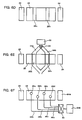
- Figure 6A is a schematic view of a measurement system using a planar waveguide with a species-specific clad segment.
- Figures 6B-F are various embodiments of measurement systems utilizing planar waveguides with two or more species-specific clad segments.
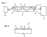
- Figure 7 is a side view of a planar waveguide measurement system including means for blocking light which propagates straight down the waveguides.
- Figure 8 is a side view of a waveguide with a clad segment formed of two layers of different materials.
-
- A waveguide sensor will now be described with at least one clad segment wherein the index of refraction of the waveguide clad segment and waveguide body have been selected relative to the index of the species of interest to produce a controlled leakage of light from the waveguide through the clad segment when the species of interest contacts the clad segment. The transmission properties of the waveguide thus vary as the refractive index of the species of interest present in the surrounding medium (in liquid or vapor or water emulsion form), and thus provide a measure of the refractive index. The clad segments are also chosen for their specificity to particular species of interest so that the sensor response identifies the species.
- The waveguide body and clad segment materials are selected with indexes N1, N3 to optimize the effect of the refractive index of the chemical species of interest. Both selective affinity and refractive index must be considered to get required specificity and sensitivity. In a mixture it is the average refractive index which is measured, i.e. the refractive index is one number which is determined by all the species present and their concentrations. Sorting, or enhancing the response of a particular species or group of compounds, is thus a prerequisite to a refractive index measurement.
- The proper matching of the refractive indexes N1, N2, N3, N4 in configuring the waveguide sensor produces an optimized sensor tailored to a particular species. The species of interest has a refractive index N4. The clad segment is formed of a material with index N3 which has a known affinity for the particular chemical species. When the species of interest contacts the clad segment on the waveguide, a refractive index N* is produced which is a function of both N3 and N4. The choice of the clad segment material, as well as various characteristics of the clad segment such as thickness and porosity, in combination with the chemical species of interest thus produce the refractive index N* seen by the waveguide sensor in the interaction region. For the waveguide to leak light, the index N* must be greater than N1 so a suitable material for the waveguide can be selected. Once the waveguide material is selected, the remaining clad material with index N2 can be selected. The index N2 must be less than N1 and is preferably at least about 10% less so that the critical angle is relatively large and a significant amount of the input light signal will be totally internally reflected down the waveguide. The index N2 and the position of the clad segment(s) should also be selected so that a significant portion of the totally internally reflected light beam is incident on the clad segment(s).
- As shown in Figure 1 an
optical waveguide 10 is toned of a planaroptical waveguide body 12 having a refractive index N1 and aclad 14 having a refractive index N2 less than N1 formed thereon. Thewaveguide body 12 forms the light guiding means through which the light is guided, similar to the core of an optical fiber. The optical waveguide operates by total internal reflection of light at thewaveguide body 12/clad 14 interface since the index N2 is less than N1 for all light within an angle determined by the ratio N2/N1. (Only details of the sensingsurface containing clad 14 are shown, although the opposed surface would be mounted on a suitable substrate or be coated with a suitable coating to produce total internal reflection within thewaveguide 12.) Thewaveguide 12 also has a pair ofend surfaces 16 for inputting and outputting a light signal. - As shown in Figure 2, the
clad 14 onwaveguide body 12 contains aclad segment 18 of different refractive index N3. With reference to Figure 2, the chemical species of interest has an index N4. The material ofclad segment 18 is chosen so that it is specific to a species of interest and has an index N3 which in combination with the index N4 of the species of interest when present in the surrounding medium and the index N1 of the waveguide produces a controlled light leakage from which the presence of the species of interest can be determined. - The operation of the waveguides of Figures 1 and 2 to transmit light are illustrated in Figures 3A and 3B, respectively. In Figure 3A the light is input through one
end face 16 ofwaveguide 12 and is totally internally reflected at the interface betweenwaveguide 12 andclad 14 until it is output through theother end face 16. (As previously described, total internal reflection also occurs on the opposed surface ofwaveguide 12 from clad 14 by suitable means.) End faces 16 are preferably at angles as shown to eliminate light reflection on entrance and exit from the waveguide. In Figure 3B, clad 14 continues to produce total internal reflection of the light within thewaveguide 12 but cladsegment 18 allows a controlled amount of the light to leak from the waveguide, thereby reducing the light output signal from the waveguide. Light leakage is controlled by the selection of the index N1 of the waveguide and index N3 of the clad segment so that in combination with the index N4 of the species of interest, the effect is optimized. - As illustrated in Figure 3C, the light transmissivity or leakage is controlled by the clad
segment 18 which is shown as having pores (cells) 19 into which atoms ormolecules 17 of the species of interest are absorbed. The combination of the clad 18 and absorbedspecies 17 produces a localized refractive index which is used to control light leakage. - As illustrated in Figure 4, the clad
segments 18a, b,c,d,e can take a variety of shapes and orientations including stripes in any direction on the surface or square or circular areas. The ease of producing patterned coatings on a planar waveguide surface, using conventional technology such as photoresist, masking, and etching from the semiconductor field, provides great flexibility in making clad segments which maximize contact with the sample. - The light intensity of the signal transmitted through the waveguide, thus will vary as a function of the presence of the chemical species of interest which causes a light loss during the transmission. The result of changes in the output signal are illustrated in Figure 5. The dynamic range of the sensor is designed to provide easy measurement of the species in the concentration range of interest, i.e. the sensor is designed to produce a large signal change for a selected range of species concentration. By appropriate choice of the sensor parameters, the light loss that occurs over a measurement range of interest is a significant percentage of the total light signal (no loss) so that the signal difference can be easily measured. Choice of light intensity and wavelength also can be used to obtain the desired dynamic range.
- A simple sensor system 29 utilizing the waveguide sensor is illustrated in Figure 6A. The
waveguide 26 having a cladsegment 28 formed thereon is placed between asource 22 anddetector 24.Suitable optics detector 24 is input into processing means 27 such as a digital computer to record, display, and otherwise process the signals. Althoughclad segment 28 is shown as a stripe oriented along the axis between the source and detector, other orientations or shapes of the clad segment could be used. When the surrounding medium which contacts the cladsegment 28 on the surface ofwaveguide 26 contains a species of interest for which thewaveguide 26/cladsegment 28 have been designed, light leakage occurs so that the detected light intensity of the signal propagated through the waveguide decreases. Light sources including lasers (e.g., diode lasers), lamps, or LEDs can be used. The detector may be a photodiode. - Various embodiments of the dual/multiple measurement approach are shown in Figures 6B-F. As shown in Figure 6B,
waveguide 26 is formed with a pair of spaced parallelclad segments 28a,b each of which has a different specificity to a particular chemical species or group of chemical species. A pair ofsources 22a,b and a pair ofdetectors 24a,b are positioned around thewaveguide 26, with one of each pair aligned with one of the cladsegments 28a,b. By using highlydirectional sources 22a,b, or by using additional optics, the light beam fromsource 22a todetector 24a will be affected byclad segment 28a but not significantly byclad segment 28b, and light fromsource 22b todetector 24b will be affected only byclad segment 28b; i.e., the light beams from the two sources will propagate along separate channels or portions of the waveguide and each will only be affected by one clad segment. The outputs ofdetectors 24a,b can then be processed to provide desired information. - Alternative configurations include the use of a single source with a pair of detectors or a single detector with a pair of sources. The particular configuration will depend partly on the spectral characteristics of available sources and detectors. Using such arrangements, the effects of each of the clad
segments 28a,b can be measured and the signals processed, e.g. by processing means 27 (Figure 6A) such as a digital computer, to provide desired information about particular chemical species. Of course, the principles can be generalized to more than two clad segments. - As shown in Figure 6C, a
waveguide 26 with spaced parallelclad segments 28a,b is positioned between asingle source 22 anddetector 24. A mechanical shutter orchopper 30 is positioned between thewaveguide 26 anddetector 24 in order to alternately pass the signal produced by one clad segment while blocking the effect produced by the other clad segment. In the configurations of 6B and C, the clad segments should be oriented parallel to the axis between the source and detector to define somewhat separate channels wherein different effects on signal transmission can be detected, either simultaneously (Figure 6B) or alternately (Figure 6C). - However, if suitable sources and detectors are available, a more general configuration of
waveguide 26 withclad segments 28a,b can be positioned between asingle source 22 andsingle detector 24 as shown in Figure 6D. For example, dichromatic LED lamps and color sensors are available. The specificity and sensitivity of a clad segment to a chemical species can also be a function of the wavelength of the light. Thus, a light signal of two wavelengths, each of which is affected differently by the two clad segments can be input and the variation at the two frequencies can be detected. Alternatively, two sources of different wavelengths and/or two detectors can be used. - When the available sources and/or detectors do not allow simultaneous measurement of the effects produced by two different clad segments, it may be possible to perform sequential measurements of these effects. For example, as shown in Figure 6E, the
waveguide 26 withclad segments 28a,b is positioned between asource 22 anddetector 24. Sample fromreservoir 32 is flowed through acontrol valve 36 into a pair of flow channels 34a,b which contact cladsegments 28a,b, respectively. The sample can first be flowed through channel 34a to produce a response due to cladsegment 28a and then flowed throughchannel 34b to produce a response due to cladsegment 28b. - In addition to measuring the light transmitted through the waveguide, it is also possible to measure the light lost through the clad segment. For example, in Figure 6F a waveguide has a plurality of circular clad
segments 28a,b,c,d and is positioned between asource 22 anddetector 24a. Fiber optic or othersuitable detectors 38a,b,c,d are positioned to measure the light leakage through cladsegments 28a,b,c,d, respectively. The signals fromlight sensors 38a,b,c,d pass through amultiplexer 40 into asecond detector 24b so that the light leakage signals can be measured. - The ability to accurately measure the intensity changes caused by leakage through the clad segment is important. As shown in Figure 7, a
waveguide structure 12/14 with cladsegment 18 is positioned between asource 22 anddetector 24. Light from thesource 22 which enterswaveguide body 12 throughend face 16 and is incident on clad 14 at an angle less than the critical angle defined by the refractive index ratio will be totally internally reflected as illustrated. However, some light will propagate substantially down the center of the waveguide; this is particularly so whensource 22 is not highly directional. This unreflected light passes straight down the waveguide and provides a large background signal atdetector 24. To reduce or eliminate this problem, detector masking means 42 can be positioned ondetector 24 and/or detector masking means 44 can be positioned onend face 16 to substantially block the unreflected background light which passes straight down the center of the waveguide while permitting substantially all the totally internally reflected light to reach the detector. - The refractive index and sensitivity of the clad segment are important parameters of the waveguide sensor. However, in some circumstances the available materials may not provide the desired values. One approach, as illustrated in Figure 8 is to form clad
segment 18 of two different materials, e.g. athin metal layer 46 overcoated by a polymer layer 48, or vice-versa, which together produce the desired properties. For example,metal layer 46 can be chosen for its affinity to the species and polymer 48 (which is permeable to the species) can provide the desired refractive index N3 of clad segment 18 (N3 will be determined by index N5 oflayer 46 and index N6 of layer 48). The refractive index of select metals, at various wavelengths, are listed in Table 1 and the refractive index of select polymers is shown in Table 6. Combinations of these can be used as described. - A further possibility to provide selectivity of the clad segment where a suitable material is not available, but a good material is available which is specific to a reaction product of the species, is to include a catalyst in the clad segment.
Clad segment 18 can include a catalyst embedded or dispersed therein, or a separate catalyst layer can be applied on the species-specific clad layer, e.g. in Figure 8,layer 46 is the specific clad material and layer 48 is the catalyst. The catalyst will catalyze a reaction of the species of interest to form a reaction product to which the clad segment has strong affinity. As an example, TCE could be detected by a waveguide sensor having a clad segment specific to HCl and a catalyst to react with the TCE to form HCl. - The specificity or affinity of the clad has been further defined in terms of various parameters, particularly surface structure as well as crystallographic orientation. A methodology for tailoring a waveguide sensor to a particular chemical species by appropriate choice of the refractive indexes is provided. Multiple clad segments are used to identify a particular species from a group of species which interact with some clad materials. A clad segment of two different materials, one to provide refractive index and the other to provide species selectivity, can be used, as well as a clad segment with a catalyst to react the species of interest to provide a reaction product for which the clad segment has a strong affinity.
- The substrate is usually glass or quartz. This material has a refractive index of 1.47(6) at 400 nm, 1.46(2) at 500 nm and 1.45(7) at 650 nm. Special substrates can be made of a variety of materials, e.g., NaCl, N=1.54(4); AgCl, N=2.07(1); Ag2SO4, N=1.75(8); MgF2, N=1.378; Li2SO4, N=1.46(5), and Al2(SO4)3, N=1.47. In fact, any material which can be made into a plate which can propagate light is a possible substrate.
- In the waveguide structures according to the invention, the clad segments are typically about a monolayer to about 50 Å thick. The waveguide body must have sufficient rigidity so that the light propagation pattern is not affected by flexing.
- These thin metal clads can be chosen with an effective light porosity or tranmissivity when in contact with a species of interest to change the light transmission through the waveguide as a function of the refractive index of the chemical species of interest present in the surrounding medium. The light porosity of the clad is a function of the clad material, its thickness and its physical characteristics such as physical porosity and crystalline structure. The metal clad is selected of a suitable thickness to produce a gradient refractive index at the interface between the waveguide body and the clad segment as a result of chemical species of interest from the surrounding medium being absorbed on the metal clad. This localized refractive index at the boundary between the waveguide body and clad segment is directly proportional to the amount of the chemical species adsorbed/absorbed on the clad segment and also its refractive index. The amount of light leaking from the waveguide through the clad depends on the amount and refractive index of the chemical species. The light leakage substantially modulates the light signal transmitted through the core, producing a detectable measure of the presence of the chemical species and its refractive index.
- The metal coatings are key to the selection process. They are selected both because they have specific affinity to various species and because they have appropriate refractive indexes. The index of refraction of several metals, for several wavelengths, are given in Table 1.
Wavelength (nm) Photon Energy (ev) Refractive Index (Cr) (Ni) (Rh) (Pt) 990 1.25 4.50 2.91 3.39 3.42 660 1.88 3.66 2.10 2.22 2.48 550 2.26 3.31 1.78 1.98 2.13 480 2.59 2.22 1.65 1.85 1.92 - The affinity depends on the metal selected, the thickness of the coating and the method of attachment. The crystal structure and orientation is very important in the selectivity process. Furthermore, the more ordered the crystal, the better it behaves as a sensing material, e.g., Ni(111) and Ir(110) both absorb benzene, but the Ni(111) is ordered while the Ir(110) is disordered and the Ni(111) performs much better. The type of absorption, i.e., mechanical, chemical, electrostatic, solvation, etc. also determines the effectiveness of the metal coating.
- The metal claddings that may be utilized as the clad segments on the waveguide include:
- 1) group IVB elements: Titanium (Ti), Zirconium (Zr), Hafnium (Hf);
- 2) group VB elements: Vanadium (V), Niobium (Nb), Tantalum (Ta);
- 3) group VIB elements: Chromium (Cr), Molybdenum (Mo), Tungsten (W);
- 4) group IB elements: Copper (Cu), Silver (Ag), Gold (Au);
- 5) group IIB elements: Zinc (Zn), Cadmium (Cd);
- 6) group VIII elements: Iron (Fe), Ruthenium (Ru), Cobalt (Co), Rhodium (Rh), Nickel (Ni), Palladium (Pd), Platinum (Pt), Iridium (Ir), Osmium (Os);
- 7) Oxides of the above metals;
- 8) Metal compounds or alloys such as:
- a) group II-VI compounds: including but not limited to ZnSe, ZnTe, CdS, CdTe, MgTe, ZnS;
- b) group III-V compounds: including but not limited to BN, GaAs, InAs, InSb, AlN, GaN, InN;
- c) group I-VII compounds: including but not limited to CuCl, CuBr, AgI;
- d) sphalerite structure compounds: including but not limited to Ga2Te3, ZnSnP2, ZnSnAs2;
- e) Wurtzite structure compounds: including but not limited to SiC, MnS, MnSe, MnTe, Al2Se3;
- f) group I, III, VI compounds: including but not limited to CuGaTe2, CuGaSe2, CuLaS2;
- g) group II, IV, V compounds: including but not limited to ZnGeP2, CdGeP2, ZnGeAs2, ZnSnAs2.
-
- The metal coatings can be deposited on the waveguide surface by sputtering, brush coating, vacuum deposition, plasma coating, or by any other technique that can form either a homogeneously- or heterogeneously-coated surface. Various lithographic techniques can be used to produce the appropriate clad segment patterns. Either inorganic or organometallic compounds can be used to deposit metal coatings on the waveguide. The metals can also be deposited from their elemental states. The final coating deposited on the waveguide can be in the form of either elemental metal or any of its oxides or other metal compounds or alloys.
- The clad segments are made of materials which have a strong affinity for the chemical species of interest. The affinity is determined by a number of different factors such as chemical or mechanical adsorption, pore size, electrostatic attraction, or ability to dissolve the species. The affinity of the clad segment for the species is illustrated in Figure 3C in which atoms or
molecules 17 of the species are adsorbed in pores 19 (indicated by cell structure) formed inclad segment 18. - The metal clads show varying sensitivities or selectivities for different chemical species. The variation of sensor response to various chemical species is illustrated in Table 2 where V0 is the detector voltage output in the absence of the chemical species (i.e., no light leakage) and V is the detector output voltage in the presence of a given amount of the chemical species. Certain metals are particularly sensitive to certain chemical species while relatively insensitive to others. Each chemical species can be detected by a number of different metal dads.
Ru V0 V Gasoline 7.27 3.87 Benzene 7.00 4.19 Xylene 7.38 4.39 Toluene 7.07 4.10 V Gasoline 6.85 5.80 Benzene 5.32 3.79 Zr Gasoline 8.20 5.89 Benzene 8.00 2.28 Xylene 7.68 3.62 Toluene 7.51 4.57 Ni Gasoline 9.46 6.74 Benzene 7.48 1.07 Xylene 8.56 1.27 Toluene 8.16 1.77 Pd Gasoline 7.51 4.92 Benzene 8.00 6.78 Xylene 7.44 5.00 Fe Benzene 8.96 1.65 - Table 3 lists a number of illustrative metal surfaces and various gases which have been found to be adsorbed on the metal surface. The adsorbability of the gases may depend on the crystal form and/or orientation of the metal layer. In the process of forming the metal clad segment on the waveguide, particular crystal forms of the metal can be reproducibly obtained by controlling the process parameters, e.g. temperature and pressure, so that a sensor tailored to a specific gas can be obtained. Thus, a sensor with a metal clad segment of preselected crystal structure can be produced for use with a desired analyte. Table 4 similarly lists a number of illustrative metal surfaces and various organic compounds (hydrocarbons) which have been found to be adsorbed on the metal surface. Certain metals, and in some cases certain crystal forms of some metals, are thus particularly suitable for the metal clad segment for detection of certain hydrocarbons. The lists of Tables 3 and 4 are only for purposes of illustration and are not exhaustive of all possible combinations. Further information about adsorption of gases by metal surfaces is contained in Chemistry In Two-Dimensional Surfaces, Garbor A. Somorjai, Cornell Univ. Press, Ithaca, NY, 1981, particularly Tables 5.2-5.7, pp. 210-241, which are herein incorporated by reference.
SURFACE ADSORBED GAS A1 (111), (100), (110) O2 Au (111) O2 (100) H2S, CO, Xe Cu (111) O2, CO, Cl2, H2S, Xe (100) O2, CO, N2 (110) O2, CO, H2O, H2S, Xe Cu/Ni (111) CO (110) O2, CO, H2S Fe (111) O2, NH3, H2 (100) O2, CO, H2S, H2, NH3, H2O (110) O2, CO, N2, H2, H2S Fe/Cr (100), (110) O2 Mo (111) O2, H2S (100) O2, CO, H2, N2, H2S (110) O2, CO, CO2, H2, N2, H2S Ni (111) O2, CO, CO2, H2, NO, H2S, H2Se, Cl2 (100) O2, CO, CO2, H2, H2S, Te, Xe (110) O2, CO, H2, NO, H2O, H2S, H2Se NiO (101) H2, H2S, Cl2 Pt (111) O2, CO, H2, NO, H2O, S2, N (100) O2, CO, H2, NO, N, H2s, S2 (110) O2, CO, C3O2, NO, H2S Rh (111), (100) O2, CO, CO2, H2, NO (110) O2, CO Zn ZnO (0001) O2 (1010) O2 SURFACE ADSORBED GAS Fe (100) C2H4 Ir (111) C2H2, C2H4, cyclohexane, benzene (100) C2H2, C2H4, benzene (110) C2H4, benzene Mo (100) CH4 Ni (111) CH4, C2H2, C2H4, C2H6, cyclohexane, benzene (100) CH4, C2H2, C2H4, C2H6, benzene (110) CH4, C2H4, C2H6, C5H12 Pt (111) C2H2, C2H4, n-butane, n-petane, n-hexane, n-heptane, n-octane, cyclohexane, benzene, toluene, naphthalene, pyridine, m-xylene, mesitylene, T-butylbenzene, N-butylbenzene, aniline, nitrobenzene, cyanobenzene (100) C2H2, C2H4, benzene, naphthalene, pyridine, toluene, M-xylene, mesitylene, T-butylbenzene, N-butylbenzene, aniline, nitrobenzene, cyanobenzene, C2N2 (110) HCN, C2N2 Rh (111),(100),(331) C2H2, C2H4 - The specificity of different metal clads to various analytes allows more specific analysis of an analyte mixed with other substances. The invention further includes multiple measurement methods and apparatus. Since more than one clad may be available for a particular analyte, but each clad will not have the same absorption coefficients to other analytes, a more complex measurement method and sensor structure can be used to determine the presence of a selected analyte out of a mixture of several different analytes. To detect analyte A in a mixture of analytes A and B, it would be most desirable to find a single metal surface that is specific to A. However, if one cannot be found, two sensors can be used, one which has a clad which responds to both A and B and one which has a clad which responds to B but not A. By subtracting the measurement obtained from the second sensor from that of the first sensor, a measure of analyte A is obtained.
- Alternatively, if a specific metal clad is not available for either A or B, then clads are chosen which have different absorption coefficients for A and B, and the concentration of A and B are obtained by solving an algorithm for two unknowns. The dual sensor approach can be extended to multiple sensors for more than two analytes and can be implemented in a variety of ways, using either a single waveguide or multiple waveguides.
- The crystallographic orientation of the metal coatings is particularly important since the affinity of various chemical species is often strongly dependent on the crystallographic form of the metal. The planar waveguide is a highly advantageous structure for depositing clad segments having preferred crystallographic orientations, since deposition on a flat surface is much easier to perform using known deposition techniques.
- In accordance with the invention, and as shown in Table 5, pairs of clad segments, each responsive to different combinations of different chemical species, can be used to detect a particular species by subtracting one response from another when a particular clad which responds directly to a single species is not available.
Be (0001) O2, CO, H2, N2 Cu (100) O2, CO, N2 [Be(0001)] - [Cu (100)] H 2 Mo (100) O2, CO, H2, N2, H2S Be (0001) O2, CO, H2, N2 [Mo (100)] - [Be (0001)] H 2 S Co (100) CO, O2 Cr (100) O 2 [Co (100)] - [Cr (100)] CO Mo (110) O 2 , CO, CO2, H2, N2, H2S Mo (100) O2, CO, H2, N2, H2S [Mo (110)] -[Mo (100)] CO 2 Ru (101) O2, CO, NO Co (100) O2, CO [Ru (101)] - [Co (100)] NO - In addition to the crystallographic orientation of the surface, the surface structure itself provides specificity. For example, Pt(111) adsorbs n-butane, n-pentane, n-hexane, and n-octane. If the surface structures are considered, preference can be attained. The preferred structures of the Pt(111) surface for these species are:
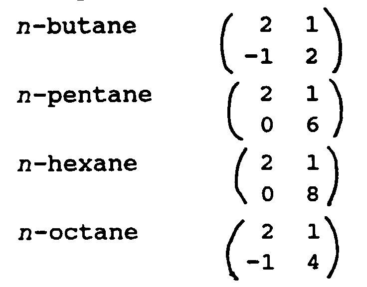
- For these linear molecules, therefore,is the general surface structure. It is important to note that for cyclohexane, this changes and the surface structure becomes

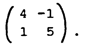
- Therefore, according to the invention, by forming clad segments of particular materials, with particular crystallographic orientations and specific surface structures, specificity for individual species can be better achieved.
- The Pt(111) example illustrates the use of different surface structures of a material to select between closely related compounds with very similar chemical structures. The ability to distinguish between compounds with very similar chemical structures, without doing a detailed spectral analysis, is very important to sensor technology. The same approach is applicable to separate benzene, toluene, and xylene.
- Whereas the surface structures give good species separation, improvements can be made on specificity by further focusing on refractive index differences. This can be accomplished in two (2) ways: (i) undercoating or overcoating the metal film; and (ii) adjusting the refractive index of the substrate (N1) by selecting a suitable material for the substrate.
- The overcoating (or undercoating) of the metal film will, among other materials, be a polymer. These materials, nominally, have refractive indexes between 1.34 and 1.64. Examples of these are given in Table 6.
Compound Refractive Index Poly(tetrafluoroethylene-co-hexafluoropropylene) 1.338 Poly(pentafluoropropyl acrylate) 1.385 Poly(butyl acrylate) 1.466 Poly(n-butyl methacrylate) 1.481 Cellulose Nitrate 1.500 Poly (N-benzyl methacrylamide) 1.596 - It is possible to find metal surfaces which will selectively adsorb target compounds. This can range from a single species to a group of compounds. These surfaces are anything but perfect when it comes to completely isolating a particular target and secondary species sorting may help. As an example, in environmental analysis, separation and analysis of the organic chlorides is an important task. Typical compounds are chloroform [N = 1.448(6)], trichloroethylene (TCE) [N = 1.477(5)], and the chlorophenols [N2-chloro = 1.557(9), N3-chloro = 1.556(5), N4-chloro = 1.541(9)]. The metal is chosen to selectively adsorb the organic chlorides while an overcoating (or undercoating) is used to control light leakage. For the above compounds, if the overcoating has 1.448 < N < 1.477 (e.g., cellulose acetate butyrate) only the chloroform controls the light. As shown in Table 7, proper selection of overcoating makes species concentrations available by difference.
Species Compound Nc Typical Overcoat No Measured Species 1 Chloroform 1.448 cellulose acetate butyrate 1.460 1 2 TCE 1.477 Poly(n-butyl methacrylate) 1.480 1+2 3 4-chlorophenol 1.541 Poly(N-allyl methacrylate) 1.547 1+2+3 4 3-chlorophenol 1.556 Epoxy Resin 1.557 1+2+3+4 5 2-chlorophenol 1.557 Poly(benzyl methacrylate) 1.568 1+2+3+4+5 - For example, to obtain inputs on 3-chlorophenol (species 4) subtract 3 from 4, i.e., [(1+2+3+4) - (1+2+3) = 4].
- Changes and modifications in the specifically described embodiments can be carried out without departing from the scope of the invention which is intended to be limited only by the scope of the appended claims.
Claims (16)
- A waveguide sensor (10) for measuring refractive index and identifying chemical species of a surrounding medium, comprising:an optical waveguide body (12) having a refractive index N1;a clad (14) including a thin film metal clad segment (18) of metal or metal oxide or other metal compound or alloy formed on the surface of the waveguide body (12), the metal clad segment (18) having a refractive index N3, and an effective thickness and light transmissivity which in combination with the surrounding medium produces a localized refractive index N* such as to cause a controlled leakage of light from the waveguide body (12) which modulates the transmission of light through the optical waveguide body (12) as a function of the refractive index of the surrounding medium, the remainder of the clad (14) having a refractive index N2 less than N1;a light source (22) operatively associated with the optical waveguide body (12) for inputting a light signal into the optical waveguide body (12);detection means (24) operatively associated with the optical waveguide body to detect signals produced by said modulation; andprocessing means for calculating information about a particular compound of interest from the signals produced by said modulation;
characterised in that the optical waveguide body (12) is planar, having a flat surface bearing the clad as a patterned coating thereon; the clad having a plurality of metal clad segments (28a, 28b...), each having different selectivity to chemical species of interest, including a pair of metal clad segments (18, 28a...) selected from:in that the detection means comprises means for detecting a signal produced by each of the pair of metal clad segments and the processing means comprises means for subtracting the signals produced by the pair of metal clad segments from one another.a) Be (0001) and Cu (100);b) Mo (100) and Be (0001);c) Co (100) and Cr (100);d) Mo (110) and Mo (100);e) Ru (101) and Co (100); and - The sensor of Claim 1 further comprising an overlayer or underlayer (46, 48) of a second material on the metal clad segment, the metal clad segment having a strong affinity for a chemical species of interest, the second material having a suitable refractive index to produce controlled light leakage in the presence of the chemical species.
- The sensor of Claim 2 wherein the second material is a polymer with a refractive index in the range or about 1.34 to about 1.64.
- The sensor of Claim 3 wherein the polymer is selected from poly(tetrafluoroethylene-cohexafluoropropylene), poly(pentafluoropropyl acrylate), poly(butyl acrylate), poly(n-butyl methacrylate), cellulose nitrate, and poly(N-benzyl methacrylamide).
- The sensor of Claims 1 to 4 further comprising a catalyst on the metal clad segment for reacting with the species of interest to form a reaction product, wherein the metal clad segment is specific to the reaction product.
- The sensor of Claims 1 to 5 wherein the optical waveguide body (12) is formed of SiO2 (glass/quartz), NaCl, AgCl, Ag2SO4, MgF2, Li2SO4, or Al2(SO4)3.
- A method of detecting the refractive index and identifying chemical species of a medium, comprising:providing a waveguide sensor (10) according to claim 1;contacting the thin film metal clad segments (18) with the medium;inputting a light signal from said source (22) into the optical waveguide body (12);detecting the signals produced by each of the pair of metal clad segments;and subtracting the signals from one other.
- The method of Claim 7 further comprising forming an overlayer or underlayer (46, 48) of a second material on the metal clad segment, the metal clad segment having a strong affinity for a chemical species of interest, the second material having a suitable refractive index to produce controlled light leakage in the presence of the chemical species.
- The method of Claim 7 or 8 further comprising adding a catalyst to the metal clad segment for reacting the species of interest to form a reaction product and forming the metal clad segment specific to the reaction product.
- A method of forming a refractive index waveguide sensor comprising:providing an optical waveguide body (12) having a refractive index N1; forming a clad on the optical waveguide body;the clad (14) including a thin film metal clad segment (18) of metal or metal oxide or other metal compound or alloy formed on the surface of the waveguide body (12), the metal clad segment (18) having a refractive index N3, and an effective thickness and light transmissivity which in combination with the surrounding medium produces a localized refractive index N* such as to cause a controlled leakage of light from the waveguide body (12) which modulates the transmission of light through the optical waveguide body (12) as a function of the refractive index of the surrounding medium, the remainder of the clad (14) having a refractive index N2 less than N1;providing a light source (22) operatively associated with the optical waveguide body (12) for inputting a light signal into the optical waveguide body (12);providing detection means (24) operatively associated with the optical waveguide body to detect signals produced by said modulation; andproviding processing means for calculating information about a particular compound of interest from the signals produced by said modulation;
characterised in that the optical waveguide body (12) is planar, having a flat surface bearing the clad as a patterned coating thereon; the clad having a plurality of metal clad segments (28a, 28b...), each having different selectivity to chemical species or interest, including a pair of metal clad segments (18, 28a...) selected from:in that the detection means comprises means for detecting a signal produced by each of the pair or metal clad segments and the processing means comprises means for subtracting the signals produced by the pair of metal clad segments from one another.a) Be (0001) and Cu (100);b) Mo (100) and Be (0001);c) Co (100) and Cr (100);d) Mo (110) and Mo (100);e) Ru (101) and Co (100); and - The method of Claim wherein the step of forming the metal clad segment (18) on the portion of the optical waveguide body is performed by sputtering, vacuum deposition, plasma coating, brush coating, or spin coating of said metal.
- The method of Claim 10 or 11 further comprising applying an over/underlayer (46, 48) of a second material on the metal clad segment (18), the metal clad segment (18) having a strong affinity for a chemical species of interest, the second material having a suitable refractive index to produce controlled light leakage in the presence of the chemical species.
- The method of Claims 10 to 12 further comprising applying a catalyst on the metal clad segment (18) for reacting with a species of interest to form a reaction product, wherein the metal clad segment (18) is specific to the reaction product.
- The sensor according to claim 1 comprising alternative viewing means positioned between the optical waveguide body and detection means for alternatively passing a light beam affected by one of the clad segments while blocking a light beam affected by the other clad segment.
- The sensor according to claim 1 further comprising means for alternatingly flowing a sample over one of the metal clad segments while preventing flow over the other metal clad segments.
- The sensor according to claim 1 further comprising light blocking means positioned on at least one of the optical waveguide body detection means for substantially blocking background light passing straight down the center of the optical waveguide body from reaching the detection means.
Applications Claiming Priority (3)
| Application Number | Priority Date | Filing Date | Title |
|---|---|---|---|
| US07/646,148 US5165005A (en) | 1988-01-29 | 1991-01-24 | Planar and other waveguide refractive index sensors using metal cladding |
| US646148 | 1991-01-24 | ||
| PCT/US1992/000612 WO1992014177A2 (en) | 1991-01-24 | 1992-01-24 | Planar and other waveguide refractive index sensors using metal cladding |
Publications (3)
| Publication Number | Publication Date |
|---|---|
| EP0568652A1 EP0568652A1 (en) | 1993-11-10 |
| EP0568652A4 EP0568652A4 (en) | 1994-05-18 |
| EP0568652B1 true EP0568652B1 (en) | 2000-10-11 |
Family
ID=24591961
Family Applications (1)
| Application Number | Title | Priority Date | Filing Date |
|---|---|---|---|
| EP92908461A Expired - Lifetime EP0568652B1 (en) | 1991-01-24 | 1992-01-24 | Waveguide sensor |
Country Status (8)
| Country | Link |
|---|---|
| US (1) | US5165005A (en) |
| EP (1) | EP0568652B1 (en) |
| JP (1) | JPH06505556A (en) |
| AT (1) | ATE196951T1 (en) |
| AU (1) | AU1642592A (en) |
| CA (1) | CA2101072A1 (en) |
| DE (1) | DE69231502T2 (en) |
| WO (1) | WO1992014177A2 (en) |
Families Citing this family (49)
| Publication number | Priority date | Publication date | Assignee | Title |
|---|---|---|---|---|
| US5777726A (en) * | 1992-05-12 | 1998-07-07 | Raytheon Company | Spectrophotometric supercritical fluid contamination monitor |
| US5253037A (en) * | 1992-08-04 | 1993-10-12 | Fci-Fiberchem, Inc. | Optimal length for refractive index sensors |
| US5323477A (en) * | 1992-08-24 | 1994-06-21 | Motorola, Inc. | Contact array imager with integral waveguide and electronics |
| EP0598341B1 (en) * | 1992-11-17 | 1998-09-23 | Hoechst Aktiengesellschaft | Optical sensor for detecting chemical species |
| CA2117003A1 (en) * | 1993-04-13 | 1994-10-14 | Dana Craig Bookbinder | Method of encapsulating optical components and products produced by that method |
| WO1994024543A1 (en) * | 1993-04-15 | 1994-10-27 | Japan Energy Corporation | Total reflection type sensor for measuring refraction index |
| US5439647A (en) * | 1994-02-25 | 1995-08-08 | Fiberchem, Inc. | Chip level waveguide sensor |
| US5737457A (en) * | 1994-02-25 | 1998-04-07 | Fci - Fiberchem, Inc. | Chip level waveguide sensor |
| US5615008A (en) * | 1994-12-21 | 1997-03-25 | Beckman Instruments, Inc. | Optical waveguide integrated spectrometer |
| TW302435B (en) * | 1995-05-12 | 1997-04-11 | Ciba Geigy Ag | |
| US5619599A (en) * | 1995-05-12 | 1997-04-08 | Xerox Corporation | Remote split scan detector |
| US5719033A (en) * | 1995-06-28 | 1998-02-17 | Motorola, Inc. | Thin film transistor bio/chemical sensor |
| US5822473A (en) * | 1996-02-29 | 1998-10-13 | Texas Instruments Incorporated | Integrated microchip chemical sensor |
| US6149591A (en) * | 1997-02-21 | 2000-11-21 | Duke University | Refractometric devices especially adapted for the in vivo detection of refractive indices of cervical mucus |
| US6432364B1 (en) * | 1998-07-06 | 2002-08-13 | Suzuki Motor Corporation | SPR sensor cell and immunoassay apparatus using the same |
| EP0971226A1 (en) * | 1998-07-06 | 2000-01-12 | Suzuki Motor Corporation | SPR sensor cell and immunoassay apparatus using the same |
| US6035705A (en) * | 1998-09-01 | 2000-03-14 | Marathon Ashland Petroleum Llc | Method for characterization of fuels |
| US6821738B2 (en) * | 1999-01-20 | 2004-11-23 | The Board Of Regents For Oklahoma State University | Broad spectrum bio-detection of nerve agents, organophosphates, and other chemical warfare agents |
| US6381025B1 (en) | 1999-08-19 | 2002-04-30 | Texas Tech University | Interferometric detection system and method |
| US6694067B1 (en) | 2001-01-05 | 2004-02-17 | Los Gatos Research | Cavity enhanced fiber optic and waveguide chemical sensor |
| US6809828B2 (en) | 2001-01-25 | 2004-10-26 | Texas Tech University | Universal detector for biological and chemical separations or assays using plastic microfluidic devices |
| GB2375188B (en) * | 2001-04-30 | 2004-07-21 | Samsung Electronics Co Ltd | Wearable Display Apparatus with Waveguide Having Diagonally Cut End Face |
| US6707958B2 (en) * | 2001-11-20 | 2004-03-16 | Agilent Technologies, Inc. | Biochemical assay device using frustrated total internal reflection modulator with an imaging optical waveguide |
| RU2219525C2 (en) * | 2002-01-29 | 2003-12-20 | Общество с ограниченной ответственностью "ВИНТЕЛ" | Method of analysis of chemical composition of substances in liquid and gaseous environment with extractive concentration and facility for its realization |
| US7435391B2 (en) * | 2003-05-23 | 2008-10-14 | Lucent Technologies Inc. | Light-mediated micro-chemical reactors |
| US8599140B2 (en) * | 2004-11-17 | 2013-12-03 | International Business Machines Corporation | Providing a frustrated total internal reflection touch interface |
| US7391936B2 (en) * | 2005-01-21 | 2008-06-24 | Lucent Technologies, Inc. | Microfluidic sensors and methods for making the same |
| US20070053179A1 (en) * | 2005-09-08 | 2007-03-08 | Pang Slew I | Low profile light source utilizing a flexible circuit carrier |
| KR100754686B1 (en) * | 2006-03-28 | 2007-09-03 | 삼성전자주식회사 | Keypad assembly |
| KR100860763B1 (en) | 2006-10-19 | 2008-09-29 | 부산대학교 산학협력단 | Plastic thin film optical waveguide, its manufacturing method and anti-jamming sensor using the optical waveguide |
| KR100827175B1 (en) * | 2007-02-23 | 2008-05-02 | 삼성전자주식회사 | Waveguide Sheet and Manufacturing Method Thereof |
| US8445217B2 (en) | 2007-09-20 | 2013-05-21 | Vanderbilt University | Free solution measurement of molecular interactions by backscattering interferometry |
| US20100236625A1 (en) * | 2009-02-20 | 2010-09-23 | John Kenney | Solar Modules Including Spectral Concentrators and Related Manufacturing Methods |
| US8774573B2 (en) * | 2009-02-20 | 2014-07-08 | OmniPV, Inc. | Optical devices including resonant cavity structures |
| US20100224248A1 (en) * | 2009-02-20 | 2010-09-09 | John Kenney | Solar Modules Including Spectral Concentrators and Related Manufacturing Methods |
| US9638632B2 (en) | 2010-06-11 | 2017-05-02 | Vanderbilt University | Multiplexed interferometric detection system and method |
| US9562853B2 (en) | 2011-02-22 | 2017-02-07 | Vanderbilt University | Nonaqueous backscattering interferometric methods |
| US9262011B2 (en) * | 2011-03-30 | 2016-02-16 | Smart Technologies Ulc | Interactive input system and method |
| DE102011089703B3 (en) * | 2011-12-22 | 2013-05-23 | Continental Automotive Gmbh | Optical measuring arrangement for determination of e.g. light speed within diesel fuel in motor car, has light sources whose light is incident at certain angle different from another angle and reflected to light sensors |
| US9273949B2 (en) | 2012-05-11 | 2016-03-01 | Vanderbilt University | Backscattering interferometric methods |
| US20150233885A1 (en) * | 2014-02-14 | 2015-08-20 | Chevron U.S.A. Inc. | Sorption-based sensing system |
| US9377353B2 (en) * | 2014-06-27 | 2016-06-28 | Intel Corporation | Optical perspiration sensor using frustrated total internal reflection |
| US9680271B2 (en) * | 2014-09-22 | 2017-06-13 | Mcgill University | Sensor systems and methods for analyte detection |
| WO2016118812A1 (en) | 2015-01-23 | 2016-07-28 | Vanderbilt University | A robust interferometer and methods of using same |
| US10627396B2 (en) | 2016-01-29 | 2020-04-21 | Vanderbilt University | Free-solution response function interferometry |
| US10197499B2 (en) * | 2016-04-07 | 2019-02-05 | Corning Incorporated | Waveguide sensor with nanoporous surface layer |
| US11344883B2 (en) * | 2018-08-28 | 2022-05-31 | Max-Ir Labs Incorporated | Microfluidic device with integrated waveguides for analyte identification and method of operation thereof |
| CN111948175B (en) * | 2020-08-05 | 2024-07-19 | 浙江大学 | A high-Q and high-FoM metal-medium assisted GMR refractive index sensing chip |
| US11333601B1 (en) * | 2021-04-14 | 2022-05-17 | United States Of America As Represented By The Secretary Of The Air Force | Thermo-optic refractometry |
Family Cites Families (4)
| Publication number | Priority date | Publication date | Assignee | Title |
|---|---|---|---|---|
| DE3680999D1 (en) * | 1985-05-29 | 1991-09-26 | Artificial Sensing Instr Asi A | OPTICAL SENSOR FOR SELECTIVE DETECTION OF SUBSTANCES AND DETECTION OF REFRIGERATION CHANGES IN MEASURING SUBSTANCES. |
| GB2185308B (en) * | 1986-01-10 | 1989-10-25 | Stc Plc | Optical sensor device |
| US5026139A (en) * | 1988-01-29 | 1991-06-25 | Fiberchem Inc. | Fiber optic refractive index sensor using metal cladding |
| US4929049A (en) * | 1988-01-29 | 1990-05-29 | Fiberchem, Inc. | Fiber optic refractive index sensor using a metal clad |
-
1991
- 1991-01-24 US US07/646,148 patent/US5165005A/en not_active Expired - Fee Related
-
1992
- 1992-01-24 EP EP92908461A patent/EP0568652B1/en not_active Expired - Lifetime
- 1992-01-24 CA CA002101072A patent/CA2101072A1/en not_active Abandoned
- 1992-01-24 JP JP4508117A patent/JPH06505556A/en active Pending
- 1992-01-24 AT AT92908461T patent/ATE196951T1/en not_active IP Right Cessation
- 1992-01-24 WO PCT/US1992/000612 patent/WO1992014177A2/en not_active Ceased
- 1992-01-24 DE DE69231502T patent/DE69231502T2/en not_active Expired - Fee Related
- 1992-01-24 AU AU16425/92A patent/AU1642592A/en not_active Abandoned
Also Published As
| Publication number | Publication date |
|---|---|
| EP0568652A4 (en) | 1994-05-18 |
| AU1642592A (en) | 1992-09-07 |
| JPH06505556A (en) | 1994-06-23 |
| US5165005A (en) | 1992-11-17 |
| WO1992014177A3 (en) | 1992-10-15 |
| EP0568652A1 (en) | 1993-11-10 |
| CA2101072A1 (en) | 1992-07-25 |
| DE69231502D1 (en) | 2000-11-16 |
| WO1992014177A2 (en) | 1992-08-20 |
| ATE196951T1 (en) | 2000-10-15 |
| DE69231502T2 (en) | 2001-06-13 |
Similar Documents
| Publication | Publication Date | Title |
|---|---|---|
| US5165005A (en) | Planar and other waveguide refractive index sensors using metal cladding | |
| EP1774290B1 (en) | Multiwavelength optical sensors | |
| US5455178A (en) | Microoptical sensor and method | |
| USRE37473E1 (en) | Diffraction anomaly sensor having grating coated with protective dielectric layer | |
| US5663790A (en) | Method and apparatus for determination of refractive index | |
| US5606633A (en) | Chemical detector employing surface plasmon resonance excited using an optical waveguide configured as an asymmetric waveguide coupler | |
| US5071248A (en) | Optical sensor for selective detection of substances and/or for the detection of refractive index changes in gaseous, liquid, solid and porous samples | |
| US5327225A (en) | Surface plasmon resonance sensor | |
| US6320991B1 (en) | Optical sensor having dielectric film stack | |
| EP0570445B1 (en) | Analytical device | |
| US5026139A (en) | Fiber optic refractive index sensor using metal cladding | |
| US7212692B2 (en) | Multiple array surface plasmon resonance biosensor | |
| US20120218550A1 (en) | Nanohole array biosensor | |
| AU2005263894A1 (en) | Optical sensors | |
| US7505641B1 (en) | Optical biosensor incorporating wavelength encoding of multiple unlabeled analytes | |
| Homola | Surface plasmon resonance biosensors for food safety | |
| Xhoxhi et al. | Interferometric evanescent wave biosensor principles and parameters | |
| Zaz et al. | Plasmon induced transparency and waveguide mode based optical biosensor for self-referencing sensing | |
| US20070014017A1 (en) | Method for generating electromagnetic field distributions | |
| Buchanan-Vega | Applications of the Guided-Mode Resonance Sensor in Multiparametric, Transmissive, and Picomolar Regimes | |
| Wilkinson | Integrated optical chemical and biochemical sensors |
Legal Events
| Date | Code | Title | Description |
|---|---|---|---|
| PUAI | Public reference made under article 153(3) epc to a published international application that has entered the european phase |
Free format text: ORIGINAL CODE: 0009012 |
|
| 17P | Request for examination filed |
Effective date: 19930819 |
|
| AK | Designated contracting states |
Kind code of ref document: A1 Designated state(s): AT BE CH DE DK ES FR GB GR IT LI LU MC NL SE |
|
| RHK1 | Main classification (correction) |
Ipc: G02B 6/02 |
|
| A4 | Supplementary search report drawn up and despatched |
Effective date: 19940329 |
|
| AK | Designated contracting states |
Kind code of ref document: A4 Designated state(s): AT BE CH DE DK ES FR GB GR IT LI LU MC NL SE |
|
| 17Q | First examination report despatched |
Effective date: 19960110 |
|
| GRAG | Despatch of communication of intention to grant |
Free format text: ORIGINAL CODE: EPIDOS AGRA |
|
| GRAG | Despatch of communication of intention to grant |
Free format text: ORIGINAL CODE: EPIDOS AGRA |
|
| GRAH | Despatch of communication of intention to grant a patent |
Free format text: ORIGINAL CODE: EPIDOS IGRA |
|
| GRAH | Despatch of communication of intention to grant a patent |
Free format text: ORIGINAL CODE: EPIDOS IGRA |
|
| GRAA | (expected) grant |
Free format text: ORIGINAL CODE: 0009210 |
|
| AK | Designated contracting states |
Kind code of ref document: B1 Designated state(s): AT BE CH DE DK ES FR GB GR IT LI LU MC NL SE |
|
| PG25 | Lapsed in a contracting state [announced via postgrant information from national office to epo] |
Ref country code: LI Free format text: LAPSE BECAUSE OF FAILURE TO SUBMIT A TRANSLATION OF THE DESCRIPTION OR TO PAY THE FEE WITHIN THE PRESCRIBED TIME-LIMIT Effective date: 20001011 Ref country code: IT Free format text: LAPSE BECAUSE OF FAILURE TO SUBMIT A TRANSLATION OF THE DESCRIPTION OR TO PAY THE FEE WITHIN THE PRE;WARNING: LAPSES OF ITALIAN PATENTS WITH EFFECTIVE DATE BEFORE 2007 MAY HAVE OCCURRED AT ANY TIME BEFORE 2007. THE CORRECT EFFECTIVE DATE MAY BE DIFFERENT FROM THE ONE RECORDED.SCRIBED TIME-LIMIT Effective date: 20001011 Ref country code: GR Free format text: LAPSE BECAUSE OF NON-PAYMENT OF DUE FEES Effective date: 20001011 Ref country code: FR Free format text: LAPSE BECAUSE OF FAILURE TO SUBMIT A TRANSLATION OF THE DESCRIPTION OR TO PAY THE FEE WITHIN THE PRESCRIBED TIME-LIMIT Effective date: 20001011 Ref country code: ES Free format text: THE PATENT HAS BEEN ANNULLED BY A DECISION OF A NATIONAL AUTHORITY Effective date: 20001011 Ref country code: CH Free format text: LAPSE BECAUSE OF FAILURE TO SUBMIT A TRANSLATION OF THE DESCRIPTION OR TO PAY THE FEE WITHIN THE PRESCRIBED TIME-LIMIT Effective date: 20001011 Ref country code: BE Free format text: LAPSE BECAUSE OF FAILURE TO SUBMIT A TRANSLATION OF THE DESCRIPTION OR TO PAY THE FEE WITHIN THE PRESCRIBED TIME-LIMIT Effective date: 20001011 Ref country code: AT Free format text: LAPSE BECAUSE OF FAILURE TO SUBMIT A TRANSLATION OF THE DESCRIPTION OR TO PAY THE FEE WITHIN THE PRESCRIBED TIME-LIMIT Effective date: 20001011 |
|
| REF | Corresponds to: |
Ref document number: 196951 Country of ref document: AT Date of ref document: 20001015 Kind code of ref document: T |
|
| REG | Reference to a national code |
Ref country code: CH Ref legal event code: EP |
|
| REF | Corresponds to: |
Ref document number: 69231502 Country of ref document: DE Date of ref document: 20001116 |
|
| PG25 | Lapsed in a contracting state [announced via postgrant information from national office to epo] |
Ref country code: SE Free format text: LAPSE BECAUSE OF FAILURE TO SUBMIT A TRANSLATION OF THE DESCRIPTION OR TO PAY THE FEE WITHIN THE PRESCRIBED TIME-LIMIT Effective date: 20010111 Ref country code: DK Free format text: LAPSE BECAUSE OF FAILURE TO SUBMIT A TRANSLATION OF THE DESCRIPTION OR TO PAY THE FEE WITHIN THE PRESCRIBED TIME-LIMIT Effective date: 20010111 |
|
| PGFP | Annual fee paid to national office [announced via postgrant information from national office to epo] |
Ref country code: DE Payment date: 20010111 Year of fee payment: 10 |
|
| PGFP | Annual fee paid to national office [announced via postgrant information from national office to epo] |
Ref country code: GB Payment date: 20010115 Year of fee payment: 10 |
|
| PG25 | Lapsed in a contracting state [announced via postgrant information from national office to epo] |
Ref country code: LU Free format text: LAPSE BECAUSE OF NON-PAYMENT OF DUE FEES Effective date: 20010124 |
|
| PG25 | Lapsed in a contracting state [announced via postgrant information from national office to epo] |
Ref country code: MC Free format text: LAPSE BECAUSE OF NON-PAYMENT OF DUE FEES Effective date: 20010131 |
|
| PGFP | Annual fee paid to national office [announced via postgrant information from national office to epo] |
Ref country code: NL Payment date: 20010131 Year of fee payment: 10 |
|
| EN | Fr: translation not filed | ||
| REG | Reference to a national code |
Ref country code: CH Ref legal event code: PL |
|
| PLBE | No opposition filed within time limit |
Free format text: ORIGINAL CODE: 0009261 |
|
| 26N | No opposition filed | ||
| REG | Reference to a national code |
Ref country code: GB Ref legal event code: IF02 |
|
| PG25 | Lapsed in a contracting state [announced via postgrant information from national office to epo] |
Ref country code: GB Free format text: LAPSE BECAUSE OF NON-PAYMENT OF DUE FEES Effective date: 20020124 |
|
| PG25 | Lapsed in a contracting state [announced via postgrant information from national office to epo] |
Ref country code: NL Free format text: LAPSE BECAUSE OF NON-PAYMENT OF DUE FEES Effective date: 20020801 Ref country code: DE Free format text: LAPSE BECAUSE OF NON-PAYMENT OF DUE FEES Effective date: 20020801 |
|
| GBPC | Gb: european patent ceased through non-payment of renewal fee |
Effective date: 20020124 |
|
| NLV4 | Nl: lapsed or anulled due to non-payment of the annual fee |
Effective date: 20020801 |