EP0565766B1 - Copper film coated substrate and method of forming copper film on substrate - Google Patents
Copper film coated substrate and method of forming copper film on substrate Download PDFInfo
- Publication number
- EP0565766B1 EP0565766B1 EP19920109570 EP92109570A EP0565766B1 EP 0565766 B1 EP0565766 B1 EP 0565766B1 EP 19920109570 EP19920109570 EP 19920109570 EP 92109570 A EP92109570 A EP 92109570A EP 0565766 B1 EP0565766 B1 EP 0565766B1
- Authority
- EP
- European Patent Office
- Prior art keywords
- substrate
- film
- copper
- ions
- face
- Prior art date
- Legal status (The legal status is an assumption and is not a legal conclusion. Google has not performed a legal analysis and makes no representation as to the accuracy of the status listed.)
- Expired - Lifetime
Links
- RYGMFSIKBFXOCR-UHFFFAOYSA-N Copper Chemical compound [Cu] RYGMFSIKBFXOCR-UHFFFAOYSA-N 0.000 title claims description 111
- 239000010949 copper Substances 0.000 title claims description 111
- 229910052802 copper Inorganic materials 0.000 title claims description 110
- 239000000758 substrate Substances 0.000 title claims description 92
- 238000000034 method Methods 0.000 title claims description 30
- 150000002500 ions Chemical class 0.000 claims description 99
- 239000010408 film Substances 0.000 claims description 85
- 239000013078 crystal Substances 0.000 claims description 66
- 239000010409 thin film Substances 0.000 claims description 45
- 238000002441 X-ray diffraction Methods 0.000 claims description 25
- 229910052786 argon Inorganic materials 0.000 claims description 14
- 230000001678 irradiating effect Effects 0.000 claims description 9
- 238000000151 deposition Methods 0.000 claims description 6
- 229910052734 helium Inorganic materials 0.000 claims description 3
- 229910052743 krypton Inorganic materials 0.000 claims description 3
- 229910052754 neon Inorganic materials 0.000 claims description 3
- 229910052739 hydrogen Inorganic materials 0.000 claims description 2
- 229910052757 nitrogen Inorganic materials 0.000 claims description 2
- 229910052760 oxygen Inorganic materials 0.000 claims description 2
- 229920001721 polyimide Polymers 0.000 description 18
- 239000011261 inert gas Substances 0.000 description 16
- -1 argon ions Chemical class 0.000 description 14
- XKRFYHLGVUSROY-UHFFFAOYSA-N argon Substances [Ar] XKRFYHLGVUSROY-UHFFFAOYSA-N 0.000 description 13
- 230000007797 corrosion Effects 0.000 description 12
- 238000005260 corrosion Methods 0.000 description 12
- 238000004458 analytical method Methods 0.000 description 6
- 238000010438 heat treatment Methods 0.000 description 6
- 230000015572 biosynthetic process Effects 0.000 description 5
- 238000005530 etching Methods 0.000 description 5
- 239000000463 material Substances 0.000 description 5
- 238000005240 physical vapour deposition Methods 0.000 description 5
- 238000001771 vacuum deposition Methods 0.000 description 5
- VEXZGXHMUGYJMC-UHFFFAOYSA-N Hydrochloric acid Chemical class Cl VEXZGXHMUGYJMC-UHFFFAOYSA-N 0.000 description 3
- YXLXNENXOJSQEI-UHFFFAOYSA-L Oxine-copper Chemical compound [Cu+2].C1=CN=C2C([O-])=CC=CC2=C1.C1=CN=C2C([O-])=CC=CC2=C1 YXLXNENXOJSQEI-UHFFFAOYSA-L 0.000 description 3
- 238000010586 diagram Methods 0.000 description 3
- 230000005684 electric field Effects 0.000 description 3
- 238000010894 electron beam technology Methods 0.000 description 3
- 239000007789 gas Substances 0.000 description 3
- 238000004544 sputter deposition Methods 0.000 description 3
- VYPSYNLAJGMNEJ-UHFFFAOYSA-N Silicium dioxide Chemical compound O=[Si]=O VYPSYNLAJGMNEJ-UHFFFAOYSA-N 0.000 description 2
- 208000027418 Wounds and injury Diseases 0.000 description 2
- 239000000498 cooling water Substances 0.000 description 2
- 230000006378 damage Effects 0.000 description 2
- 239000007772 electrode material Substances 0.000 description 2
- 230000002349 favourable effect Effects 0.000 description 2
- 208000014674 injury Diseases 0.000 description 2
- 239000003990 capacitor Substances 0.000 description 1
- 229910052681 coesite Inorganic materials 0.000 description 1
- 238000010276 construction Methods 0.000 description 1
- 229910052906 cristobalite Inorganic materials 0.000 description 1
- 238000002425 crystallisation Methods 0.000 description 1
- 230000008025 crystallization Effects 0.000 description 1
- 230000003247 decreasing effect Effects 0.000 description 1
- 239000001307 helium Substances 0.000 description 1
- 230000001788 irregular Effects 0.000 description 1
- 238000005259 measurement Methods 0.000 description 1
- 230000004048 modification Effects 0.000 description 1
- 238000012986 modification Methods 0.000 description 1
- 230000005405 multipole Effects 0.000 description 1
- 230000003287 optical effect Effects 0.000 description 1
- 239000004033 plastic Substances 0.000 description 1
- 239000002985 plastic film Substances 0.000 description 1
- 229920006255 plastic film Polymers 0.000 description 1
- 229920000642 polymer Polymers 0.000 description 1
- 239000000377 silicon dioxide Substances 0.000 description 1
- 229910052682 stishovite Inorganic materials 0.000 description 1
- 238000004381 surface treatment Methods 0.000 description 1
- 229910052905 tridymite Inorganic materials 0.000 description 1
Images



Classifications
-
- C—CHEMISTRY; METALLURGY
- C23—COATING METALLIC MATERIAL; COATING MATERIAL WITH METALLIC MATERIAL; CHEMICAL SURFACE TREATMENT; DIFFUSION TREATMENT OF METALLIC MATERIAL; COATING BY VACUUM EVAPORATION, BY SPUTTERING, BY ION IMPLANTATION OR BY CHEMICAL VAPOUR DEPOSITION, IN GENERAL; INHIBITING CORROSION OF METALLIC MATERIAL OR INCRUSTATION IN GENERAL
- C23C—COATING METALLIC MATERIAL; COATING MATERIAL WITH METALLIC MATERIAL; SURFACE TREATMENT OF METALLIC MATERIAL BY DIFFUSION INTO THE SURFACE, BY CHEMICAL CONVERSION OR SUBSTITUTION; COATING BY VACUUM EVAPORATION, BY SPUTTERING, BY ION IMPLANTATION OR BY CHEMICAL VAPOUR DEPOSITION, IN GENERAL
- C23C14/00—Coating by vacuum evaporation, by sputtering or by ion implantation of the coating forming material
- C23C14/22—Coating by vacuum evaporation, by sputtering or by ion implantation of the coating forming material characterised by the process of coating
-
- C—CHEMISTRY; METALLURGY
- C23—COATING METALLIC MATERIAL; COATING MATERIAL WITH METALLIC MATERIAL; CHEMICAL SURFACE TREATMENT; DIFFUSION TREATMENT OF METALLIC MATERIAL; COATING BY VACUUM EVAPORATION, BY SPUTTERING, BY ION IMPLANTATION OR BY CHEMICAL VAPOUR DEPOSITION, IN GENERAL; INHIBITING CORROSION OF METALLIC MATERIAL OR INCRUSTATION IN GENERAL
- C23C—COATING METALLIC MATERIAL; COATING MATERIAL WITH METALLIC MATERIAL; SURFACE TREATMENT OF METALLIC MATERIAL BY DIFFUSION INTO THE SURFACE, BY CHEMICAL CONVERSION OR SUBSTITUTION; COATING BY VACUUM EVAPORATION, BY SPUTTERING, BY ION IMPLANTATION OR BY CHEMICAL VAPOUR DEPOSITION, IN GENERAL
- C23C14/00—Coating by vacuum evaporation, by sputtering or by ion implantation of the coating forming material
- C23C14/06—Coating by vacuum evaporation, by sputtering or by ion implantation of the coating forming material characterised by the coating material
- C23C14/14—Metallic material, boron or silicon
- C23C14/20—Metallic material, boron or silicon on organic substrates
-
- C—CHEMISTRY; METALLURGY
- C30—CRYSTAL GROWTH
- C30B—SINGLE-CRYSTAL GROWTH; UNIDIRECTIONAL SOLIDIFICATION OF EUTECTIC MATERIAL OR UNIDIRECTIONAL DEMIXING OF EUTECTOID MATERIAL; REFINING BY ZONE-MELTING OF MATERIAL; PRODUCTION OF A HOMOGENEOUS POLYCRYSTALLINE MATERIAL WITH DEFINED STRUCTURE; SINGLE CRYSTALS OR HOMOGENEOUS POLYCRYSTALLINE MATERIAL WITH DEFINED STRUCTURE; AFTER-TREATMENT OF SINGLE CRYSTALS OR A HOMOGENEOUS POLYCRYSTALLINE MATERIAL WITH DEFINED STRUCTURE; APPARATUS THEREFOR
- C30B23/00—Single-crystal growth by condensing evaporated or sublimed materials
- C30B23/002—Controlling or regulating
-
- C—CHEMISTRY; METALLURGY
- C30—CRYSTAL GROWTH
- C30B—SINGLE-CRYSTAL GROWTH; UNIDIRECTIONAL SOLIDIFICATION OF EUTECTIC MATERIAL OR UNIDIRECTIONAL DEMIXING OF EUTECTOID MATERIAL; REFINING BY ZONE-MELTING OF MATERIAL; PRODUCTION OF A HOMOGENEOUS POLYCRYSTALLINE MATERIAL WITH DEFINED STRUCTURE; SINGLE CRYSTALS OR HOMOGENEOUS POLYCRYSTALLINE MATERIAL WITH DEFINED STRUCTURE; AFTER-TREATMENT OF SINGLE CRYSTALS OR A HOMOGENEOUS POLYCRYSTALLINE MATERIAL WITH DEFINED STRUCTURE; APPARATUS THEREFOR
- C30B23/00—Single-crystal growth by condensing evaporated or sublimed materials
- C30B23/02—Epitaxial-layer growth
-
- C—CHEMISTRY; METALLURGY
- C30—CRYSTAL GROWTH
- C30B—SINGLE-CRYSTAL GROWTH; UNIDIRECTIONAL SOLIDIFICATION OF EUTECTIC MATERIAL OR UNIDIRECTIONAL DEMIXING OF EUTECTOID MATERIAL; REFINING BY ZONE-MELTING OF MATERIAL; PRODUCTION OF A HOMOGENEOUS POLYCRYSTALLINE MATERIAL WITH DEFINED STRUCTURE; SINGLE CRYSTALS OR HOMOGENEOUS POLYCRYSTALLINE MATERIAL WITH DEFINED STRUCTURE; AFTER-TREATMENT OF SINGLE CRYSTALS OR A HOMOGENEOUS POLYCRYSTALLINE MATERIAL WITH DEFINED STRUCTURE; APPARATUS THEREFOR
- C30B29/00—Single crystals or homogeneous polycrystalline material with defined structure characterised by the material or by their shape
- C30B29/02—Elements
-
- Y—GENERAL TAGGING OF NEW TECHNOLOGICAL DEVELOPMENTS; GENERAL TAGGING OF CROSS-SECTIONAL TECHNOLOGIES SPANNING OVER SEVERAL SECTIONS OF THE IPC; TECHNICAL SUBJECTS COVERED BY FORMER USPC CROSS-REFERENCE ART COLLECTIONS [XRACs] AND DIGESTS
- Y10—TECHNICAL SUBJECTS COVERED BY FORMER USPC
- Y10S—TECHNICAL SUBJECTS COVERED BY FORMER USPC CROSS-REFERENCE ART COLLECTIONS [XRACs] AND DIGESTS
- Y10S428/00—Stock material or miscellaneous articles
- Y10S428/901—Printed circuit
-
- Y—GENERAL TAGGING OF NEW TECHNOLOGICAL DEVELOPMENTS; GENERAL TAGGING OF CROSS-SECTIONAL TECHNOLOGIES SPANNING OVER SEVERAL SECTIONS OF THE IPC; TECHNICAL SUBJECTS COVERED BY FORMER USPC CROSS-REFERENCE ART COLLECTIONS [XRACs] AND DIGESTS
- Y10—TECHNICAL SUBJECTS COVERED BY FORMER USPC
- Y10T—TECHNICAL SUBJECTS COVERED BY FORMER US CLASSIFICATION
- Y10T428/00—Stock material or miscellaneous articles
- Y10T428/24—Structurally defined web or sheet [e.g., overall dimension, etc.]
- Y10T428/24355—Continuous and nonuniform or irregular surface on layer or component [e.g., roofing, etc.]
-
- Y—GENERAL TAGGING OF NEW TECHNOLOGICAL DEVELOPMENTS; GENERAL TAGGING OF CROSS-SECTIONAL TECHNOLOGIES SPANNING OVER SEVERAL SECTIONS OF THE IPC; TECHNICAL SUBJECTS COVERED BY FORMER USPC CROSS-REFERENCE ART COLLECTIONS [XRACs] AND DIGESTS
- Y10—TECHNICAL SUBJECTS COVERED BY FORMER USPC
- Y10T—TECHNICAL SUBJECTS COVERED BY FORMER US CLASSIFICATION
- Y10T428/00—Stock material or miscellaneous articles
- Y10T428/31504—Composite [nonstructural laminate]
- Y10T428/31678—Of metal
-
- Y—GENERAL TAGGING OF NEW TECHNOLOGICAL DEVELOPMENTS; GENERAL TAGGING OF CROSS-SECTIONAL TECHNOLOGIES SPANNING OVER SEVERAL SECTIONS OF THE IPC; TECHNICAL SUBJECTS COVERED BY FORMER USPC CROSS-REFERENCE ART COLLECTIONS [XRACs] AND DIGESTS
- Y10—TECHNICAL SUBJECTS COVERED BY FORMER USPC
- Y10T—TECHNICAL SUBJECTS COVERED BY FORMER US CLASSIFICATION
- Y10T428/00—Stock material or miscellaneous articles
- Y10T428/31504—Composite [nonstructural laminate]
- Y10T428/31678—Of metal
- Y10T428/31681—Next to polyester, polyamide or polyimide [e.g., alkyd, glue, or nylon, etc.]
-
- Y—GENERAL TAGGING OF NEW TECHNOLOGICAL DEVELOPMENTS; GENERAL TAGGING OF CROSS-SECTIONAL TECHNOLOGIES SPANNING OVER SEVERAL SECTIONS OF THE IPC; TECHNICAL SUBJECTS COVERED BY FORMER USPC CROSS-REFERENCE ART COLLECTIONS [XRACs] AND DIGESTS
- Y10—TECHNICAL SUBJECTS COVERED BY FORMER USPC
- Y10T—TECHNICAL SUBJECTS COVERED BY FORMER US CLASSIFICATION
- Y10T428/00—Stock material or miscellaneous articles
- Y10T428/31504—Composite [nonstructural laminate]
- Y10T428/31721—Of polyimide
Definitions
- the present invention relates to a substrate coated with a copper film in which the copper film is formed on the surface thereof by PVD (physical vapor deposition) process, and the copper film has an excellent corrosion resistance and the crystal oriented in the (111) face is preferentially grown.
- the present invention also relates to a method of controlling the crystal orientation in the (111) face of the copper film and forming the copper film.
- Such a copper film coated substrate is known from the "Journal of the Electrochemical Society", Vol. 138, no.4 (April 1991), pages 1089-1097. According to this document, non-organic (Si and SiO 2 ) substrates are used.
- the present invention further relates to a method forming a copper thin film, comprising the steps of (1) irradiating a surface of a substrate with energetic ions, and (2) depositing a copper thin film on the substrate that has been irradiated with the ions in the irradiating step.
- Copper films formed on a substrate have been widely used as the electrode materials of IC-mounted boards and film capacitors.
- PVD process such as vacuum deposition and sputtering, has been normally used.
- the copper film In forming the copper film, it is desirable to crystalize the copper film, in order to secure low electric resistance that is essential to the electrode material and high corrosion resistance against etching solution and environment.
- the corrosion resistance of the copper film is higher with increase of the crystal oriented in the (111) face in which copper atoms are arranged at the highest density. Therefore, it is preferable to grow copper crystal oriented in the (111) face as greatly as possible.
- the film formation is conventionally performed while heating the substrate at a desired temperature, so as to make it easy to grow the crystal in an intended crystal face.
- this method cannot be used for the substrate (e.g., plastic and organic films) of the type which has a low degree of heat tolerance.
- the substrate e.g., plastic and organic films
- the substrate is heated to high temperature, the substrate is distorted. Accordingly, it is impossible to preferentially grow the crystal oriented in the intended crystal face (in this instance, the (111) face) irrespective of the material of substrate.
- FIG. 2 An X-ray diffraction pattern of a prior copper film is shown in Fig. 2.
- the copper film was formed on the surface of a polyimide film by vacuum deposition process at room temperature without surface treatment.
- the X-ray diffraction intensity has peaks at the diffraction angles representing the copper crystal faces of (111), (200), and (220). This fact teaches that the copper film has been polycrystallized.
- the crystal oriented in the (111) face is small, and the X-ray diffraction intensity ratio thereat is 0.9 (cps/nm).
- the copper film of such small crystal oriented in that crystal face is insufficient in corrosion resistance.
- the copper-film coated substrate is immersed in an etching solution of hydrochloric acid series. At this time, pin holes are formed in the surface of the copper film. Etching solution penetrates through the pin holes into the boundary between the substrate and the copper film layer. As a result, close adhesion of the copper film to the substrate is remarkably reduced.
- an object of the present invention is to provide a substrate having the surface coated with a copper film of high corrosion resistance.
- Another object of the present invention is to provide a method of forming a copper thin film by which crystal can be greatly grown in the direction of the highest density face of copper, with less ion irradiation dosage.
- a substrate has a surface coated with a copper film having a high degree of crystal orientation of the (111) face in which the arrangement of atoms has the highest density.
- An X-ray diffraction intensity is selected to be 2.0 cps/nm or more per unit film thickness at the crystal orientation (111) face of the copper film.
- the crystal is greatly oriented in the (111) face. Therefore, the copper film is densified, so that it has an increased corrosion resistance and is free from formation of pin holes therein.
- a method of controlling a crystal orientation of a copper thin film is characterized in that in forming a copper thin film on the surface of a substrate by PVD process, the surface of the substrate is exposed to inert gas ions before the copper thin film is formed thereon.
- the growth of the copper crystal oriented in the (111) face is greater with increase of the dosage of inert gas ions irradiated to the substrate.
- the crystal orientation of the (111) face of a copper thin film formed on the substrate surface can be controlled by adjusting a dosage of inert gas ions.
- a method of forming a copper thin film comprises the steps of irradiating the surface of a substrate with ions before a copper thin film is formed thereon, and depositing a copper thin film on the substrate that is irradiated with the ions in the ion irradiation step, wherein, in the ion irradiating step, ion accelerating energy for a dosage of irradiated ions is controlled, whereby the crystal is greatly grown in the direction of the (111) face, with a less dosage of irradiated ions. Therefore, the required dosage of irradiated ions is small, and a greater growth of crystal having the crystal orientation in the highest density face can be achieved.
- Fig. 1 is a diagram roughly showing the construction of an apparatus for forming a copper-film coated substrate according to the present invention.
- a holder 2 for holding a substrate 4 is disposed in a vacuum chamber (not shown).
- a vapor source 6 and an ion source 10 are disposed directed toward the holder 2.
- the vapor source 6 is provided for depositing copper 8 on the substrate 4 held by the holder 2.
- copper is heated with electron beams 7 to evaporate.
- copper may be heated by the resistance heating.
- a target may be sputtered to evaporate copper.
- the ion source 10 accelerates inert gas ions 12 to expel them toward the holder 2.
- the substrate 4 on the holder 2 is exposed to the inert gas ions.
- An ion source of the multi-pole magnetic field type, so-called bucket type, is preferably used because of the large area and large current.
- any other ion source may be used for the ion source in the present invention. It is to avoid reaction of irradiated ions with the substrate 4 that the inert gas ions 12 are used in this instance.
- a film thickness monitor 14 and an ion current monitor 16 are disposed close to the holder 2.
- the film thickness monitor 14 is for measuring a quantity of copper 8 deposited on the substrate 4.
- the ion current monitor 16 is for measuring a dosage of inert gas ions 12 applied to the substrate 4.
- the desired substrate 4 on which the film is formed is attached to the holder 2.
- a vacuum chamber is evacuated up to a prescribed degree of vacuum (e.g., approximately 1 x 10 6 Torr).
- an inert gas 12 is led out of the ion source 10, and applied to the surface of the substrate 4.
- the inert gas ions 12 may be any of helium ions, neon ions, argon ions, krypton ions, and the like.
- the accelerating energy of inert gas ions 12 is preferably 100 eV to 20 KeV.
- the dosage of inert gas ions 12 is preferably 1.0 x 10 14 /cm 2 or more.
- the surface of the substrate 4 is sputtered by irradiating the substrate 4 with the inert gas ions 12. Then, the copper 8 is evaporated from the vapor source 6 and deposited by a desired film thickness on the surface of the substrate 4.
- a polyimide film was used for the substrate 4.
- the surface of the polyimide film was irradiated with argon ions under the condition of 2 KeV of accelerating electric field and 3.0 x 10 16 /cm 2 or 6.0 x 10 16 /cm 2 of dosage.
- the incident angle ⁇ of argon ions to the film surface was 45°. Cooling water is passed through the holder 2 to cool the polyimide film sufficiently, in order to prevent heat generated with ion irradiation from deforming the polyimide film.
- the surface of the polyimide film was sputtered with the inert gas ions.
- a copper thin film was formed by 1 ⁇ m thick on the film surface at 10 ⁇ /sec of film forming rate by using the vapor source 6 of the electron beam heating type.
- a copper thin film was formed as in the above manner on the non-treated surface of the polyimide film, which was not exposed to irradiated ions.
- a crystal of the copper thin film thus formed on the surface of the polyimide film was analyzed by an X-ray diffraction method to examine its crystallinity.
- the results of the analysis are shown in Figs. 2 to 4.
- the result of the analysis when the surface of the substrate is not exposed to irradiated ions is shown in Fig. 2; the result when the substrate surface is irradiated with argon ions of 3.0 x 10 16 /cm 2 is shown in Fig. 3; and the result when the substrate surface is irradiated with argon ions of 6.0 x 10 16 /cm 2 is shown in Fig. 4.
- the crystal oriented in the (111) face having the highest density is greatly grown. Further, the growth of the crystal is greater with increase of the irradiated ion dosage.
- the reason why the crystal is greatly grown in the (111) face when the film surface is exposed to irradiated ions is interpreted as follows. As the result of sputtering the film surface with ions, minute irregularity will be formed in the film surface. With the surface irregularity, the wettability of the film surface is improved, so that formation of the crystal seed of copper has been changed to be favorable to the crystal orientation in the (111) face.
- the crystal orientation in the (111) face of copper formed on the surface of the substrate can be controlled by exposing the substrate surface to inert gas ions before formation of the copper thin film and by controlling the dosage of inert gas ions. Further, the substrate surface is made irregular by the ion irradiation, so that the crystal can be grown on the substrate independently of the crystal structure and surface state of the substrate.
- the method of exposing the substrate to ions is applicable irrespective of the kind of substrate material used. Therefore, the method of the present invention can control the crystal orientation in the (111) face of a thin film formed on the substrate, such as a plastic film and an organic film, which has been considered to be an unsuitable substrate for heating.
- a copper thin film excellent in corrosion resistance, can be formed on the substrate irrespective of the surface state and the material of the substrate.
- a method of forming a copper thin film according to the present invention is also executed by a film forming apparatus as shown in Fig. 6, which is the same as the apparatus shown in Fig. 1 expect that the incident angle ⁇ of argon ions to the film surface is 0°.
- the substrate 4 on which a copper thin film is grown is located on the substrate holder 2.
- the vacuum chamber is evacuated up to approximately 1 x 10 -6 Torr.
- the substrate 4 is exposed to irradiated ions.
- the surface of the substrate 4 is irradiated with gas ions generated from the ion source 10.
- the gas ions used here may be any of gas ions of H, N, O, He, Ne, Ar, and Kr.
- the accelerating energy, irradiated dosage, and irradiation angle depend on the kind of ions and the material of the substrate 4. Those are optimumly selected for these factors.
- a film forming step is executed where copper is evaporated from the vapor source 6, and a copper thin film is formed by a desired thickness on the substrate 4.
- FIG. 7(a) A crystal of the copper thin film thus formed on the surface of a polyimide film was analyzed by an X-ray diffraction method in order to examine its crystallinity.
- the results of the analysis are shown in Figs. 7(a) to 7(c).
- the abscissa represents an incident angle of X-rays.
- the ordinate represents an X-ray diffraction intensity (number of counts x 10 3 cps).
- Fig. 7(a) shows the result of the analysis when the surface of the substrate is not exposed to irradiated ions.
- Fig. 7(a) shows the result of the analysis when the surface of the substrate is not exposed to irradiated ions.
- FIG. 7(b) shows the result of the analysis when the surface of the substrate 4 is exposed to Ar ions of 1.5 x 10 16 /cm 2 with irradiaton energy of 2 keV, and a copper thin film is vacuum deposited on the substrate 2.
- a copper thin film is deposited on the polyimide film of high polymer, for example, ions of argon accelerated by 2 kev are irradiated on the film at 45° of incident angle.
- cooling water is fed into the holder 2 to sufficiently cool the holder.
- a copper thin film is formed up to 1 ⁇ m thick at 10 ⁇ /sec of film forming rate on the polyimide film surface, that was sputtered with irradiated Ar ions, by an electron beam depositing method.
- Fig. 7(c) shows the result of the analysis when the surface of the substrate 4 is exposed to Ar ions of 1.5 x 10 16 /cm 2 with irradiaton energy of 5 keV, and then, a copper thin film is vacuum deposited on the substrate 4.
- Fig. 7(a) in the case where a copper thin film is formed on the surface of the substrate not exposed to irradiated ions, the diffraction peaks are observed at the diffraction angles representing the copper crystal faces (111), (200), and (220). As seen, the crystal, not large in quantity, has been formed with mere normal vacuum deposition of copper. However, in the case of Fig. 7(b) where the substrate is exposed to Ar ions with the irradiation energy of 2 kev, the diffraction peak is remarkably increased in the (111) face. In the case of Fig. 7(c) where the substrate is exposed to Ar ions of the same quantity as that in the Fig.
- a relationship between X-ray diffraction intensity in the Cu (111) face vs. dosage of irradiated Ar ions which is shown in Fig. 8, will be considered.
- the abscissa represent a dosage of irradiated Ar ions (ions/cm 2 ).
- the ordinate represents an X-ray diffraction intensity (1/d (cps/nm)) per unit film thickness.
- a higher value of the X-ray diffraction intensity indicates that the ratio of crystal in the (111) face is large.
- a curve 100 indicates a variation of X-ray diffraction intensity when Ar ions are accelerated by the energy of 2 keV.
- a curve 110 indicates a variation of X-ray diffraction intensity when the ions are accelerated by 5 keV.
- a curve 120 indicates a variation of X-ray diffraction intensity when the ions are accelerated by 10 keV.
- the reason why the crystal is greatly grown in the (111) face when the film surface is exposed to irradiated ions may be interpreted as follows. As described before, as the result of sputtering the film surface with ions, minute irregularity will be formed in the film surface. With the surface irregularity, the wettability of the film surface is improved, so that formation of the crystal seed of copper has been changed to be favorable to the crystal orientation in the (111) face. Further, the number and largeness of the irregularity increases with increase of ion irradiation energy.
- Fig. 9 shows the results of the corrosion resistance test of the copper film thus formed on the polyimide film.
- the crystal oriented in the (111) face of copper was controlled by the copper film forming method.
- Each substrate 4 was immersed in a solution of hydrochloric acid density 5N for ten minutes. Pin holes in the surface of the copper film were checked by an optical microscope. In the figure, “ “ indicates that no injury is present; “ ⁇ ” indicates that some pin holes are present; “X” indicates that great injury is present.
- the substrates of 2.0 (cps/nm) or more in the X-ray diffraction intensity per unit film thickness in the (111) face crystal orientation have no pin hole and exhibit high corrosion resistance.
- the X-ray diffraction intensity per unit film thickness of copper film is set to be 2.0 (cps/nm) or more in the (111) face crystal orientation. With the selection of a value within such a range, the corrosion resistance of the copper film is improved. Thus, in the etching process and the like, the resultant copper film will not suffer from the pin hole problem and the reduction of the close adhesion of the copper film to the substrate.
- the crystal orientation in the (111) face of a copper thin film formed on the surface of a substrate by PVD process can be controlled independently of the crystal structure and surface state of the substrate and without heating the substrate.
- the method of forming a copper thin film of the invention comprises the steps of irradiating the surface of a substrate with ions before a copper thin film is formed thereon, and depositing a copper thin film on the substrate that is irradiated with ions in the ion irradiation step, wherein, in the ion irradiation step, ion irradiation energy for a dosage of irradiated ions is controlled, whereby the crystal is greatly grown in the direction of the (111) face with a less dosage of irradiated ions. Accordingly, the required dosage of irradiated ions is small, and a greater growth of crystal having the crystal orientation in the highest density face can be achieved.
Landscapes
- Chemical & Material Sciences (AREA)
- Engineering & Computer Science (AREA)
- Materials Engineering (AREA)
- Metallurgy (AREA)
- Organic Chemistry (AREA)
- Crystallography & Structural Chemistry (AREA)
- Chemical Kinetics & Catalysis (AREA)
- Mechanical Engineering (AREA)
- Physical Vapour Deposition (AREA)
Description
- The present invention relates to a substrate coated with a copper film in which the copper film is formed on the surface thereof by PVD (physical vapor deposition) process, and the copper film has an excellent corrosion resistance and the crystal oriented in the (111) face is preferentially grown. The present invention also relates to a method of controlling the crystal orientation in the (111) face of the copper film and forming the copper film.
- Such a copper film coated substrate is known from the "Journal of the Electrochemical Society", Vol. 138, no.4 (April 1991), pages 1089-1097. According to this document, non-organic (Si and SiO2) substrates are used.
- The present invention further relates to a method forming a copper thin film, comprising the steps of (1) irradiating a surface of a substrate with energetic ions, and (2) depositing a copper thin film on the substrate that has been irradiated with the ions in the irradiating step.
- Such a method is known from EP-A-0 206 145. According to this document, the energy of the ions is in the range of 200-500 eV.
- Copper films formed on a substrate have been widely used as the electrode materials of IC-mounted boards and film capacitors. For forming the copper film on the substrate, PVD process, such as vacuum deposition and sputtering, has been normally used.
- In forming the copper film, it is desirable to crystalize the copper film, in order to secure low electric resistance that is essential to the electrode material and high corrosion resistance against etching solution and environment. In the copper film, the corrosion resistance of the copper film is higher with increase of the crystal oriented in the (111) face in which copper atoms are arranged at the highest density. Therefore, it is preferable to grow copper crystal oriented in the (111) face as greatly as possible.
- However, much crystallization of a copper film cannot be achieved by simply forming the copper film on the substrate by vacuum deposition process and the like. The crystal orientation in the copper film depends largely on a state of the surface of the substrate (e.g., crystal structure, irregularity, and wettability of the surface). Because of this, it is difficult to grow preferentially the crystal oriented in an intended crystal face (here, (111) face) alone. Therefore, the resultant copper film formed has insufficient corrosion resistance against etching solution and environment.
- For this reason, the film formation is conventionally performed while heating the substrate at a desired temperature, so as to make it easy to grow the crystal in an intended crystal face. However, this method cannot be used for the substrate (e.g., plastic and organic films) of the type which has a low degree of heat tolerance. When this type of substrate is heated to high temperature, the substrate is distorted. Accordingly, it is impossible to preferentially grow the crystal oriented in the intended crystal face (in this instance, the (111) face) irrespective of the material of substrate.
- An X-ray diffraction pattern of a prior copper film is shown in Fig. 2. The copper film was formed on the surface of a polyimide film by vacuum deposition process at room temperature without surface treatment. As seen, the X-ray diffraction intensity has peaks at the diffraction angles representing the copper crystal faces of (111), (200), and (220). This fact teaches that the copper film has been polycrystallized. The crystal oriented in the (111) face is small, and the X-ray diffraction intensity ratio thereat is 0.9 (cps/nm). The copper film of such small crystal oriented in that crystal face is insufficient in corrosion resistance. In forming an electric circuit pattern on the surface of the substrate, the copper-film coated substrate is immersed in an etching solution of hydrochloric acid series. At this time, pin holes are formed in the surface of the copper film. Etching solution penetrates through the pin holes into the boundary between the substrate and the copper film layer. As a result, close adhesion of the copper film to the substrate is remarkably reduced.
- Accordingly, an object of the present invention is to provide a substrate having the surface coated with a copper film of high corrosion resistance.
- Another object of the present invention is to provide a method of forming a copper thin film by which crystal can be greatly grown in the direction of the highest density face of copper, with less ion irradiation dosage.
- These objects are solved by the substrate having the features of
claim 3 and the method comprising the steps ofclaim 1. - According to one aspect of the present invention, a substrate has a surface coated with a copper film having a high degree of crystal orientation of the (111) face in which the arrangement of atoms has the highest density. An X-ray diffraction intensity is selected to be 2.0 cps/nm or more per unit film thickness at the crystal orientation (111) face of the copper film. In the substrate of the invention, the crystal is greatly oriented in the (111) face. Therefore, the copper film is densified, so that it has an increased corrosion resistance and is free from formation of pin holes therein.
- According to an example which is useful for understanding the present invention, a method of controlling a crystal orientation of a copper thin film is characterized in that in forming a copper thin film on the surface of a substrate by PVD process, the surface of the substrate is exposed to inert gas ions before the copper thin film is formed thereon. The growth of the copper crystal oriented in the (111) face is greater with increase of the dosage of inert gas ions irradiated to the substrate. Thus, the crystal orientation of the (111) face of a copper thin film formed on the substrate surface can be controlled by adjusting a dosage of inert gas ions.
- According to another aspect of the present invention, a method of forming a copper thin film comprises the steps of irradiating the surface of a substrate with ions before a copper thin film is formed thereon, and depositing a copper thin film on the substrate that is irradiated with the ions in the ion irradiation step, wherein, in the ion irradiating step, ion accelerating energy for a dosage of irradiated ions is controlled, whereby the crystal is greatly grown in the direction of the (111) face, with a less dosage of irradiated ions. Therefore, the required dosage of irradiated ions is small, and a greater growth of crystal having the crystal orientation in the highest density face can be achieved.
-
- Fig. 1 is a schematic diagram of a copper thin film forming apparatus used for executing a method according to the present invention,
- Fig. 2 is a graph showing a state of crystal of a copper thin film vacuum deposited on the surface of a polyimide film that is not surface treated,
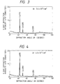
- Fig. 3 is a graph showing a state of crystal of a copper thin film vacuum deposited on the surface of a polyimide film after the surface of the film is irradiated with argon ions under the condition of 2 KeV of accelerating electric field and 3.0 x 10¹⁶/cm2 of dosage,
- Fig. 4 is a graph showing a state of crystal of a copper thin film vacuum deposited on the surface of a polyimide film after the surface of the film is irradiated with argon ions under the condition of 2 KeV of accelerating electric field and 6.0 x 10¹⁶/cm2 of dosage,
- Fig. 5 is a graph showing a relationship of X-ray diffraction intensity per unit film thickness in the (111) face of copper vs. dosage of irradiated ions.
- Fig. 6 is a schematic diagram showing a modification a film forming apparatus for executing the method of forming copper thin film according to the present invention,
- Figs. 7(a) to 7(c) are graphs depicting relationships of X-ray diffraction intensity vs. incident angle of X-rays,
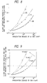
- Fig. 8 is a graph depicting a relationship of X-ray diffraction intensity per unit film thickness vs. irradiated ion dosage, and
- Fig. 9 is a graph showing corrosion resistance of a copper film with respect to X-ray diffraction intensity per unit film thickness and irradiation ion dosage.
-
- Fig. 1 is a diagram roughly showing the construction of an apparatus for forming a copper-film coated substrate according to the present invention. A
holder 2 for holding asubstrate 4 is disposed in a vacuum chamber (not shown). Avapor source 6 and anion source 10 are disposed directed toward theholder 2. - The
vapor source 6 is provided for depositing copper 8 on thesubstrate 4 held by theholder 2. In this instance, copper is heated withelectron beams 7 to evaporate. For the same purpose, copper may be heated by the resistance heating. Further, a target may be sputtered to evaporate copper. - The
ion source 10 acceleratesinert gas ions 12 to expel them toward theholder 2. Thesubstrate 4 on theholder 2 is exposed to the inert gas ions. An ion source of the multi-pole magnetic field type, so-called bucket type, is preferably used because of the large area and large current. As a matter of course, any other ion source may be used for the ion source in the present invention. It is to avoid reaction of irradiated ions with thesubstrate 4 that theinert gas ions 12 are used in this instance. - In this instance, a film thickness monitor 14 and an ion
current monitor 16 are disposed close to theholder 2. The film thickness monitor 14 is for measuring a quantity of copper 8 deposited on thesubstrate 4. The ioncurrent monitor 16 is for measuring a dosage ofinert gas ions 12 applied to thesubstrate 4. - In forming a copper thin film, the desired
substrate 4 on which the film is formed, is attached to theholder 2. A vacuum chamber is evacuated up to a prescribed degree of vacuum (e.g., approximately 1 x 10⁶ Torr). Then, aninert gas 12 is led out of theion source 10, and applied to the surface of thesubstrate 4. Theinert gas ions 12 may be any of helium ions, neon ions, argon ions, krypton ions, and the like. The accelerating energy ofinert gas ions 12 is preferably 100 eV to 20 KeV. The dosage ofinert gas ions 12 is preferably 1.0 x 10¹⁴/cm2 or more. These values actually change depending on the kind ofinert gas ions 12 and material of thesubstrate 4. Accordingly, the best values must be selected for these factors. Thus, the surface of thesubstrate 4 is sputtered by irradiating thesubstrate 4 with theinert gas ions 12. Then, the copper 8 is evaporated from thevapor source 6 and deposited by a desired film thickness on the surface of thesubstrate 4. - To be more specific, a polyimide film was used for the
substrate 4. The surface of the polyimide film was irradiated with argon ions under the condition of 2 KeV of accelerating electric field and 3.0 x 10¹⁶/cm2 or 6.0 x 10¹⁶/cm2 of dosage. The incident angle of argon ions to the film surface was 45°. Cooling water is passed through theholder 2 to cool the polyimide film sufficiently, in order to prevent heat generated with ion irradiation from deforming the polyimide film. Thus, the surface of the polyimide film was sputtered with the inert gas ions. Thereafter, a copper thin film was formed by 1µm thick on the film surface at 10 Å/sec of film forming rate by using thevapor source 6 of the electron beam heating type. For comparison, a copper thin film was formed as in the above manner on the non-treated surface of the polyimide film, which was not exposed to irradiated ions. - A crystal of the copper thin film thus formed on the surface of the polyimide film was analyzed by an X-ray diffraction method to examine its crystallinity. The results of the analysis are shown in Figs. 2 to 4. The result of the analysis when the surface of the substrate is not exposed to irradiated ions is shown in Fig. 2; the result when the substrate surface is irradiated with argon ions of 3.0 x 10¹⁶/cm2 is shown in Fig. 3; and the result when the substrate surface is irradiated with argon ions of 6.0 x 10¹⁶/cm2 is shown in Fig. 4.
- As shown in Fig. 2, in the case where a copper thin film is formed on the surface of the substrate not exposed to irradiated ions, the diffraction peaks are observed at the diffraction angles representing the copper crystal faces of (111), (200), and (220). As seen, the crystal oriented in the (111) face, not large in quantity, exists with mere normal vacuum deposition of copper.
- In the case where, as shown in Fig. 3, after the surface of the polyimide film was irradiated with argon ions of 3.0 x 10¹⁶/cm2, a copper thin film was formed on the film surface, the diffraction peak is remarkably increased in the (111) face of the copper crystal in the copper thin film.
- In the case where, as shown in Fig. 4, after the surface of the polyimide film was irradiated with argon ions of 6.0 x 10¹⁶/cm2, a copper thin film was formed on the film surface, the diffraction peak is further remarkably increased at the (111) face of the copper crystal in the copper thin film. This fact indicates that the crystal oriented in the (111) face has been more greatly formed in the copper thin film.
- As seen from the foregoing description, in the film irradiated with ions, the crystal oriented in the (111) face having the highest density is greatly grown. Further, the growth of the crystal is greater with increase of the irradiated ion dosage.
- Since the X-ray diffraction intensity depends on the thickness of the copper thin film, a variation of X-ray diffraction intensity per unit film thickness in the (111) face with respect to a dosage of argon ions was measured. The result of the measurement is shown in Fig. 5. As shown, as the irradiated ion dosage increases, the X-ray diffraction intensity also increases in the (111) face. From this fact, it is seen that with increase of irradiated ion dosage, the copper crystal oriented in the (111) face is well grown.
- The reason why the crystal is greatly grown in the (111) face when the film surface is exposed to irradiated ions is interpreted as follows. As the result of sputtering the film surface with ions, minute irregularity will be formed in the film surface. With the surface irregularity, the wettability of the film surface is improved, so that formation of the crystal seed of copper has been changed to be favorable to the crystal orientation in the (111) face.
- Thus, the crystal orientation in the (111) face of copper formed on the surface of the substrate can be controlled by exposing the substrate surface to inert gas ions before formation of the copper thin film and by controlling the dosage of inert gas ions. Further, the substrate surface is made irregular by the ion irradiation, so that the crystal can be grown on the substrate independently of the crystal structure and surface state of the substrate.
- The method of exposing the substrate to ions, unlike the method of heating the substrate, is applicable irrespective of the kind of substrate material used. Therefore, the method of the present invention can control the crystal orientation in the (111) face of a thin film formed on the substrate, such as a plastic film and an organic film, which has been considered to be an unsuitable substrate for heating.
- Accordingly, when using the method of the invention, a copper thin film, excellent in corrosion resistance, can be formed on the substrate irrespective of the surface state and the material of the substrate.
- A method of forming a copper thin film according to the present invention is also executed by a film forming apparatus as shown in Fig. 6, which is the same as the apparatus shown in Fig. 1 expect that the incident angle of argon ions to the film surface is 0°.
- The
substrate 4 on which a copper thin film is grown, is located on thesubstrate holder 2. The vacuum chamber is evacuated up to approximately 1 x 10⁻⁶ Torr. Thereafter, in an ion irradiation step thesubstrate 4 is exposed to irradiated ions. In other words, the surface of thesubstrate 4 is irradiated with gas ions generated from theion source 10. The gas ions used here may be any of gas ions of H, N, O, He, Ne, Ar, and Kr. The accelerating energy, irradiated dosage, and irradiation angle depend on the kind of ions and the material of thesubstrate 4. Those are optimumly selected for these factors. Following the ion irradiation step where the surface of thesubstrate 4 is exposed to irradiated ions, a film forming step is executed where copper is evaporated from thevapor source 6, and a copper thin film is formed by a desired thickness on thesubstrate 4. - A crystal of the copper thin film thus formed on the surface of a polyimide film was analyzed by an X-ray diffraction method in order to examine its crystallinity. The results of the analysis are shown in Figs. 7(a) to 7(c). In the figures, the abscissa represents an incident angle of X-rays. The ordinate represents an X-ray diffraction intensity (number of counts x 103 cps). Fig. 7(a) shows the result of the analysis when the surface of the substrate is not exposed to irradiated ions. Fig. 7(b) shows the result of the analysis when the surface of the
substrate 4 is exposed to Ar ions of 1.5 x 10¹⁶/cm2 with irradiaton energy of 2 keV, and a copper thin film is vacuum deposited on thesubstrate 2. When a copper thin film is deposited on the polyimide film of high polymer, for example, ions of argon accelerated by 2 kev are irradiated on the film at 45° of incident angle. In this case, in order to prevent deformation of the polyimide film by heat caused by ion irradiation, cooling water is fed into theholder 2 to sufficiently cool the holder. Subsequently, a copper thin film is formed up to 1 µm thick at 10 Å/sec of film forming rate on the polyimide film surface, that was sputtered with irradiated Ar ions, by an electron beam depositing method. - Fig. 7(c) shows the result of the analysis when the surface of the
substrate 4 is exposed to Ar ions of 1.5 x 10¹⁶/cm2 with irradiaton energy of 5 keV, and then, a copper thin film is vacuum deposited on thesubstrate 4. - As shown in Fig. 7(a), in the case where a copper thin film is formed on the surface of the substrate not exposed to irradiated ions, the diffraction peaks are observed at the diffraction angles representing the copper crystal faces (111), (200), and (220). As seen, the crystal, not large in quantity, has been formed with mere normal vacuum deposition of copper. However, in the case of Fig. 7(b) where the substrate is exposed to Ar ions with the irradiation energy of 2 kev, the diffraction peak is remarkably increased in the (111) face. In the case of Fig. 7(c) where the substrate is exposed to Ar ions of the same quantity as that in the Fig. 7(b) case, but with the irradiation energy of 5 keV, the diffraction peak is further remarkably increased in only the (111) face. This indicates that the copper crystal of the (111) face has been greatly grown on the
substrate 4. In other words, copper tends to be crystallized in the direction of the (111) face on thesubstrate 4 irradiated with Ar ions. - Next, a relationship between X-ray diffraction intensity in the Cu (111) face vs. dosage of irradiated Ar ions, which is shown in Fig. 8, will be considered. In the graph, the abscissa represent a dosage of irradiated Ar ions (ions/cm2). The ordinate represents an X-ray diffraction intensity (1/d (cps/nm)) per unit film thickness. A higher value of the X-ray diffraction intensity indicates that the ratio of crystal in the (111) face is large. Also in the graph, a
curve 100 indicates a variation of X-ray diffraction intensity when Ar ions are accelerated by the energy of 2 keV. Acurve 110 indicates a variation of X-ray diffraction intensity when the ions are accelerated by 5 keV. Acurve 120 indicates a variation of X-ray diffraction intensity when the ions are accelerated by 10 keV. - From Fig. 8, it can be seen that the X-ray diffraction intensity increases with increase of irradiated ion dosage, and that as the irradiation energy is higher, crystal is grown in the direction of the (111) face with a less dosage of irradiated ions. These facts teach us that the growth of copper crystal in the (111) face can be controlled by adjusting the ion irradiation energy and the irradiated ion dosage, and that by increasing the irradiation energy, the crystal can be greatly grown in the (111) face even if the ion dosage is decreased.
- The reason why the crystal is greatly grown in the (111) face when the film surface is exposed to irradiated ions may be interpreted as follows. As described before, as the result of sputtering the film surface with ions, minute irregularity will be formed in the film surface. With the surface irregularity, the wettability of the film surface is improved, so that formation of the crystal seed of copper has been changed to be favorable to the crystal orientation in the (111) face. Further, the number and largeness of the irregularity increases with increase of ion irradiation energy.
- Fig. 9 shows the results of the corrosion resistance test of the copper film thus formed on the polyimide film. In the test, the crystal oriented in the (111) face of copper was controlled by the copper film forming method. Each
substrate 4 was immersed in a solution of hydrochloric acid density 5N for ten minutes. Pin holes in the surface of the copper film were checked by an optical microscope. In the figure, "" indicates that no injury is present; "Δ" indicates that some pin holes are present; "X" indicates that great injury is present.
- As seen from the graph, the substrates of 2.0 (cps/nm) or more in the X-ray diffraction intensity per unit film thickness in the (111) face crystal orientation, have no pin hole and exhibit high corrosion resistance.
- In the present invention, the X-ray diffraction intensity per unit film thickness of copper film is set to be 2.0 (cps/nm) or more in the (111) face crystal orientation. With the selection of a value within such a range, the corrosion resistance of the copper film is improved. Thus, in the etching process and the like, the resultant copper film will not suffer from the pin hole problem and the reduction of the close adhesion of the copper film to the substrate.
- Also, according to the present invention, the crystal orientation in the (111) face of a copper thin film formed on the surface of a substrate by PVD process, can be controlled independently of the crystal structure and surface state of the substrate and without heating the substrate.
- Further, the method of forming a copper thin film of the invention comprises the steps of irradiating the surface of a substrate with ions before a copper thin film is formed thereon, and depositing a copper thin film on the substrate that is irradiated with ions in the ion irradiation step, wherein, in the ion irradiation step, ion irradiation energy for a dosage of irradiated ions is controlled, whereby the crystal is greatly grown in the direction of the (111) face with a less dosage of irradiated ions. Accordingly, the required dosage of irradiated ions is small, and a greater growth of crystal having the crystal orientation in the highest density face can be achieved.
Claims (3)
- A method of forming a copper thin film, comprising the steps of:wherein,irradiating a surface of a substrate with ions having an energy in the range of 2 keV to 10 keV; anddepositing a copper thin film on the substrate that has been irradiated with the ions in the ion irradiating step,
in the ion irradiating step, an ion irradiation energy and/or a dosage of the irradiated ions is controlled, such that the deposited copper film has an X-ray diffraction intensity of 2.0 cps/nm or more per unit film thickness at a crystal orientation (111) face of the copper film. - A method of forming a copper thin film as claimed in ciaim 1,
wherein said substrate is an organic film and said ions are one of H, N, O, He, Ne, Ar and Kr. - A copper film coated substrate, comprising:characterized in thata substrate; anda copper film formed on a surface of said substrate, said copper film having an X-ray diffraction intensity of 2.0 cps/nm or more per unit film thickness at a crystal orientation (111) face of said copper film,
said substrate is an organic film.
Applications Claiming Priority (9)
| Application Number | Priority Date | Filing Date | Title |
|---|---|---|---|
| JP70389/92 | 1992-02-20 | ||
| JP07038992A JP3227768B2 (en) | 1992-02-20 | 1992-02-20 | Method for controlling crystal orientation of copper thin film |
| JP7038992 | 1992-02-20 | ||
| JP6623992A JPH05271902A (en) | 1992-03-24 | 1992-03-24 | Formation of thin cu film |
| JP66239/92 | 1992-03-24 | ||
| JP6623992 | 1992-03-24 | ||
| JP84299/92 | 1992-04-07 | ||
| JP8429992 | 1992-04-07 | ||
| JP8429992A JPH05287506A (en) | 1992-04-07 | 1992-04-07 | Copper film-coated substrate |
Publications (3)
| Publication Number | Publication Date |
|---|---|
| EP0565766A2 EP0565766A2 (en) | 1993-10-20 |
| EP0565766A3 EP0565766A3 (en) | 1995-08-23 |
| EP0565766B1 true EP0565766B1 (en) | 2002-04-24 |
Family
ID=27299060
Family Applications (1)
| Application Number | Title | Priority Date | Filing Date |
|---|---|---|---|
| EP19920109570 Expired - Lifetime EP0565766B1 (en) | 1992-02-20 | 1992-06-05 | Copper film coated substrate and method of forming copper film on substrate |
Country Status (3)
| Country | Link |
|---|---|
| US (2) | US5316802A (en) |
| EP (1) | EP0565766B1 (en) |
| DE (1) | DE69232575T2 (en) |
Families Citing this family (14)
| Publication number | Priority date | Publication date | Assignee | Title |
|---|---|---|---|---|
| US5686733A (en) * | 1996-03-29 | 1997-11-11 | Mcgill University | Megavoltage imaging method using a combination of a photoreceptor with a high energy photon converter and intensifier |
| US6197134B1 (en) | 1997-01-08 | 2001-03-06 | Dowa Mining Co., Ltd. | Processes for producing fcc metals |
| JP3403918B2 (en) * | 1997-06-02 | 2003-05-06 | 株式会社ジャパンエナジー | High purity copper sputtering target and thin film |
| GB2331765A (en) | 1997-12-01 | 1999-06-02 | Cambridge Display Tech Ltd | Sputter deposition onto organic material using neon as the discharge gas |
| US6140235A (en) * | 1997-12-05 | 2000-10-31 | Applied Materials, Inc. | High pressure copper fill at low temperature |
| US6632292B1 (en) * | 1998-03-13 | 2003-10-14 | Semitool, Inc. | Selective treatment of microelectronic workpiece surfaces |
| US6331490B1 (en) * | 1998-03-13 | 2001-12-18 | Semitool, Inc. | Process for etching thin-film layers of a workpiece used to form microelectric circuits or components |
| US6149776A (en) * | 1998-11-12 | 2000-11-21 | Applied Materials, Inc. | Copper sputtering target |
| US6605321B1 (en) * | 2000-07-20 | 2003-08-12 | Centre National De La Recherche Scientifique (Cnrs) | Method of treating materials by irradiation |
| US6495436B2 (en) * | 2001-02-09 | 2002-12-17 | Micron Technology, Inc. | Formation of metal oxide gate dielectric |
| KR20040026733A (en) * | 2002-09-25 | 2004-04-01 | 주식회사 피앤아이 | Method and Apparatus for Formation of Thick Layer on the Surface Modified Substrate |
| US7077889B2 (en) * | 2003-04-04 | 2006-07-18 | Intelligent Engery, Inc. | Surface modification of porous metal substrates |
| JP5352542B2 (en) * | 2010-07-15 | 2013-11-27 | エル エス エムトロン リミテッド | Copper foil for current collector of lithium secondary battery |
| US10147697B1 (en) | 2017-12-15 | 2018-12-04 | Nxp Usa, Inc. | Bond pad structure for semiconductor device packaging |
Family Cites Families (12)
| Publication number | Priority date | Publication date | Assignee | Title |
|---|---|---|---|---|
| FR1547700A (en) * | 1967-10-18 | 1968-11-29 | Comp Generale Electricite | Improved adhesion of metal deposits on a surface made of a synthetic material |
| US4086082A (en) * | 1976-04-16 | 1978-04-25 | Shalom Mahalla | Copper crystal and process |
| US4720401A (en) * | 1985-01-11 | 1988-01-19 | International Business Machines Corporation | Enhanced adhesion between metals and polymers |
| JP2597352B2 (en) * | 1985-06-20 | 1997-04-02 | インターナショナル・ビジネス・マシーンズ・コーポレーション | Method for improving adhesion between metal and organic substrate |
| JPH079069B2 (en) * | 1986-03-12 | 1995-02-01 | ブラザー工業株式会社 | Method for forming copper coating with excellent mechanical properties |
| US4695348A (en) * | 1986-09-15 | 1987-09-22 | Psi Star | Copper etching process and product |
| US4886681A (en) * | 1987-01-20 | 1989-12-12 | International Business Machines Corporation | Metal-polymer adhesion by low energy bombardment |
| JPS6475663A (en) * | 1987-09-17 | 1989-03-22 | Kobe Steel Ltd | Cu plated material having high corrosion resistance and production thereof |
| GB8817664D0 (en) * | 1988-07-25 | 1988-09-01 | Ici Plc | Polymeric films |
| US5087476A (en) * | 1989-03-17 | 1992-02-11 | Matsushita Electric Industrial Co., Ltd. | Method of producing thin film |
| US4975327A (en) * | 1989-07-11 | 1990-12-04 | Minnesota Mining And Manufacturing Company | Polyimide substrate having a textured surface and metallizing such a substrate |
| JP3413181B2 (en) * | 2001-08-03 | 2003-06-03 | 川崎重工業株式会社 | Continuous hot rolling equipment |
-
1992
- 1992-06-04 US US07/892,378 patent/US5316802A/en not_active Expired - Lifetime
- 1992-06-05 DE DE69232575T patent/DE69232575T2/en not_active Expired - Fee Related
- 1992-06-05 EP EP19920109570 patent/EP0565766B1/en not_active Expired - Lifetime
-
1993
- 1993-05-25 US US08/065,913 patent/US5501911A/en not_active Expired - Lifetime
Also Published As
| Publication number | Publication date |
|---|---|
| EP0565766A2 (en) | 1993-10-20 |
| US5501911A (en) | 1996-03-26 |
| DE69232575T2 (en) | 2002-08-08 |
| DE69232575D1 (en) | 2002-05-29 |
| US5316802A (en) | 1994-05-31 |
| EP0565766A3 (en) | 1995-08-23 |
Similar Documents
| Publication | Publication Date | Title |
|---|---|---|
| US5316802A (en) | Method of forming copper film on substrate | |
| Marinov | Effect of ion bombardment on the initial stages of thin film growth | |
| Sonnenberg et al. | Preparation of biaxially aligned cubic zirconia films on pyrex glass substrates using ion‐beam assisted deposition | |
| EP0269111A2 (en) | Method of forming a thin aluminium film | |
| US6787441B1 (en) | Method for pretreating a polymer substrate using an ion beam for subsequent deposition of indium oxide or indium tin oxide | |
| US20040083969A1 (en) | Film forming apparatus, substrate for forming oxide thin film, and production method thereof | |
| DE68925459T2 (en) | Process for the production of thin layers of metastable binary compounds | |
| JP3227795B2 (en) | Method for controlling crystal orientation of aluminum film | |
| US5679625A (en) | Method of making an oxide superconducting thin film | |
| Yamada et al. | Film and interface properties of epitaxial metal/insulator/semiconductor systems formed by ionized cluster beam deposition | |
| US5496772A (en) | Method of manufacturing film carrier type substrate | |
| EP0486054B1 (en) | Process for preparing a superconducting thin oxide film | |
| JP3227768B2 (en) | Method for controlling crystal orientation of copper thin film | |
| DE3874165T2 (en) | METHOD FOR PRODUCING A DIAMOND LAYER. | |
| US5523166A (en) | Process for forming thin film having excellent insulating property and metallic substrate coated with insulating material formed by said process | |
| Masato et al. | Microstructure of titanium nitride films produced by the dynamic mixing method | |
| Kuratani et al. | Influences of ion energy on morphology and preferred orientation of chromium thin films prepared by ion beam and vapor deposition | |
| JPH05287506A (en) | Copper film-coated substrate | |
| JPH04337445A (en) | Speculum sample preparation method | |
| Noggle | The preparation and characterization of single crystal silver films | |
| Min et al. | Ion-assisted crystal growth by post irradiation as applied to nitride formation | |
| KR102579090B1 (en) | Ion Beam Sputtering Apparatus for Manufacturing a Wire Grid Polarizer | |
| JPH05271902A (en) | Formation of thin cu film | |
| US5124174A (en) | Process for forming one or more substantially pure layers in substrate material using ion implantation | |
| JPH0663087B2 (en) | Method for forming titanium nitride film |
Legal Events
| Date | Code | Title | Description |
|---|---|---|---|
| PUAI | Public reference made under article 153(3) epc to a published international application that has entered the european phase |
Free format text: ORIGINAL CODE: 0009012 |
|
| AK | Designated contracting states |
Kind code of ref document: A2 Designated state(s): DE FR GB |
|
| PUAL | Search report despatched |
Free format text: ORIGINAL CODE: 0009013 |
|
| AK | Designated contracting states |
Kind code of ref document: A3 Designated state(s): DE FR GB |
|
| 17P | Request for examination filed |
Effective date: 19951127 |
|
| 17Q | First examination report despatched |
Effective date: 19980729 |
|
| GRAG | Despatch of communication of intention to grant |
Free format text: ORIGINAL CODE: EPIDOS AGRA |
|
| GRAG | Despatch of communication of intention to grant |
Free format text: ORIGINAL CODE: EPIDOS AGRA |
|
| GRAH | Despatch of communication of intention to grant a patent |
Free format text: ORIGINAL CODE: EPIDOS IGRA |
|
| REG | Reference to a national code |
Ref country code: GB Ref legal event code: IF02 |
|
| GRAH | Despatch of communication of intention to grant a patent |
Free format text: ORIGINAL CODE: EPIDOS IGRA |
|
| GRAA | (expected) grant |
Free format text: ORIGINAL CODE: 0009210 |
|
| AK | Designated contracting states |
Kind code of ref document: B1 Designated state(s): DE FR GB |
|
| REG | Reference to a national code |
Ref country code: GB Ref legal event code: FG4D |
|
| REF | Corresponds to: |
Ref document number: 69232575 Country of ref document: DE Date of ref document: 20020529 |
|
| PGFP | Annual fee paid to national office [announced via postgrant information from national office to epo] |
Ref country code: FR Payment date: 20020627 Year of fee payment: 11 |
|
| PGFP | Annual fee paid to national office [announced via postgrant information from national office to epo] |
Ref country code: DE Payment date: 20020729 Year of fee payment: 11 |
|
| ET | Fr: translation filed | ||
| PLBE | No opposition filed within time limit |
Free format text: ORIGINAL CODE: 0009261 |
|
| STAA | Information on the status of an ep patent application or granted ep patent |
Free format text: STATUS: NO OPPOSITION FILED WITHIN TIME LIMIT |
|
| 26N | No opposition filed |
Effective date: 20030127 |
|
| PG25 | Lapsed in a contracting state [announced via postgrant information from national office to epo] |
Ref country code: DE Free format text: LAPSE BECAUSE OF NON-PAYMENT OF DUE FEES Effective date: 20040101 |
|
| PG25 | Lapsed in a contracting state [announced via postgrant information from national office to epo] |
Ref country code: FR Free format text: LAPSE BECAUSE OF NON-PAYMENT OF DUE FEES Effective date: 20040227 |
|
| REG | Reference to a national code |
Ref country code: FR Ref legal event code: ST |
|
| PGFP | Annual fee paid to national office [announced via postgrant information from national office to epo] |
Ref country code: GB Payment date: 20070530 Year of fee payment: 16 |
|
| GBPC | Gb: european patent ceased through non-payment of renewal fee |
Effective date: 20080605 |
|
| PG25 | Lapsed in a contracting state [announced via postgrant information from national office to epo] |
Ref country code: GB Free format text: LAPSE BECAUSE OF NON-PAYMENT OF DUE FEES Effective date: 20080605 |