EP0563491A1 - Verfahren und Vorrichtung zur Ausführung eines Kodes, der Dreifachfehler erkennt und Zweifachfehler korrigiert - Google Patents
Verfahren und Vorrichtung zur Ausführung eines Kodes, der Dreifachfehler erkennt und Zweifachfehler korrigiert Download PDFInfo
- Publication number
- EP0563491A1 EP0563491A1 EP92480054A EP92480054A EP0563491A1 EP 0563491 A1 EP0563491 A1 EP 0563491A1 EP 92480054 A EP92480054 A EP 92480054A EP 92480054 A EP92480054 A EP 92480054A EP 0563491 A1 EP0563491 A1 EP 0563491A1
- Authority
- EP
- European Patent Office
- Prior art keywords
- error
- matrix
- bit
- bits
- rows
- Prior art date
- Legal status (The legal status is an assumption and is not a legal conclusion. Google has not performed a legal analysis and makes no representation as to the accuracy of the status listed.)
- Ceased
Links
Images

Classifications
-
- H—ELECTRICITY
- H03—ELECTRONIC CIRCUITRY
- H03M—CODING; DECODING; CODE CONVERSION IN GENERAL
- H03M13/00—Coding, decoding or code conversion, for error detection or error correction; Coding theory basic assumptions; Coding bounds; Error probability evaluation methods; Channel models; Simulation or testing of codes
- H03M13/03—Error detection or forward error correction by redundancy in data representation, i.e. code words containing more digits than the source words
- H03M13/05—Error detection or forward error correction by redundancy in data representation, i.e. code words containing more digits than the source words using block codes, i.e. a predetermined number of check bits joined to a predetermined number of information bits
- H03M13/13—Linear codes
- H03M13/15—Cyclic codes, i.e. cyclic shifts of codewords produce other codewords, e.g. codes defined by a generator polynomial, Bose-Chaudhuri-Hocquenghem [BCH] codes
- H03M13/151—Cyclic codes, i.e. cyclic shifts of codewords produce other codewords, e.g. codes defined by a generator polynomial, Bose-Chaudhuri-Hocquenghem [BCH] codes using error location or error correction polynomials
Definitions
- the subject invention relates to a method and an apparatus for achieving the detection of triple errors and the correction of double errors in data stored in a memory or processed in a data processing system, said method and apparatus being based on a modification of a standard Bose Chauduri Hocquenghem BCH code that permits a reduction of the decoding circuitry needed to achieve the detection and correction of the errors.
- Bose Chaudri Hocquenghem BCH codes are based on the GALOIS field theory.
- a Galois field is a finite collection of binary elements generated from an irreducible polynomial.
- a list of irreducible polynomials can be found in the book "Error Correcting Codes" by Peterson and Weldon, the MIT press, Second Edition 1972, for instance.
- the first row is an all 1 row. It is added to enhance the code to the detection of all triple errors, otherwise there will be no way to make a difference between a double and a triple error.
- the method according to the present invention implements a triple error detection/double error correction code in a m-bit word comprising data bits and error correction code ECC bits.
- the method comprises the steps of:
- the analyzing step is made by:
- the method also comprises the following steps:
- the bits found in error are inverted for correcting them and generating a corrected word.
- the subject invention also relates to the apparatus for implementing said method.
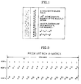
- Figure 1 represents the set of 15 elements of a Galois field generated from an irreducible polynomial of degree 4.
- Figure 2 represents the addition table for the elements of the Galois field shown in Figure 1.
- Figure 3 represents a prior art BCH matrix.
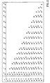
- Figure 4 and 6 represents the modified matrix H according to the subject invention.
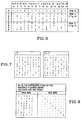
- Figure 5 represents a correspondence table between the shortest distance d, the product SaxSb and a value E to be used for detecting the position of two bits in error.
- Figure 7 represents the matrices T and T ⁇ 1 used for generating the systematic form H1 shown in Figure 8 of the matrix H.
- Figure 9 represents which conditions are met when a single bit error, double bit error or triple bit error has occurred.
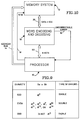
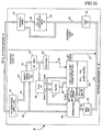
- Figure 10 represents the block diagram of the apparatus of the present invention when implemented to code the words to be stored into a memory and decode and correct the words read from the memory.
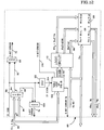
- FIG. 11 represents the apparatus of the present invention in more details.
- Figure 12 represents the error detection and error position computation circuit shown as 68 in Figure 11.
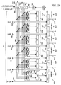
- Figure 13 represents the error correction circuit shown as 80 in Figure 12.
- Double Error Correction/Triple Error Detection code is based on a modified Bose Chauduri Hocquenghem matrix shown in Figure 3.
- the row 0 and row a are identical to the row 0 and a of the prior art matrix, but the row b is changed as shown in Figure 3.
- Figure 6 represents the modified H-matrix of figure 4 wherein each element ⁇ has been replaced by its binary value shown in Figure 1.
- the data words are encoded in such a way that a parity bit is included in selected fields of the data words so that the selected fields have an odd parity for example, the selected fields are defined by the "1" in the matrix of figure 6.
- the first selected field of a 15-bit words comprises the 15 bits
- the second selected field is defined by the second row and comprises bits in position 0, 4, 7, 8, 10, 12, 13, 14.
- the third selected field is defined by the third row, etc.
- E and d are calculated using the addition table shown in Figure 2.
- a memory word Before being stored, a memory word must be encoded using the modified matrix H shown in Figure 6. However, the matrix cannot be used as is to encode the words to be stored. It must be transformed into its systematic form H1 to permit the computation of the Error Correcting Code ECC bits added to the data bits coming from the processor into which the memory is incorporated.
- the systematic form of the modified matrix H is shown in Figure 8.
- the nine most right columns correspond to the ECC bits to be computed from the 6 data bits before storing a word. Again this is an example, there is no practical application for it, since 9 ECC bits would have to be added to 6 data bits only. From the teaching of this example, the man skilled in the art would be able to implement the subject invention, by determining the set of elements of a Galois field generated from an irreducible polynomial of a higher degree and encoding the words using a matrix comprising the elements so determined and having the same property as the modified matrix shown in Figure 4.
- H1 is an odd weigh matrix, which means that the number of 1 in each column is odd , the parity of the error syndrome S1 generated upon reading of a word from the memory, indicates if a single, double or triple error has occurred.
- An odd syndrome S1 is indicative of a single or triple error, while an even syndrome S1 is indicative of a double error.
- bit positions in error can be found by computing d, ⁇ ai and ⁇ aj as described above.
- Figure 10 represents a logic implementation allowing to implement the encoding of the words to be stored in a memory and the decoding and the words read from the memory.
- the processor 10 accesses the memory 12, though address bus and a read/write control signal on line 16.
- the word read from the addressed memory location comprising the data and ECC bits are provided to the logic circuit 18 through bus 20.
- Logic circuit 18 decodes the word and if no error, a single bit error or a double bit error is detected, provides the data bits corrected if necessary to the processor through bus 22. If a three bit uncorrectable error is detected, a three-bit error signal is provided to the processor through line 19.
- the data bits are provided by the processor to logic circuit 18 through bus 22, and are encoded to provide the data bits and ECC bits to the memory through bus 20.
- the logic circuit 18 is represented in Figure 11.
- Logic circuit 18 comprise an encoding logic 30 and a decoding logic 32.
- the data to be written into the memory are received by the encoding logic into data-in register 34, and provided to an ECC bit generation circuit 36, which computes the ECC bits to be added to the data bits so that the parity of the fields determined by the 1 in the rows of matrix H1 is odd. Obviously, an even parity might also be used.
- the ECC bits generated on bus 38 and the data bits from bus 35 are provided into register 40 as the encoded word to be written into the memory through bus 20.
- a word fetched from the memory is provided into register 42 from bus 20.
- the ECC bits and data bits are provided to parity check circuit 44 through bus 46 and 48.
- Parity check circuit 44 checks the parity of the fields of data and check bits determined by the matrix H1 to generate the error syndrome S1 on its output bus 50.
- the syndrome S1 is stored into register 52.
- Syndrome S1 is provided to ODD/EVEN detection logic and to multiplier circuit 56.
- ODD/EVEN detection logic detects whether the syndrome S1 has an even or odd parity and generates a 1 level signal on line 58 if the parity is odd, which is indicative of a single bit error or triple bit error.
- the multiplier circuit 56 multiplies the syndrome S1 by matrix T to retrieve the S syndrome, which would have been found if the matrix H were used instead of matrix H1.
- syndrome S is comprised of sub-syndromes S0, Sa, Sb. Sa and Sb are provided to multiplier circuit 60 through bus 62 and 64.
- the ⁇ ai and ⁇ aj values are provided to correction logic circuit 80 through bus 76 and 78 together with the signals on lines 72 and 74 and Sa on bus 62.
- Circuit 68 will be described in more details in reference to figure 12.
- Correction circuit 80 which will be described in reference to figure 14, receives the data bits and correct them if needed, and provide the data bits corrected or not, to data out register 82 through bus 84.
- the data bits in register 82 are available to the processor.
- the error detection and ⁇ ai and ⁇ aj computation circuit 68 is shown in Figure 12.
- the S1 ODD line 58 is provided to the first input of an AND circuit 90, which receives on its second input 92 a signal at a "1' level provided by comparator 94.
- Comparator 92 compares the SaxSb product from bus 66 with the value on bus 96. It generates a "1" level signal on its output line 92 when an inequality is detected an a "1" level signal on its output line 98 when an equality is detected.
- AND gate 90 provides a 3-bit error signal at a "1" level on its output line 70 when S1 is odd and SaxSb is different from ⁇ 0.
- Lines 58 and 98 are provided to the inputs of an AND gate 100 which generates a 1-bit error signal at a "1" level on its output line 74 when S1 is odd and SAxSb is equal to ⁇ 0.
- the signal on line 58 is provided to an inverter 102 which generates on its output line 104 a signal at a "1" level when S1 is even.
- This signal activates a table look up circuit 106 which receives the product SaXSb from bus 66 and generates the values E and d on its output busses 108 and 110 respectively, according to the correspondences shown in Figure 5.
- the correction circuit 80 is shown in Figure 13.
- the correction circuit comprises XOR circuits 130, 131, 132, 133, 134 and 135 which receive the data bits 0 to 5 read from bus 48 on a first input (136 to 142) and an invert control signal on a second output (143 to 148).
- the invert control signal is provided by logic circuits 150 to 155.
- the position of the bit in error in case a 1-bit error is detected is indicated by Sa and the positions of the two bits in error in case a 2-bit error is detected are indicated by ⁇ ai and ⁇ aj.
- signal on line 74 is at a "1" level. This signal is provided to the input of inverter 156, the output line 158 of which is provided to AND gate 160.
- the 1-bit error line 74 and 2-bit error line 72 are provided a multiplex circuit 166, which receives as inputs the subsyndrome Sa from bus 62 and the ⁇ ai value from bus 78, and gates on its output bus the Sa value is the 1-bit error signal is active and the ⁇ ai value if the 2-bit error signal is active.
- ⁇ aj from bus 78 is provided to the inputs of AND gate 160.
- multiplex circuit 166 provides Sa on its output bus 168 and AND gate 160 provides 0000 on its output bus 170.
- multiplex circuit 166 provides ⁇ ai on its output bus 168 and AND gate 160 provides ⁇ aj on its output bus 170.
- Each circuit 150 to 155 comprises two AND gates 180 and 182 the output lines of which are provided to the inputs of an OR gate 184.
- OR gate 184 provides the invert control signal on its output line.
- AND gate 180 The inputs of AND gate 180 are connected to bus 168 and the inputs of AND gates 182 are connected to bus 170.
- each AND gate 180 and 182 in circuit 150 to 155 is able to provide a signal at a "1' level on its output when it detects that the values on their inputs correspond to the ⁇ ai value and possibly to the ⁇ aj value (in case of a 2-bit error) at the corresponding column 0 to 5 in the matrix shown in Figure 6.
- AND gate 180 in circuit 150 provides a "1" level output signal to the input of OR circuit 184
- AND gate 182 in circuit 154 provides a "1" level output signal to the input of OR circuit 184, so that an invert control signal is generated on line 143 and 147 which causes bits 0 and 4 to be inverted by XOR circuit 130 and 134 and inverted bits to be provided on their output lines 200 and 204.
- the other circuits 131, 132, 133 and 135 provides the bits 1, 2, 3 and 5 on their output lines 201, 202, 203, 205.
- the code has the capability of detecting error of higher rank, by decoding through table look up circuit 106 that the syndrome S1 is even and that the SaxSb product is different from the values indicated in Figure 5, namely: ⁇ 0, ⁇ 5, ⁇ 7, ⁇ 10, ⁇ 11, or ⁇ 14, and generating a 4-bit error signal on line 210 which corresponds to an uncorrectable error.
Landscapes
- Physics & Mathematics (AREA)
- Mathematical Physics (AREA)
- Algebra (AREA)
- General Physics & Mathematics (AREA)
- Pure & Applied Mathematics (AREA)
- Probability & Statistics with Applications (AREA)
- Engineering & Computer Science (AREA)
- Theoretical Computer Science (AREA)
- Error Detection And Correction (AREA)
- Detection And Correction Of Errors (AREA)
Priority Applications (2)
| Application Number | Priority Date | Filing Date | Title |
|---|---|---|---|
| EP92480054A EP0563491A1 (de) | 1992-03-31 | 1992-03-31 | Verfahren und Vorrichtung zur Ausführung eines Kodes, der Dreifachfehler erkennt und Zweifachfehler korrigiert |
| US07/981,155 US5459740A (en) | 1992-03-31 | 1992-11-23 | Method and apparatus for implementing a triple error detection and double error correction code |
Applications Claiming Priority (1)
| Application Number | Priority Date | Filing Date | Title |
|---|---|---|---|
| EP92480054A EP0563491A1 (de) | 1992-03-31 | 1992-03-31 | Verfahren und Vorrichtung zur Ausführung eines Kodes, der Dreifachfehler erkennt und Zweifachfehler korrigiert |
Publications (1)
| Publication Number | Publication Date |
|---|---|
| EP0563491A1 true EP0563491A1 (de) | 1993-10-06 |
Family
ID=8211783
Family Applications (1)
| Application Number | Title | Priority Date | Filing Date |
|---|---|---|---|
| EP92480054A Ceased EP0563491A1 (de) | 1992-03-31 | 1992-03-31 | Verfahren und Vorrichtung zur Ausführung eines Kodes, der Dreifachfehler erkennt und Zweifachfehler korrigiert |
Country Status (2)
| Country | Link |
|---|---|
| US (1) | US5459740A (de) |
| EP (1) | EP0563491A1 (de) |
Cited By (2)
| Publication number | Priority date | Publication date | Assignee | Title |
|---|---|---|---|---|
| US7103824B2 (en) * | 2002-07-29 | 2006-09-05 | Robert Halford | Multi-dimensional data protection and mirroring method for micro level data |
| CN109347489A (zh) * | 2018-11-23 | 2019-02-15 | 清华大学 | 一种用于通信的基于图形处理器的bch码并行译码方法 |
Families Citing this family (13)
| Publication number | Priority date | Publication date | Assignee | Title |
|---|---|---|---|---|
| US5802078A (en) * | 1992-11-27 | 1998-09-01 | Kokusai Electric Co., Ltd. | Error detector for error detecting codes |
| US6041430A (en) * | 1997-11-03 | 2000-03-21 | Sun Microsystems, Inc. | Error detection and correction code for data and check code fields |
| US7430167B2 (en) * | 2003-09-18 | 2008-09-30 | International Business Machines Corporation | Method and system to enable an adaptive load balancing in a parallel packet switch |
| US7562283B2 (en) * | 2005-12-27 | 2009-07-14 | D.S.P. Group Ltd. | Systems and methods for error correction using binary coded hexidecimal or hamming decoding |
| JP4846384B2 (ja) * | 2006-02-20 | 2011-12-28 | 株式会社東芝 | 半導体記憶装置 |
| JP4836608B2 (ja) * | 2006-02-27 | 2011-12-14 | 株式会社東芝 | 半導体記憶装置 |
| JP2007305267A (ja) * | 2006-05-15 | 2007-11-22 | Toshiba Corp | 半導体記憶装置 |
| JP4891704B2 (ja) * | 2006-08-28 | 2012-03-07 | 株式会社東芝 | 半導体記憶装置 |
| US8108759B2 (en) * | 2006-12-14 | 2012-01-31 | Regents Of The University Of Minnesota | Error detection and correction using error pattern correcting codes |
| JP5259343B2 (ja) * | 2008-10-31 | 2013-08-07 | 株式会社東芝 | メモリ装置 |
| DE102013215055B4 (de) * | 2013-07-31 | 2021-01-28 | Infineon Technologies Ag | Schaltungsanordnung, Vorrichtung, Verfahren und Computerprogramm mit modifiziertem Fehlersyndrom zur Fehlererkennung von permanenten Fehlern in Speichern |
| US20150067437A1 (en) * | 2013-08-30 | 2015-03-05 | Kuljit S. Bains | Apparatus, method and system for reporting dynamic random access memory error information |
| US20170324425A1 (en) * | 2016-05-06 | 2017-11-09 | Infineon Technologies Ag | Embedded parity matrix generator |
Citations (4)
| Publication number | Priority date | Publication date | Assignee | Title |
|---|---|---|---|---|
| EP0204576A2 (de) * | 1985-06-07 | 1986-12-10 | Sony Corporation | Anordnung und Verfahren zur Dekodierung eines BCH-Kodes |
| EP0316063A2 (de) * | 1987-11-10 | 1989-05-17 | International Business Machines Corporation | Nachschlagetabellen verwendende Fehlerkorrektur |
| US4856004A (en) * | 1987-10-05 | 1989-08-08 | Motorola, Inc. | Microprocessor based BCH decoder |
| EP0341862A2 (de) * | 1988-05-12 | 1989-11-15 | Quantum Corporation | Fehlerortungssystem |
Family Cites Families (9)
| Publication number | Priority date | Publication date | Assignee | Title |
|---|---|---|---|---|
| US4509172A (en) * | 1982-09-28 | 1985-04-02 | International Business Machines Corporation | Double error correction - triple error detection code |
| US4556977A (en) * | 1983-09-15 | 1985-12-03 | International Business Machines Corporation | Decoding of BCH double error correction - triple error detection (DEC-TED) codes |
| US4747103A (en) * | 1985-03-21 | 1988-05-24 | Canon Kabushiki Kaisha | Signal processing apparatus for correcting decoding errors |
| US4703485A (en) * | 1986-02-10 | 1987-10-27 | International Business Machines Corporation | Method and apparatus for computing and implementing error detection check bytes |
| US4890286A (en) * | 1987-12-11 | 1989-12-26 | Sanyo Electric Co., Ltd. | Method and apparatus for decoding error correcting code |
| EP0339166B1 (de) * | 1988-04-29 | 1993-07-07 | International Business Machines Corporation | Ausgebreitete Fehlerkorrekturvorrichtung mit Einzel-Paket-Fehlerkorrektur und Doppel-Paket-Fehlerdetektionscoden |
| JPH02125532A (ja) * | 1988-11-04 | 1990-05-14 | Sony Corp | Bch符号の復号装置 |
| US5040179A (en) * | 1989-08-18 | 1991-08-13 | Loral Aerospace Corp. | High data rate BCH encoder |
| JPH03179923A (ja) * | 1989-12-08 | 1991-08-05 | Matsushita Electric Ind Co Ltd | Bch符号の復号方法および装置 |
-
1992
- 1992-03-31 EP EP92480054A patent/EP0563491A1/de not_active Ceased
- 1992-11-23 US US07/981,155 patent/US5459740A/en not_active Expired - Fee Related
Patent Citations (4)
| Publication number | Priority date | Publication date | Assignee | Title |
|---|---|---|---|---|
| EP0204576A2 (de) * | 1985-06-07 | 1986-12-10 | Sony Corporation | Anordnung und Verfahren zur Dekodierung eines BCH-Kodes |
| US4856004A (en) * | 1987-10-05 | 1989-08-08 | Motorola, Inc. | Microprocessor based BCH decoder |
| EP0316063A2 (de) * | 1987-11-10 | 1989-05-17 | International Business Machines Corporation | Nachschlagetabellen verwendende Fehlerkorrektur |
| EP0341862A2 (de) * | 1988-05-12 | 1989-11-15 | Quantum Corporation | Fehlerortungssystem |
Non-Patent Citations (2)
| Title |
|---|
| INTERNATIONAL JOURNAL OF ELECTRONICS vol. 64, no. 4, April 1988, LONDON GB pages 637 - 640 KATSAROS 'Decoding of the (15,7) and (31,21) binary BCH codes' * |
| PATENT ABSTRACTS OF JAPAN vol. 4, no. 31 (P-2)18 March 1980 & JP-A-55 004 623 ( KOKUSAI ELECTRIC CO LTD ) 14 January 1980 * |
Cited By (3)
| Publication number | Priority date | Publication date | Assignee | Title |
|---|---|---|---|---|
| US7103824B2 (en) * | 2002-07-29 | 2006-09-05 | Robert Halford | Multi-dimensional data protection and mirroring method for micro level data |
| CN109347489A (zh) * | 2018-11-23 | 2019-02-15 | 清华大学 | 一种用于通信的基于图形处理器的bch码并行译码方法 |
| CN109347489B (zh) * | 2018-11-23 | 2021-07-27 | 清华大学 | 一种用于通信的基于图形处理器的bch码并行译码方法 |
Also Published As
| Publication number | Publication date |
|---|---|
| US5459740A (en) | 1995-10-17 |
Similar Documents
| Publication | Publication Date | Title |
|---|---|---|
| US7278085B1 (en) | Simple error-correction codes for data buffers | |
| US4030067A (en) | Table lookup direct decoder for double-error correcting (DEC) BCH codes using a pair of syndromes | |
| US5418796A (en) | Synergistic multiple bit error correction for memory of array chips | |
| EP0107038B1 (de) | Kode für Speicher mit Zweifachfehlerkorrektur und Dreifachfehlerdetektion | |
| US6041430A (en) | Error detection and correction code for data and check code fields | |
| US4402045A (en) | Multi-processor computer system | |
| US6604222B1 (en) | Block code to efficiently correct adjacent data and/or check bit errors | |
| Kaneda et al. | Single Byte Error Correcting—Double Byte Error Detecting Codes for Memory Systems | |
| US5459740A (en) | Method and apparatus for implementing a triple error detection and double error correction code | |
| US5251219A (en) | Error detection and correction circuit | |
| US8694872B2 (en) | Extended bidirectional hamming code for double-error correction and triple-error detection | |
| US8806295B2 (en) | Mis-correction and no-correction rates for error control | |
| EP0147336B1 (de) | Fehlerkorrektur- und Detektionssystem | |
| JP2000134111A (ja) | 単一ビットのエラ―を訂正し、対になった二重ビットのエラ―を検出する装置と方法 | |
| EP0793174B1 (de) | Verfahren und Einrichtung zum Nachweis und zur Korrektur von Computerspeicherfehlern | |
| US3688265A (en) | Error-free decoding for failure-tolerant memories | |
| US8694850B1 (en) | Fast erasure decoding for product code columns | |
| US7093183B2 (en) | Symbol level error correction codes which protect against memory chip and bus line failures | |
| EP0629051A1 (de) | Fehlerkorrekturgerät für digitale Daten zur Korrektur von Einfachfehlern (sec), von Doppelfehlern (ded) und Vielfacheinzelbytefehlern (sbd) und zur Korrektur von Einzelbytefehlern ungerader Anzahl (odd sbc) | |
| US5491702A (en) | Apparatus for detecting any single bit error, detecting any two bit error, and detecting any three or four bit error in a group of four bits for a 25- or 64-bit data word | |
| US3766521A (en) | Multiple b-adjacent group error correction and detection codes and self-checking translators therefor | |
| US6772390B2 (en) | Erasure correction for ECC entities | |
| US20150007000A1 (en) | Additional Error Correction Apparatus and Method | |
| JP2732862B2 (ja) | データ伝送試験装置 | |
| Rubinoff | n-dimensional codes for detecting and correcting multiple errors0 |
Legal Events
| Date | Code | Title | Description |
|---|---|---|---|
| PUAI | Public reference made under article 153(3) epc to a published international application that has entered the european phase |
Free format text: ORIGINAL CODE: 0009012 |
|
| AK | Designated contracting states |
Kind code of ref document: A1 Designated state(s): DE FR GB |
|
| 17P | Request for examination filed |
Effective date: 19931227 |
|
| 17Q | First examination report despatched |
Effective date: 19951110 |
|
| STAA | Information on the status of an ep patent application or granted ep patent |
Free format text: STATUS: THE APPLICATION HAS BEEN REFUSED |
|
| 18R | Application refused |
Effective date: 19960502 |