EP0561497B1 - Surface mount electrical connector and shield therefor - Google Patents
Surface mount electrical connector and shield therefor Download PDFInfo
- Publication number
- EP0561497B1 EP0561497B1 EP93300980A EP93300980A EP0561497B1 EP 0561497 B1 EP0561497 B1 EP 0561497B1 EP 93300980 A EP93300980 A EP 93300980A EP 93300980 A EP93300980 A EP 93300980A EP 0561497 B1 EP0561497 B1 EP 0561497B1
- Authority
- EP
- European Patent Office
- Prior art keywords
- electrical connector
- shield
- terminals
- metal
- connector
- Prior art date
- Legal status (The legal status is an assumption and is not a legal conclusion. Google has not performed a legal analysis and makes no representation as to the accuracy of the status listed.)
- Expired - Lifetime
Links
- 239000002184 metal Substances 0.000 claims description 35
- 238000005476 soldering Methods 0.000 claims description 6
- 210000002105 tongue Anatomy 0.000 claims description 6
- 125000006850 spacer group Chemical group 0.000 claims description 5
- 239000012530 fluid Substances 0.000 claims description 3
- 238000004140 cleaning Methods 0.000 claims description 2
- 230000013011 mating Effects 0.000 description 13
- 239000004020 conductor Substances 0.000 description 5
- 238000003780 insertion Methods 0.000 description 4
- 230000037431 insertion Effects 0.000 description 4
- 229910000679 solder Inorganic materials 0.000 description 4
- 238000010276 construction Methods 0.000 description 2
- 230000000994 depressogenic effect Effects 0.000 description 2
- 239000007788 liquid Substances 0.000 description 2
- 230000014759 maintenance of location Effects 0.000 description 2
- 238000012986 modification Methods 0.000 description 2
- 230000004048 modification Effects 0.000 description 2
- 230000009977 dual effect Effects 0.000 description 1
- 239000007789 gas Substances 0.000 description 1
- 230000000717 retained effect Effects 0.000 description 1
Images




Classifications
-
- H—ELECTRICITY
- H01—ELECTRIC ELEMENTS
- H01R—ELECTRICALLY-CONDUCTIVE CONNECTIONS; STRUCTURAL ASSOCIATIONS OF A PLURALITY OF MUTUALLY-INSULATED ELECTRICAL CONNECTING ELEMENTS; COUPLING DEVICES; CURRENT COLLECTORS
- H01R12/00—Structural associations of a plurality of mutually-insulated electrical connecting elements, specially adapted for printed circuits, e.g. printed circuit boards [PCB], flat or ribbon cables, or like generally planar structures, e.g. terminal strips, terminal blocks; Coupling devices specially adapted for printed circuits, flat or ribbon cables, or like generally planar structures; Terminals specially adapted for contact with, or insertion into, printed circuits, flat or ribbon cables, or like generally planar structures
- H01R12/70—Coupling devices
- H01R12/71—Coupling devices for rigid printing circuits or like structures
- H01R12/72—Coupling devices for rigid printing circuits or like structures coupling with the edge of the rigid printed circuits or like structures
-
- H—ELECTRICITY
- H01—ELECTRIC ELEMENTS
- H01R—ELECTRICALLY-CONDUCTIVE CONNECTIONS; STRUCTURAL ASSOCIATIONS OF A PLURALITY OF MUTUALLY-INSULATED ELECTRICAL CONNECTING ELEMENTS; COUPLING DEVICES; CURRENT COLLECTORS
- H01R12/00—Structural associations of a plurality of mutually-insulated electrical connecting elements, specially adapted for printed circuits, e.g. printed circuit boards [PCB], flat or ribbon cables, or like generally planar structures, e.g. terminal strips, terminal blocks; Coupling devices specially adapted for printed circuits, flat or ribbon cables, or like generally planar structures; Terminals specially adapted for contact with, or insertion into, printed circuits, flat or ribbon cables, or like generally planar structures
- H01R12/70—Coupling devices
- H01R12/7005—Guiding, mounting, polarizing or locking means; Extractors
- H01R12/7011—Locking or fixing a connector to a PCB
- H01R12/707—Soldering or welding
-
- H—ELECTRICITY
- H01—ELECTRIC ELEMENTS
- H01R—ELECTRICALLY-CONDUCTIVE CONNECTIONS; STRUCTURAL ASSOCIATIONS OF A PLURALITY OF MUTUALLY-INSULATED ELECTRICAL CONNECTING ELEMENTS; COUPLING DEVICES; CURRENT COLLECTORS
- H01R12/00—Structural associations of a plurality of mutually-insulated electrical connecting elements, specially adapted for printed circuits, e.g. printed circuit boards [PCB], flat or ribbon cables, or like generally planar structures, e.g. terminal strips, terminal blocks; Coupling devices specially adapted for printed circuits, flat or ribbon cables, or like generally planar structures; Terminals specially adapted for contact with, or insertion into, printed circuits, flat or ribbon cables, or like generally planar structures
- H01R12/70—Coupling devices
- H01R12/7005—Guiding, mounting, polarizing or locking means; Extractors
- H01R12/7011—Locking or fixing a connector to a PCB
- H01R12/7017—Snap means
- H01R12/7023—Snap means integral with the coupling device
-
- H—ELECTRICITY
- H01—ELECTRIC ELEMENTS
- H01R—ELECTRICALLY-CONDUCTIVE CONNECTIONS; STRUCTURAL ASSOCIATIONS OF A PLURALITY OF MUTUALLY-INSULATED ELECTRICAL CONNECTING ELEMENTS; COUPLING DEVICES; CURRENT COLLECTORS
- H01R13/00—Details of coupling devices of the kinds covered by groups H01R12/70 or H01R24/00 - H01R33/00
- H01R13/648—Protective earth or shield arrangements on coupling devices, e.g. anti-static shielding
-
- H—ELECTRICITY
- H01—ELECTRIC ELEMENTS
- H01R—ELECTRICALLY-CONDUCTIVE CONNECTIONS; STRUCTURAL ASSOCIATIONS OF A PLURALITY OF MUTUALLY-INSULATED ELECTRICAL CONNECTING ELEMENTS; COUPLING DEVICES; CURRENT COLLECTORS
- H01R13/00—Details of coupling devices of the kinds covered by groups H01R12/70 or H01R24/00 - H01R33/00
- H01R13/648—Protective earth or shield arrangements on coupling devices, e.g. anti-static shielding
- H01R13/658—High frequency shielding arrangements, e.g. against EMI [Electro-Magnetic Interference] or EMP [Electro-Magnetic Pulse]
-
- H—ELECTRICITY
- H01—ELECTRIC ELEMENTS
- H01R—ELECTRICALLY-CONDUCTIVE CONNECTIONS; STRUCTURAL ASSOCIATIONS OF A PLURALITY OF MUTUALLY-INSULATED ELECTRICAL CONNECTING ELEMENTS; COUPLING DEVICES; CURRENT COLLECTORS
- H01R12/00—Structural associations of a plurality of mutually-insulated electrical connecting elements, specially adapted for printed circuits, e.g. printed circuit boards [PCB], flat or ribbon cables, or like generally planar structures, e.g. terminal strips, terminal blocks; Coupling devices specially adapted for printed circuits, flat or ribbon cables, or like generally planar structures; Terminals specially adapted for contact with, or insertion into, printed circuits, flat or ribbon cables, or like generally planar structures
- H01R12/70—Coupling devices
- H01R12/71—Coupling devices for rigid printing circuits or like structures
- H01R12/72—Coupling devices for rigid printing circuits or like structures coupling with the edge of the rigid printed circuits or like structures
- H01R12/722—Coupling devices for rigid printing circuits or like structures coupling with the edge of the rigid printed circuits or like structures coupling devices mounted on the edge of the printed circuits
- H01R12/724—Coupling devices for rigid printing circuits or like structures coupling with the edge of the rigid printed circuits or like structures coupling devices mounted on the edge of the printed circuits containing contact members forming a right angle
-
- H—ELECTRICITY
- H01—ELECTRIC ELEMENTS
- H01R—ELECTRICALLY-CONDUCTIVE CONNECTIONS; STRUCTURAL ASSOCIATIONS OF A PLURALITY OF MUTUALLY-INSULATED ELECTRICAL CONNECTING ELEMENTS; COUPLING DEVICES; CURRENT COLLECTORS
- H01R25/00—Coupling parts adapted for simultaneous co-operation with two or more identical counterparts, e.g. for distributing energy to two or more circuits
- H01R25/006—Coupling parts adapted for simultaneous co-operation with two or more identical counterparts, e.g. for distributing energy to two or more circuits the coupling part being secured to apparatus or structure, e.g. duplex wall receptacle
Definitions
- the present invention relates to an electrical connector for mounting to a circuit board having a metal shield.
- U.S. Patent No. 5,037,330 discloses a right angle electrical connector having a metal shield having side walls from which project struck out flanges which engage in external grooves in insulating housings of the connector which are received within the shield and with bowed mounting feet projecting from bottom edges of the shield side walls for insertion through holes in a circuit board to retain the connector thereon.
- the electrical connector of the above construction has the following advantages.
- the metal shield covers the entirety of the upper and lower electrical connector bodies while providing a pair of mounting legs for ready assembly. Additionally, the shield has detent members which provide a stable structural connection to the electrical connectors.
- the electrical connector having the above construction has the following disadvantages.
- the connector lacks board mounts on the bottom electrical connector and is therefore not firmly retained in place until the metal shield covers it. Further, the metal shield's mounting legs do not firmly fix the electrical connector to the printed circuit board because they have only one leg each. Additionally, the single leg design has the chance of being bent or otherwise damaged.
- the instant invention overcomes the above-mentioned problems.
- the object of the present invention is to provide a multi-leg board lock which firmly fixes the connector assembly to a printed circuit board. Further, the shield's legs are soldered to the board lock in a way that eliminates the need for another hole in the printed circuit board.
- the present invention consists in an electrical connector as defined in claim 1.
- An electrical connector according to the preamble of claim 1 is disclosed in EP-A-0 292 144.
- an electrical connector for mounting on a circuit board and includes a housing having a bottom wall with a bottom face for engaging against the circuit board, the bottom wall having formed therein a through bore opening into said bottom face.
- a hollow board lock supported in the through bore has locking legs projecting below the bottom face for insertion in a first hole in the circuit board.
- a header in the housing carries electrical terminals with terminal legs thereof projecting from the header and terminating in soldering tails depending below the bottom face of the housing for insertion into second holes in the circuit board with the bottom face of the housing engaging it.
- a metal shield covering the terminal legs has depending therefrom a grounding tab projecting through the board lock and between the locking legs thereof.
- the board lock and the soldering tails are soldered to respective ground and signal conductors on the underside of the board.
- the grounding tab which projects between the locking legs of the board lock, is soldered to the same grounding conductor.
- the drilling program for the board is thereby simplified and lining metal is saved.
- the board lock serves to protect the grounding tab from stubbing against the board when the connector is being mounted thereto, or the grounding tab being otherwise damaged when the connector is being handled.
- the bores for the board locks may be formed in spaced, rudimentary bottom walls of the housing, the housing having a top wall and the shield having a top flap resiliently engaging beneath the top wall of the housing whereby the side walls of the shield, from which the grounding tabs project, are resilient urged against said bottom walls of the housing.
- the shield may be received between side walls projecting from a front wall of the housing in which the header is fixed, a side wall of the shield having latching tongues engaged in grooves in the housing side walls.
- the shield is moved down vertically between the side walls, so that the grounding tabs enter the board locks and the latching tongues engage the grooves, the flap being resiliently depressed and located beneath the top wall of the housing.
- the grounding tabs are offset inwardly from the side walls of the shield.
- a right angle electrical connector for mounting on a circuit board comprises a die-cast metal housing having a front wall formed with upper and lower through openings. Side walls project from opposite lateral ends of the front wall rearwardly thereof, board engaging bottom walls extending towards each other from inner faces of the side walls. Projections depend from the bottom walls for electrically connecting the diecast metal housing to ground by way of the circuit board.
- a first drawn metal shell defining a through aperture is secured in the upper through opening of the metal housing and a second drawn metal shell is secured in the lower through opening of the metal housing.
- a first insulating header is received in the aperture of the first drawn shell and a second insulating header is received in the aperture of the second drawn shell.
- Each header has a mating face exposed in the forward direction of the housing front wall and a terminal receiving face directed rearwardly of the housing front wall.
- the first header comprises a first group of electrical terminals, the second header comprising a second group of electrical terminals.
- Each terminal has a mating portion within the header which is exposed towards the mating face of the header, a terminal leg projecting obliquely downwardly and rearwardly beyond the terminal receiving face of the header and between the housing side walls and a soldering tail projecting downwardly below the bottom walls of the housing.
- the solder tails of the terminals of each group of terminals are arranged in at least one row, all of said rows being parallel.
- a shielded, stacked, right angle, electrical connector 1, for mounting on a circuit board PCB, is shown in the exploded perspective view of Figure 1.
- the connector which may be used in the computer field as an input/output port, comprises a die cast metal housing 2, receiving upper and lower drawn metal shells 4 and 6 respectively, the shells 4 and 6 receiving insulating upper and lower header inserts 8 and 10, respectively, the inserts 8 and 10, in turn receiving upper and lower groups 12 and 14, respectively of an array of electrical terminals.
- the connector 1 further comprises a terminal tail spacer plate 16 and a metal shield 18 covering the rear of the housing 2.
- the die cast housing 2 comprises a front wall 20 and opposite side walls 22 tapering rearwardly from opposite ends of the front wall 20, each side wall 22 having a downwardly inclined upper edge 24, a horizontal bottom edge 26 extending at right angles to the front wall 20 and a vertical rear edge 28 joining the edges 24 and 26, parallel with the wall 20.
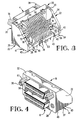
- the housing 2 is best seen in Figures 3 and 6.
- the housing 2 has a pair of board engaging members in the form of opposed, rudimentary, bottom walls 30 projecting inwardly of the housing 2, from the side walls 22, proximate to their bottom edges 26.
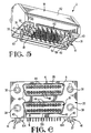
- Each wall 30 has a board engaging bottom face 31 ( Figures 5, 10 and 11).
- the housing 2 also has a rudimentary forward top wall 32 extending rearwardly from the upper end of the front wall 20 and spanning the side walls 22.
- Each edge 24 is joined to the top wall 32 at a short, horizontal top edge 33.
- the front wall 20 is formed with a pair of spaced keys 36 cast therein or threadably securable thereto with key 36 being representative of both versions, near its upper end, each key 36 being located proximate to a respective side wall 22. Below each key 36 the front wall 20 is formed with threaded screw-locks 38. The keys 36 and the screw-locks 38 are provided for cooperation with complimentary key-ways and jack screws, respectively, of an electrical connector (not shown) for mating with the connector 1.
- Keys 36 may have a threaded shank receivable in a threaded aperture in front wall 20 or may be cast into housing 2. Keys 36 project forwardly of wall 20 and have a keying rib 87 thereon. Typically the keys are provided in pairs with the rib 87 on each key 36 oriented in the coordinated directions. The rib 87 may take on other angular positions. Typical positions are at equal angular orientations such as vertically as shown, both laterally outwardly - the rib on the left key to the left and the rib on the right key to the right -, and both vertically downward. The central bore of the key may be threaded to receive a jackscrew. The same structure as key 36, without rib 87, forms a screwlock.
- the front wall 20 is formed with an upper, laterally elongate, through opening 35, and between the keyways 38, with a lower, lateral, elongate through opening 133, as shown in Figure 6.
- Each bottom wall 30 is formed with an inwardly projecting lower step 40 extending the full length thereof and has a central through bore 39 extending through the board engaging face 31 of the wall 30, in which is secured a hollow board lock 41, in the manner described in, and being constructed according to, the teaching of U.S. Patent No. 4,842,552.
- Each board lock 41 comprises an annular strap supported in the respective bore 39 and from which strap depend below the face 31 four locking legs 37.
- each board lock 41 there depends from each bottom wall 30 of the housing 2, on each side of each board lock 41 therein, a board mounting protrusion 43.
- the inner face of each side wall 22 is formed, just above the respective bottom wall 30, with a longitudinal latching groove 42 extending the full length of the side wall 22.
- the drawn shells 4 and 6, which are constructed according to the teaching of U.S. Patent No. 4,808,125 are secured in the openings 35 and 133 respectively, according to the teaching of that U.S. Patent. In this manner, both shells 4 and 6 are electrically commoned with housing 2.
- a shielded mating connector engaging either shell 4 or 6 is grounded to a circuit board on which connector 1 is mounted through housing 2 and boardlock 41 to a ground trace on the circuit board.
- the headers 8 and 10 are secured in the shells 4 and 6, respectively, also in the manner taught by U.S. Patent No. 4,808,125.
- Each header 8 and 10 has an upper row of terminal receiving, through cavities 44. Each cavity 44 and 46 opens into a front mating face 48, and a rear terminal receiving face 50, of the respective header 8 and 10.
- the plate 16 rests upon the steps 40 of the bottom walls 30 and has lugs 52 and 54 at each end of the plate 16, which engage in complimentary recesses of the inner faces 56 of the walls 30.
- the plate 16 has a rear 63, extending the full length thereof.
- the group 12 of terminals comprises an upper row of first terminals 64 and a lower row of second terminals 66, the group 14 of terminals comprising an upper row of third terminals 68 and a lower row of fourth terminals 70.
- Each terminal 64, 66, 68, 70 is uniplanar and comprises a forked, forward mating portion 72, a retention portion 74 extending rearwardly therefrom, the portions 72 and 74 being rectilinear and being longitudinally aligned with each other, a rectilinear leg 76 extending rearwardly from the portion 74 and being downwardly angled with respect thereto, and terminating in a solder tail 78 depending from the bottom of the leg 76 at right angles to the portions 72 and 74.
- the mating portions 72 of the terminals 64 are received in respective cavities 44 of the upper row of cavities of the header 8, the mating portions 72 of the terminals 66, being received the cavities 46 of the lower row of cavities 46 of the header 8.
- the mating portions 72 of the terminals 68 are received in respective cavities 44 of the upper row of cavities of the header 10, the mating portions 72 of the terminals 70 being received in the cavities 46 of the lower row of cavities of the header 10.
- the retention portions 74 of the terminals each of which portions is transversely enlarged, in its own plane, serve to retain the terminals in the cavities, with the forked mating portions 72 of the terminals projecting towards the respective mating faces 48.
- the legs 76 of the terminals 64 are longer than those of the terminals 66, the legs 76 of the terminals 66 being longer than those of the terminals 68 and the legs 76 of the terminals 68 being longer than the legs 76 of the terminals 70.
- the downward angle of the legs 76 of the terminals 64 may be less than that of the legs 76 of the terminals 76, the angle of the legs 76 of the terminals 66 being less than that of the terminals 68 and the angle of the legs 76 of the terminals 68 being less than that of the legs of the terminals 70.
- the solder tails 78 of the terminals 64 extend through the holes of the rearmost row of holes 62 in the plate 16, the tails 78 of the terminals 66 extending through the holes of the next rearmost row of holes 62, the tails 78 of the terminals 68 extending through the holes of next row of holes 62 in the forward direction and the tails 78 of the terminals 70 extending through the holes of the foremost row of holes 62 in the plate 16.
- the spacer plate 16 is pressed over the tails 78.
- shield 18 which has been stamped and formed from a single piece of sheet metal stock, comprises opposite side walls 80 of substantially triangular shape, a rear wall generally referenced 82 and a top wall in the form of a forwardly projecting cantilever flap 84 which is free of the walls 80, the shield 18 being open forwardly.
- the rear wall 82 comprises a rearwardly, and downwardly, inclined upper forward portion 86, a lower rear portion 88, and a lowermost rear portion 90 depending below the side walls 80 and having a bottom edge 91.
- the side walls 80 are connected only by the wall portions 86 and 88.
- the side walls 80 have vertical forward edges 92, surmounted by forwardly and downwardly inclined edge portions 94 configured to allow resilient flexure of the flap 84 as will best be apparent from Figure 9.
- Each sidewall 80 may have a lateral positioning window 97 (shown in Figures 9, 13 and 14) to prevent lateral movement of shield 18 in housing 2 prior to soldering.
- the window engages the inner surface of sidewalls 22 to prevent the lateral motion, and concomitantly provide additional points of electrical continuity therebetween.
- the side walls 80 have bottom edges 96. Each side wall 80 has, proximate to its bottom edge 96, a pair of struck out, outwardly and upwardly inclined, latching tongues 98. Between its tongues 98, each side wall 80 has a central, flat, grounding tab 100, connected to the edge 96 of the wall 80 by a horizontal strap 102 normally thereof. Each tab 100 is thereby offset inwardly of the respective wall 80 in parallel relationship therewith. There may depend from the bottom edge 91 of the wall portion 88 a pair of further flat grounding tabs 104, which are coplanar therewith and the planes of which extend at right angles with those of the tabs 100. The free ends of the tabs 104 may lie below those of the tabs 100.
- the shield 18 In order to mount the shield 18 to the partially completed connector shown in Figure 3, the shield 18 is moved down vertically with its tabs 100 and 104 leading, into the die-cast metal housing 2, so that the latching tongues 98 on each side wall 80 of the shield 18 are initially pressed inwardly and then resile outwardly to latch into respective grooves 42 in the side walls 22 of the housing 2. Windows 97, if present, are pressed inwardly but biasingly engage the inner surface of walls 22.
- the flap 84 of the shield 18 is simultaneously resiliently depressed and inserted under the top wall 32 of the housing 2.
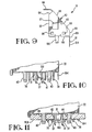
- each tab 100 thereof projects through the annular strap of a respective one of the board locks 41, and extends between the locking legs 37 thereof, as best seen in Figure 10.
- the resilient engagement of the flap 84 against the top wall 32 urges the bottom edge 96 of the shield 18 down against the bottom walls 30.
- the complete connector 1 is shown in Figures 2, and 4 to 6.
- the circuit board PCB ( Figure 2) upon which the assembly 1 is to be surface mounted, has provided therein an array of smaller, plated through holes H1 for receiving the terminal tails 78, two larger, plated through holes H2 for receiving the board locks 41, two further, plated through holes H3 for receiving the tabs 104, four further through, unplated holes H4 for receiving the mounting protrusions 43 of the housing 2.
- shield 18 When shield 18 has as many tabs 100 (or 104) as the connector has boardlocks, there are no additional through holes required solely to accommodate additional shield grounding tabs. When shield 18 has more tabs 100 (or 104) than boardlocks, the number of through holes required can be minimized by having at least some of the through holes perform a dual function of providing a boardlocking function, and possibly concomitantly grounding through the boardlock, as well as providing a path to ground for a ground tab on shield 18.
- the board locks 41 serve to protect the tabs 100 from stubbing against the board PCB when the connector 1 is being mounted thereto, or being otherwise damaged when the connector 1 is being handled.
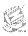
- the connector 1' shown in Figure 12 is the same as connector 1 described above, excepting that the tabs 104 of the shield are not provided. The provision of the holes H3 in the circuit board is accordingly avoided.
- a shield 18' is the same as the shield 18, excepting that the wall portion 86' of the rear wall 82' is formed with rows of holes 108 provided with struck out, semi-circular funnels 110 extending thereabout for the introduction of cleaning fluids, which may be liquids or gases, to flush out debris from beneath the terminal tail spacer plate.
- cleaning fluids which may be liquids or gases
- the liquids may flush out debris that might otherwise short between solder tails; air may be used to dry. This may be achieved with shield 18' in place.
- the wall portion 88' is provided with a rearwardly inclined flap 112 to allow for the egress of the said fluids.
Landscapes
- Details Of Connecting Devices For Male And Female Coupling (AREA)
- Coupling Device And Connection With Printed Circuit (AREA)
Description
- The present invention relates to an electrical connector for mounting to a circuit board having a metal shield.
- U.S. Patent No. 5,037,330 discloses a right angle electrical connector having a metal shield having side walls from which project struck out flanges which engage in external grooves in insulating housings of the connector which are received within the shield and with bowed mounting feet projecting from bottom edges of the shield side walls for insertion through holes in a circuit board to retain the connector thereon.
- The electrical connector of the above construction has the following advantages. The metal shield covers the entirety of the upper and lower electrical connector bodies while providing a pair of mounting legs for ready assembly. Additionally, the shield has detent members which provide a stable structural connection to the electrical connectors.
- However, on the other hand, the electrical connector having the above construction has the following disadvantages. The connector lacks board mounts on the bottom electrical connector and is therefore not firmly retained in place until the metal shield covers it. Further, the metal shield's mounting legs do not firmly fix the electrical connector to the printed circuit board because they have only one leg each. Additionally, the single leg design has the chance of being bent or otherwise damaged.
- The instant invention overcomes the above-mentioned problems. The object of the present invention is to provide a multi-leg board lock which firmly fixes the connector assembly to a printed circuit board. Further, the shield's legs are soldered to the board lock in a way that eliminates the need for another hole in the printed circuit board.
- The present invention consists in an electrical connector as defined in claim 1.
- An electrical connector according to the preamble of claim 1 is disclosed in EP-A-0 292 144.
- As disclosed herein, an electrical connector is provided for mounting on a circuit board and includes a housing having a bottom wall with a bottom face for engaging against the circuit board, the bottom wall having formed therein a through bore opening into said bottom face. A hollow board lock supported in the through bore, has locking legs projecting below the bottom face for insertion in a first hole in the circuit board. A header in the housing carries electrical terminals with terminal legs thereof projecting from the header and terminating in soldering tails depending below the bottom face of the housing for insertion into second holes in the circuit board with the bottom face of the housing engaging it. A metal shield covering the terminal legs has depending therefrom a grounding tab projecting through the board lock and between the locking legs thereof.
- When the connector has been mounted on the circuit board, with the locking legs of the board lock projecting through the first hole and the soldering tails projecting through the second holes, the board lock and the soldering tails are soldered to respective ground and signal conductors on the underside of the board. The grounding tab which projects between the locking legs of the board lock, is soldered to the same grounding conductor. The drilling program for the board is thereby simplified and lining metal is saved. Further, the board lock serves to protect the grounding tab from stubbing against the board when the connector is being mounted thereto, or the grounding tab being otherwise damaged when the connector is being handled.
- The bores for the board locks may be formed in spaced, rudimentary bottom walls of the housing, the housing having a top wall and the shield having a top flap resiliently engaging beneath the top wall of the housing whereby the side walls of the shield, from which the grounding tabs project, are resilient urged against said bottom walls of the housing. The shield may be received between side walls projecting from a front wall of the housing in which the header is fixed, a side wall of the shield having latching tongues engaged in grooves in the housing side walls. In order to assemble the shield to the housing, the shield is moved down vertically between the side walls, so that the grounding tabs enter the board locks and the latching tongues engage the grooves, the flap being resiliently depressed and located beneath the top wall of the housing. In order to locate the grounding tabs for insertion through the board locks, the grounding tabs are offset inwardly from the side walls of the shield.
- As disclosed herein, a right angle electrical connector for mounting on a circuit board comprises a die-cast metal housing having a front wall formed with upper and lower through openings. Side walls project from opposite lateral ends of the front wall rearwardly thereof, board engaging bottom walls extending towards each other from inner faces of the side walls. Projections depend from the bottom walls for electrically connecting the diecast metal housing to ground by way of the circuit board. A first drawn metal shell defining a through aperture is secured in the upper through opening of the metal housing and a second drawn metal shell is secured in the lower through opening of the metal housing. A first insulating header is received in the aperture of the first drawn shell and a second insulating header is received in the aperture of the second drawn shell. Each header has a mating face exposed in the forward direction of the housing front wall and a terminal receiving face directed rearwardly of the housing front wall. The first header comprises a first group of electrical terminals, the second header comprising a second group of electrical terminals. Each terminal has a mating portion within the header which is exposed towards the mating face of the header, a terminal leg projecting obliquely downwardly and rearwardly beyond the terminal receiving face of the header and between the housing side walls and a soldering tail projecting downwardly below the bottom walls of the housing. The solder tails of the terminals of each group of terminals are arranged in at least one row, all of said rows being parallel.
- An embodiment of the present invention will now be described by way of example with reference to the accompanying drawings in which:
- FIGURE 1 is an exploded isometric view of a stacked, right angle electrical connector showing a preferred embodiment of a metal shield thereof;
- FIGURE 2 is a rear isometric view of the connector in its assembled state, exploded from a circuit board;
- FIGURE 3 is a rear isometric view of the connector of Figure 2, with the shield removed;
- FIGURE 4 is a front isometric view of the connector of Figure 2;
- FIGURE 5 is a bottom isometric view of the connector of Figure 2;
- FIGURE 6 is a front elevational view of the connector of Figure 2;
- FIGURE 7 is an isometric view of the metal shield of the connector of Figure 2;
- FIGURE 8 is a front elevational view of the shield of Figure 7 showing the interior thereof;
- FIGURE 9 is an end view of the shield of Figures 7 and 8;
- FIGURE 10 is a fragmentary side view illustrating details of the connector of Figure 2;
- FIGURE 11 is a fragmentary side view shown partly in section illustrating details of the connector of Figure 2, when it has been mounted to the circuit board;
- FIGURE 12 is a similar view to that of Figure 2, but illustrating a modification of the metal shield;
- FIGURE 13 is a rear isometric view illustrating further modifications of the metal shield; and
- FIGURE 14 is an end view of the shield of Figure 13.
- A shielded, stacked, right angle, electrical connector 1, for mounting on a circuit board PCB, is shown in the exploded perspective view of Figure 1. The connector, which may be used in the computer field as an input/output port, comprises a die
cast metal housing 2, receiving upper and lower drawnmetal shells shells lower header inserts inserts lower groups tail spacer plate 16 and ametal shield 18 covering the rear of thehousing 2. The connector 1 will now be described with reference to Figures 1 to 11. - The
die cast housing 2 comprises afront wall 20 andopposite side walls 22 tapering rearwardly from opposite ends of thefront wall 20, eachside wall 22 having a downwardly inclinedupper edge 24, ahorizontal bottom edge 26 extending at right angles to thefront wall 20 and a verticalrear edge 28 joining theedges wall 20. Thehousing 2 is best seen in Figures 3 and 6. Thehousing 2 has a pair of board engaging members in the form of opposed, rudimentary,bottom walls 30 projecting inwardly of thehousing 2, from theside walls 22, proximate to theirbottom edges 26. Eachwall 30 has a board engaging bottom face 31 (Figures 5, 10 and 11). Thehousing 2 also has a rudimentaryforward top wall 32 extending rearwardly from the upper end of thefront wall 20 and spanning theside walls 22. Eachedge 24 is joined to thetop wall 32 at a short, horizontaltop edge 33. - The
front wall 20 is formed with a pair ofspaced keys 36 cast therein or threadably securable thereto with key 36 being representative of both versions, near its upper end, eachkey 36 being located proximate to arespective side wall 22. Below eachkey 36 thefront wall 20 is formed with threaded screw-locks 38. Thekeys 36 and the screw-locks 38 are provided for cooperation with complimentary key-ways and jack screws, respectively, of an electrical connector (not shown) for mating with the connector 1. -
Keys 36 may have a threaded shank receivable in a threaded aperture infront wall 20 or may be cast intohousing 2. Keys 36 project forwardly ofwall 20 and have akeying rib 87 thereon. Typically the keys are provided in pairs with therib 87 on each key 36 oriented in the coordinated directions. Therib 87 may take on other angular positions. Typical positions are at equal angular orientations such as vertically as shown, both laterally outwardly - the rib on the left key to the left and the rib on the right key to the right -, and both vertically downward. The central bore of the key may be threaded to receive a jackscrew. The same structure as key 36, withoutrib 87, forms a screwlock. - As shown in Figure 6 between the
keys 36, thefront wall 20 is formed with an upper, laterally elongate, throughopening 35, and between thekeyways 38, with a lower, lateral, elongate throughopening 133, as shown in Figure 6. Eachbottom wall 30 is formed with an inwardly projectinglower step 40 extending the full length thereof and has a central throughbore 39 extending through theboard engaging face 31 of thewall 30, in which is secured ahollow board lock 41, in the manner described in, and being constructed according to, the teaching of U.S. Patent No. 4,842,552. Eachboard lock 41 comprises an annular strap supported in therespective bore 39 and from which strap depend below theface 31 four lockinglegs 37. There depends from eachbottom wall 30 of thehousing 2, on each side of eachboard lock 41 therein, aboard mounting protrusion 43. The inner face of eachside wall 22 is formed, just above therespective bottom wall 30, with alongitudinal latching groove 42 extending the full length of theside wall 22. - The drawn
shells openings shells housing 2. A shielded mating connector engaging eithershell housing 2 andboardlock 41 to a ground trace on the circuit board. Theheaders shells header cavities 44. Eachcavity front mating face 48, and a rearterminal receiving face 50, of therespective header - The
plate 16 rests upon thesteps 40 of thebottom walls 30 and haslugs plate 16, which engage in complimentary recesses of the inner faces 56 of thewalls 30. Theplate 16 has a rear 63, extending the full length thereof. There are provided in theplate 16, a plurality of longitudinally extending rows of terminal tail receiving throughholes 62. - The
group 12 of terminals comprises an upper row offirst terminals 64 and a lower row ofsecond terminals 66, thegroup 14 of terminals comprising an upper row ofthird terminals 68 and a lower row offourth terminals 70. Each terminal 64, 66, 68, 70 is uniplanar and comprises a forked,forward mating portion 72, aretention portion 74 extending rearwardly therefrom, theportions rectilinear leg 76 extending rearwardly from theportion 74 and being downwardly angled with respect thereto, and terminating in asolder tail 78 depending from the bottom of theleg 76 at right angles to theportions mating portions 72 of theterminals 64 are received inrespective cavities 44 of the upper row of cavities of theheader 8, themating portions 72 of theterminals 66, being received thecavities 46 of the lower row ofcavities 46 of theheader 8. Themating portions 72 of theterminals 68 are received inrespective cavities 44 of the upper row of cavities of theheader 10, themating portions 72 of theterminals 70 being received in thecavities 46 of the lower row of cavities of theheader 10. Theretention portions 74 of the terminals, each of which portions is transversely enlarged, in its own plane, serve to retain the terminals in the cavities, with the forkedmating portions 72 of the terminals projecting towards the respective mating faces 48. Thelegs 76 of theterminals 64 are longer than those of theterminals 66, thelegs 76 of theterminals 66 being longer than those of theterminals 68 and thelegs 76 of theterminals 68 being longer than thelegs 76 of theterminals 70. The downward angle of thelegs 76 of theterminals 64 may be less than that of thelegs 76 of theterminals 76, the angle of thelegs 76 of theterminals 66 being less than that of theterminals 68 and the angle of thelegs 76 of theterminals 68 being less than that of the legs of theterminals 70. - By virtue of these configurations of the
legs 76, thesolder tails 78 of theterminals 64 extend through the holes of the rearmost row ofholes 62 in theplate 16, thetails 78 of theterminals 66 extending through the holes of the next rearmost row ofholes 62, thetails 78 of theterminals 68 extending through the holes of next row ofholes 62 in the forward direction and thetails 78 of theterminals 70 extending through the holes of the foremost row ofholes 62 in theplate 16. Thespacer plate 16 is pressed over thetails 78. - As best seen in Figures 7 to 9,
shield 18, which has been stamped and formed from a single piece of sheet metal stock, comprisesopposite side walls 80 of substantially triangular shape, a rear wall generally referenced 82 and a top wall in the form of a forwardly projectingcantilever flap 84 which is free of thewalls 80, theshield 18 being open forwardly. Therear wall 82 comprises a rearwardly, and downwardly, inclined upperforward portion 86, a lowerrear portion 88, and a lowermostrear portion 90 depending below theside walls 80 and having abottom edge 91. Theside walls 80 are connected only by thewall portions side walls 80 have vertical forward edges 92, surmounted by forwardly and downwardlyinclined edge portions 94 configured to allow resilient flexure of theflap 84 as will best be apparent from Figure 9. Eachsidewall 80 may have a lateral positioning window 97 (shown in Figures 9, 13 and 14) to prevent lateral movement ofshield 18 inhousing 2 prior to soldering. The window engages the inner surface ofsidewalls 22 to prevent the lateral motion, and concomitantly provide additional points of electrical continuity therebetween. - The
side walls 80 havebottom edges 96. Eachside wall 80 has, proximate to itsbottom edge 96, a pair of struck out, outwardly and upwardly inclined, latchingtongues 98. Between itstongues 98, eachside wall 80 has a central, flat,grounding tab 100, connected to theedge 96 of thewall 80 by ahorizontal strap 102 normally thereof. Eachtab 100 is thereby offset inwardly of therespective wall 80 in parallel relationship therewith. There may depend from thebottom edge 91 of the wall portion 88 a pair of furtherflat grounding tabs 104, which are coplanar therewith and the planes of which extend at right angles with those of thetabs 100. The free ends of thetabs 104 may lie below those of thetabs 100. - In order to mount the
shield 18 to the partially completed connector shown in Figure 3, theshield 18 is moved down vertically with itstabs cast metal housing 2, so that the latchingtongues 98 on eachside wall 80 of theshield 18 are initially pressed inwardly and then resile outwardly to latch intorespective grooves 42 in theside walls 22 of thehousing 2.Windows 97, if present, are pressed inwardly but biasingly engage the inner surface ofwalls 22. Theflap 84 of theshield 18 is simultaneously resiliently depressed and inserted under thetop wall 32 of thehousing 2. In this manner, therear wall portions shield 18 cover the rear edges of the terminals of thegroups rear wall portion 90 of theshield 18 abutting in face-to-face relationship against therear wall 63 of thespacer plate 16 and thetabs 104 projecting therebelow and therebehind. In this assembled position of theshield 18, eachtab 100 thereof projects through the annular strap of a respective one of the board locks 41, and extends between the lockinglegs 37 thereof, as best seen in Figure 10. The resilient engagement of theflap 84 against thetop wall 32 urges thebottom edge 96 of theshield 18 down against thebottom walls 30. The complete connector 1 is shown in Figures 2, and 4 to 6. - The circuit board PCB (Figure 2) upon which the assembly 1 is to be surface mounted, has provided therein an array of smaller, plated through holes H1 for receiving the
terminal tails 78, two larger, plated through holes H2 for receiving the board locks 41, two further, plated through holes H3 for receiving thetabs 104, four further through, unplated holes H4 for receiving the mountingprotrusions 43 of thehousing 2. - When the connector 1 has been mounted to the board PCB with the
terminal tails 78, the board locks 41, thetabs 104 and the mountingprotrusions 43 projecting through the holes provided for them in the board PCB, as shown in Figure 11, the parts projecting below the board PCB, of theterminal tails 78, are soldered to respective signal conductors (not shown) on the board PCB, the lockinglegs 37 of the board locks 41, and thetabs 104 being soldered to ground conductors (not shown) on the board PCB. Since thetabs 100 extend into the board locks 41, they are likewise soldered to the grounding conductors to which thelegs 37 are soldered, as shown in Figure 11. No additional plated through holes in the board PCB have, therefore, to be provided for thetabs 100. The drilling program for the board is thereby simplified and lining metal is saved. - When
shield 18 has as many tabs 100 (or 104) as the connector has boardlocks, there are no additional through holes required solely to accommodate additional shield grounding tabs. Whenshield 18 has more tabs 100 (or 104) than boardlocks, the number of through holes required can be minimized by having at least some of the through holes perform a dual function of providing a boardlocking function, and possibly concomitantly grounding through the boardlock, as well as providing a path to ground for a ground tab onshield 18. - Further, the board locks 41 serve to protect the
tabs 100 from stubbing against the board PCB when the connector 1 is being mounted thereto, or being otherwise damaged when the connector 1 is being handled. - The connector 1' shown in Figure 12 is the same as connector 1 described above, excepting that the
tabs 104 of the shield are not provided. The provision of the holes H3 in the circuit board is accordingly avoided. - As shown in Figures 13 and 14, a shield 18' according to an alternative embodiment, is the same as the
shield 18, excepting that the wall portion 86' of the rear wall 82' is formed with rows ofholes 108 provided with struck out,semi-circular funnels 110 extending thereabout for the introduction of cleaning fluids, which may be liquids or gases, to flush out debris from beneath the terminal tail spacer plate. The liquids may flush out debris that might otherwise short between solder tails; air may be used to dry. This may be achieved with shield 18' in place. The wall portion 88' is provided with a rearwardlyinclined flap 112 to allow for the egress of the said fluids.
Claims (8)
- An electrical connector (1) for mounting to a printed circuit board (PCB), the connector (1) having at least one header insert (8) disposed within a die-cast metal housing (2) an within a metal shield (18) for incorporating at least one group of electrical terminals (12), characterized in that; the metal housing (2) includes an aperture (39) with a hollow board lock (41) disposed therein, the board lock including at least two legs (37) and the metal shield (18) including tabs (100) which are received within the hollow portion of the board lock (41) for soldering therewith.
- An electrical connector as claimed in claim 1, characterised in that the metal housing (2) includes a removable tail spacer plate (16) for supporting the terminals (12).
- An electrical connector as claimed in claim 2, characterised in that the at least one header insert (8) is disposed in a drawn metal shell (4).
- An electrical connector as claimed in claim 2, characterised in that the terminals (12) are planar.
- An electrical connector as claimed in any one of the preceding claims, characterised in that the at least two legs (37) are bent along their length so that they cantilever inwardly when placed in the aperture (39).
- An electrical connector as claimed in any one of claims 1 to 4, characterised in that the metal shield (18) includes grounding tabs (104) and a cantilever flap (84) which cooperate together to secure the metal shield (18) to the metal housing (2) and printed circuit board (PCB).
- An electrical connector as claimed in claim 6, characterised in that the metal shield (18) has latching tongues (98) which engage grooves (42) in the metal housing (2).
- An electrical connector as claimed in claim 6, characterised in that the metal shield (18) includes funnels (110) for the ingress of a cleaning fluid.
Applications Claiming Priority (4)
| Application Number | Priority Date | Filing Date | Title |
|---|---|---|---|
| US853565 | 1992-03-18 | ||
| US07/853,565 US5167531A (en) | 1992-03-18 | 1992-03-18 | Stacked electrical connector with diecast housing and drawn shells |
| US07/853,649 US5161999A (en) | 1992-03-18 | 1992-03-18 | Surface mount electrical cohnnector and shield therefor |
| US853649 | 1992-03-18 |
Publications (2)
| Publication Number | Publication Date |
|---|---|
| EP0561497A1 EP0561497A1 (en) | 1993-09-22 |
| EP0561497B1 true EP0561497B1 (en) | 1997-04-16 |
Family
ID=27127170
Family Applications (1)
| Application Number | Title | Priority Date | Filing Date |
|---|---|---|---|
| EP93300980A Expired - Lifetime EP0561497B1 (en) | 1992-03-18 | 1993-02-11 | Surface mount electrical connector and shield therefor |
Country Status (4)
| Country | Link |
|---|---|
| EP (1) | EP0561497B1 (en) |
| JP (1) | JP2892903B2 (en) |
| KR (1) | KR0183463B1 (en) |
| DE (1) | DE69309761T2 (en) |
Cited By (1)
| Publication number | Priority date | Publication date | Assignee | Title |
|---|---|---|---|---|
| US6106332A (en) * | 1996-10-15 | 2000-08-22 | The Whitaker Corporation | Board lock for electrical connector |
Families Citing this family (23)
| Publication number | Priority date | Publication date | Assignee | Title |
|---|---|---|---|---|
| SE502998C2 (en) * | 1994-06-10 | 1996-03-11 | Ericsson Telefon Ab L M | Electrical connector and circuit board |
| JP2942985B2 (en) * | 1995-11-16 | 1999-08-30 | モレックス インコーポレーテッド | Electrical connector |
| JPH11135187A (en) * | 1997-10-30 | 1999-05-21 | Fujitsu Takamisawa Component Ltd | Connector consolidated package |
| US6287146B1 (en) * | 1999-02-04 | 2001-09-11 | Molex Incorporated | Grounded electrical connector with tail aligner |
| NL1012365C2 (en) * | 1999-06-16 | 2000-12-19 | Berg Electronics Mfg | Connector has contact elements mounted in housing, in which grooves extend transversely |
| WO2000077887A1 (en) * | 1999-06-16 | 2000-12-21 | Fci 's-Hertogenbosch B.V. | Connector, method for manufacturing such a connector and contact element for a connector |
| MY121506A (en) * | 2000-02-10 | 2006-01-28 | Molex Inc | Electric combination connector set |
| US6494724B1 (en) * | 2001-10-02 | 2002-12-17 | Molex Incorporated | Electrical connector with terminal tail aligning device |
| US7168987B1 (en) * | 2005-07-12 | 2007-01-30 | Fujitsu Component Limited | Right angle type connector used for balanced transmission of data signals |
| JP4861055B2 (en) * | 2006-05-24 | 2012-01-25 | 矢崎総業株式会社 | connector |
| WO2009083757A1 (en) * | 2007-12-28 | 2009-07-09 | Fci | Electrical connector and shroud therefor |
| WO2015183951A1 (en) * | 2014-05-30 | 2015-12-03 | Molex Incorporated | Electrical connector with terminal holder |
| DE102017127482A1 (en) * | 2017-11-21 | 2019-05-23 | Phoenix Contact Gmbh & Co. Kg | Connectors |
| JP7222178B2 (en) * | 2018-03-23 | 2023-02-15 | I-Pex株式会社 | Dust cover and connector |
| US10797417B2 (en) | 2018-09-13 | 2020-10-06 | Amphenol Corporation | High performance stacked connector |
| CN208862209U (en) | 2018-09-26 | 2019-05-14 | 安费诺东亚电子科技(深圳)有限公司 | A kind of connector and its pcb board of application |
| WO2020154526A1 (en) | 2019-01-25 | 2020-07-30 | Fci Usa Llc | I/o connector configured for cabled connection to the midboard |
| CN116247455A (en) | 2019-01-25 | 2023-06-09 | 富加宜(美国)有限责任公司 | electrical connector |
| US11444404B2 (en) | 2019-09-27 | 2022-09-13 | Fci Usa Llc | High performance stacked connector |
| CN113258325A (en) | 2020-01-28 | 2021-08-13 | 富加宜(美国)有限责任公司 | High-frequency middle plate connector |
| US12212100B2 (en) | 2021-04-30 | 2025-01-28 | Amphenol Corporation | Miniaturized high speed connector |
| DE102021134344A1 (en) | 2021-12-22 | 2023-06-22 | HARTING Electronics GmbH | Printed circuit board connectors with a form element that can be sensed |
| CN119231218B (en) * | 2024-09-03 | 2025-11-14 | 上海航天科工电器研究院有限公司 | High-speed connectors with coplanar mounting |
Family Cites Families (6)
| Publication number | Priority date | Publication date | Assignee | Title |
|---|---|---|---|---|
| US4822303A (en) * | 1987-05-18 | 1989-04-18 | Hirose Electric Co., Ltd. | Electrical connector |
| JPH02150682U (en) * | 1989-05-22 | 1990-12-27 | ||
| US4902242A (en) | 1989-05-31 | 1990-02-20 | Amp Incorporated | Panel mount, cable terminable connector with die cast housing and drawn shell |
| DE59007211D1 (en) * | 1989-08-10 | 1994-10-27 | Siemens Ag | Device for the electrical connection of shields of multipole plugs to the ground potential layer of a wiring board. |
| US5037331A (en) * | 1989-09-27 | 1991-08-06 | Itt Corporation | Shielded interface connector |
| US5161999A (en) * | 1992-03-18 | 1992-11-10 | Amp Incorporated | Surface mount electrical cohnnector and shield therefor |
-
1993
- 1993-02-11 EP EP93300980A patent/EP0561497B1/en not_active Expired - Lifetime
- 1993-02-11 DE DE69309761T patent/DE69309761T2/en not_active Expired - Fee Related
- 1993-03-08 KR KR1019930003406A patent/KR0183463B1/en not_active Expired - Fee Related
- 1993-03-18 JP JP5085620A patent/JP2892903B2/en not_active Expired - Fee Related
Cited By (1)
| Publication number | Priority date | Publication date | Assignee | Title |
|---|---|---|---|---|
| US6106332A (en) * | 1996-10-15 | 2000-08-22 | The Whitaker Corporation | Board lock for electrical connector |
Also Published As
| Publication number | Publication date |
|---|---|
| KR0183463B1 (en) | 1999-05-15 |
| DE69309761D1 (en) | 1997-05-22 |
| KR930020771A (en) | 1993-10-20 |
| JP2892903B2 (en) | 1999-05-17 |
| EP0561497A1 (en) | 1993-09-22 |
| JPH0629061A (en) | 1994-02-04 |
| DE69309761T2 (en) | 1997-11-13 |
Similar Documents
| Publication | Publication Date | Title |
|---|---|---|
| US5167531A (en) | Stacked electrical connector with diecast housing and drawn shells | |
| US5161999A (en) | Surface mount electrical cohnnector and shield therefor | |
| EP0561497A1 (en) | Surface mount electrical connector and shield therefor | |
| US6343951B1 (en) | Electrical connector | |
| US7108554B2 (en) | Electrical connector with shielding member | |
| CN1119844C (en) | Shielded electrical connector | |
| US6210218B1 (en) | Electrical connector | |
| US6227879B1 (en) | Electrical connector with grounding shroud having board-locks for grasping a circuit board | |
| US5044984A (en) | Stackable connector assembly and bracket therefor | |
| US6814612B1 (en) | Shielded electrical connector | |
| EP0624928B1 (en) | Shielded electrical connector assembly | |
| US6183273B1 (en) | Stacked electrical card connector assembly | |
| US5709556A (en) | Connector with auxiliary alignment plate | |
| US4080041A (en) | Electrical connector | |
| US6210226B1 (en) | Electrical connector having enhanced sideward impact resisting structure | |
| US20080020640A1 (en) | Electrical connector with shell | |
| US20080032560A1 (en) | Electrical connector assembly | |
| US6089916A (en) | Cable assembly connector | |
| US6086429A (en) | Low profile connector | |
| US5137472A (en) | Means for securing ground plates to electrical connector housing | |
| US20050287860A1 (en) | Interlocking member for an electrical connector | |
| US6508665B1 (en) | Electrical connector having printed circuit board mounted therein | |
| US6036506A (en) | Right angle electrical connector | |
| US6102734A (en) | Electrical connector | |
| US6458001B1 (en) | Receptacle connector having anti-mismating structures |
Legal Events
| Date | Code | Title | Description |
|---|---|---|---|
| PUAI | Public reference made under article 153(3) epc to a published international application that has entered the european phase |
Free format text: ORIGINAL CODE: 0009012 |
|
| AK | Designated contracting states |
Kind code of ref document: A1 Designated state(s): DE FR GB IT NL |
|
| 17P | Request for examination filed |
Effective date: 19940317 |
|
| 17Q | First examination report despatched |
Effective date: 19950810 |
|
| GRAG | Despatch of communication of intention to grant |
Free format text: ORIGINAL CODE: EPIDOS AGRA |
|
| GRAH | Despatch of communication of intention to grant a patent |
Free format text: ORIGINAL CODE: EPIDOS IGRA |
|
| GRAH | Despatch of communication of intention to grant a patent |
Free format text: ORIGINAL CODE: EPIDOS IGRA |
|
| GRAA | (expected) grant |
Free format text: ORIGINAL CODE: 0009210 |
|
| AK | Designated contracting states |
Kind code of ref document: B1 Designated state(s): DE FR GB IT NL |
|
| ITF | It: translation for a ep patent filed | ||
| REF | Corresponds to: |
Ref document number: 69309761 Country of ref document: DE Date of ref document: 19970522 |
|
| ET | Fr: translation filed | ||
| PLBE | No opposition filed within time limit |
Free format text: ORIGINAL CODE: 0009261 |
|
| STAA | Information on the status of an ep patent application or granted ep patent |
Free format text: STATUS: NO OPPOSITION FILED WITHIN TIME LIMIT |
|
| 26N | No opposition filed | ||
| PGFP | Annual fee paid to national office [announced via postgrant information from national office to epo] |
Ref country code: NL Payment date: 19981222 Year of fee payment: 7 |
|
| PGFP | Annual fee paid to national office [announced via postgrant information from national office to epo] |
Ref country code: DE Payment date: 19991229 Year of fee payment: 8 |
|
| PGFP | Annual fee paid to national office [announced via postgrant information from national office to epo] |
Ref country code: FR Payment date: 20000207 Year of fee payment: 8 |
|
| PG25 | Lapsed in a contracting state [announced via postgrant information from national office to epo] |
Ref country code: NL Free format text: LAPSE BECAUSE OF NON-PAYMENT OF DUE FEES Effective date: 20000901 |
|
| NLV4 | Nl: lapsed or anulled due to non-payment of the annual fee |
Effective date: 20000901 |
|
| PG25 | Lapsed in a contracting state [announced via postgrant information from national office to epo] |
Ref country code: FR Free format text: LAPSE BECAUSE OF NON-PAYMENT OF DUE FEES Effective date: 20011031 |
|
| REG | Reference to a national code |
Ref country code: FR Ref legal event code: ST |
|
| PG25 | Lapsed in a contracting state [announced via postgrant information from national office to epo] |
Ref country code: DE Free format text: LAPSE BECAUSE OF NON-PAYMENT OF DUE FEES Effective date: 20011201 |
|
| REG | Reference to a national code |
Ref country code: GB Ref legal event code: IF02 |
|
| PG25 | Lapsed in a contracting state [announced via postgrant information from national office to epo] |
Ref country code: IT Free format text: LAPSE BECAUSE OF NON-PAYMENT OF DUE FEES;WARNING: LAPSES OF ITALIAN PATENTS WITH EFFECTIVE DATE BEFORE 2007 MAY HAVE OCCURRED AT ANY TIME BEFORE 2007. THE CORRECT EFFECTIVE DATE MAY BE DIFFERENT FROM THE ONE RECORDED. Effective date: 20050211 |
|
| PGFP | Annual fee paid to national office [announced via postgrant information from national office to epo] |
Ref country code: GB Payment date: 20060223 Year of fee payment: 14 |
|
| GBPC | Gb: european patent ceased through non-payment of renewal fee |
Effective date: 20070211 |
|
| PG25 | Lapsed in a contracting state [announced via postgrant information from national office to epo] |
Ref country code: GB Free format text: LAPSE BECAUSE OF NON-PAYMENT OF DUE FEES Effective date: 20070211 |