EP0544394B1 - Electrical apparatus - Google Patents
Electrical apparatus Download PDFInfo
- Publication number
- EP0544394B1 EP0544394B1 EP92308550A EP92308550A EP0544394B1 EP 0544394 B1 EP0544394 B1 EP 0544394B1 EP 92308550 A EP92308550 A EP 92308550A EP 92308550 A EP92308550 A EP 92308550A EP 0544394 B1 EP0544394 B1 EP 0544394B1
- Authority
- EP
- European Patent Office
- Prior art keywords
- value
- transfer function
- units
- phase shift
- input signal
- Prior art date
- Legal status (The legal status is an assumption and is not a legal conclusion. Google has not performed a legal analysis and makes no representation as to the accuracy of the status listed.)
- Expired - Lifetime
Links
Images

Classifications
-
- H—ELECTRICITY
- H03—ELECTRONIC CIRCUITRY
- H03H—IMPEDANCE NETWORKS, e.g. RESONANT CIRCUITS; RESONATORS
- H03H17/00—Networks using digital techniques
- H03H17/08—Networks for phase shifting
Definitions
- This invention relates to electrical apparatus.
- the invention relates to electrical apparatus of the kind (hereinafter referred to as the kind specified) comprising a number of units, each of which is capable of presenting to an input signal a transfer function of a different value and control means whereby a desired selection of said units can be made so as to present to the input signal a total value of desired transfer function value within a predetermined range.
- control means typically provides a binary control signal, each digit of which determines whether or not a different one of the controls is selected according to the value of that digit i.e. whether that digit has a value '0' or '1'.
- the control signal is suitably produced by an analogue to digital converter which produces a binary digital output signal in response to an analogue input signal representing the desired total value of said transfer function to a resolution, i.e. number of digits, equal to the number of said units.
- phase shifter which comprises a number of units each of which imposes a different phase shift on the input signal.
- the values of the transfer functions presented by the different units are chosen so that any desired value within the given range of values of the transfer function can be obtained with at least a predetermined accuracy i.e. resolution.
- Such an apparatus is shown in US 4 841 552 which discloses a phase shifter having a number of units each of which presents a phase shift angle of a different value to an input signal. A desired selection of units is made to present to the input signal a desired total phase shift angle. The units present successively smaller phase shift angles, the ratio between each angle and the next smallest angle being 2:1.
- the values of the transfer functions presented by the units are chosen so that the available settable total values of the transfer functions are equally spaced through the desired range.
- the unit presenting the largest value of transfer function presents a transfer function equal to half the desired range
- a second unit presents a transfer function of half this value and so on, the unit presenting the smallest value of transfer function presenting a value equal to or less than the desired resolution.
- the phase shifts of the different units are 180°, 90°, 45°, 22.5° and 11.25°.
- any desired value within the range 0° to 360° can be obtained with a maximum resolution of 11.25° .
- the actual phase shifts presented by the different units are likely also to be subject to error.
- the actual maximum resolution is larger than 11.25°.
- control signal 01111 the highest phase shift unit is selected
- MSB only the unit giving the largest phase shift
- an electrical apparatus comprising control means and a number of units each of which is capable of presenting to an input signal a transfer function of a different value the transfer function values of the units being subject to possible error with respect to their nominal values whereby a desired selection of said units can be made so as to present to the input signal a total value of desired transfer function value within a predetermined range characterised in that the ratio between each nominal transfer function value and the next smallest nominal transfer function value is less than 2:1.
- phase shifter comprising n units, each of which imposes a different phase shift Bi on an input signal, where 0 ⁇ i ⁇ n-1.
- the minimum phase shift value (LSB) is Bo and the maximum phase shift value (MSB) is B n-1 .
- the phase shifter is designed to produce phase shifts within the range R with a predetermined accuracy of at least L.
- the resolution L which can be achieved is determined by the LSB. Where the error in each phase shift value is ⁇ , the value of the LSB varies between Bo(1+ ⁇ ) and Bo 1+ ⁇ where Bo is the nominal value.
- phase shifts Bi (where 0 ⁇ i ⁇ n-1) must not be less than the range R of phase shifts to be produced, even when each phase shift has its minimum value, Bi 1+ ⁇ .
- phase shifter according to the invention will now be described by way of example only.
- the phase shifter includes a control means comprising a circuit 7 and a look-up table 9.
- the circuit 7 receives an analogue signal representative of a desired phase shift to be presented to an input signal by units 1 to 6, each of which present a different phase shift value.
- the circuit 7 is an analogue to digital converter, which passes a five digit binary signal to the look-up table 9.
- the ratio R/L must equal 31.
- a phase shifter capable of presenting the above phase shift values to an input signal can produce a total phase shift of between 0° and 360° to the same resolution as would be achieved with a five unit phase shifter with 0% error, even if the percentage error in each phase shift value is 13%.
Landscapes
- Networks Using Active Elements (AREA)
Description
- This invention relates to electrical apparatus.
- More particularly the invention relates to electrical apparatus of the kind (hereinafter referred to as the kind specified) comprising a number of units, each of which is capable of presenting to an input signal a transfer function of a different value and control means whereby a desired selection of said units can be made so as to present to the input signal a total value of desired transfer function value within a predetermined range.
- In such an apparatus the control means typically provides a binary control signal, each digit of which determines whether or not a different one of the controls is selected according to the value of that digit i.e. whether that digit has a value '0' or '1'.
- The control signal is suitably produced by an analogue to digital converter which produces a binary digital output signal in response to an analogue input signal representing the desired total value of said transfer function to a resolution, i.e. number of digits, equal to the number of said units.
- One example of such an apparatus is a phase shifter which comprises a number of units each of which imposes a different phase shift on the input signal.
- In such an apparatus the values of the transfer functions presented by the different units are chosen so that any desired value within the given range of values of the transfer function can be obtained with at least a predetermined accuracy i.e. resolution.
- Such an apparatus is shown in US 4 841 552 which discloses a phase shifter having a number of units each of which presents a phase shift angle of a different value to an input signal. A desired selection of units is made to present to the input signal a desired total phase shift angle. The units present successively smaller phase shift angles, the ratio between each angle and the next smallest angle being 2:1.
- To this end in a known form of apparatus of the kind specified the values of the transfer functions presented by the units are chosen so that the available settable total values of the transfer functions are equally spaced through the desired range. In such an arrangement the unit presenting the largest value of transfer function presents a transfer function equal to half the desired range, a second unit presents a transfer function of half this value and so on, the unit presenting the smallest value of transfer function presenting a value equal to or less than the desired resolution. For example for a phase shifter settable in the range 0° to 360° using five units and have a five digit binary number as the control signal the phase shifts of the different units are 180°, 90°, 45°, 22.5° and 11.25°. With such an arrangement any desired value within the range 0° to 360° can be obtained with a maximum resolution of 11.25° . However, in practice the actual phase shifts presented by the different units are likely also to be subject to error. As a result the actual maximum resolution is larger than 11.25°. For example if each unit is subject to the same percentage error and the unit giving the largest phase shift is high and the other units are all low a large gap in obtainable values exists between that obtained when all but the highest phase shift unit is selected (i.e. control signal 01111) and that obtained when only the unit giving the largest phase shift (MSB) is selected (i.e. control signal 10000).
- It is an object of the present invention to provide an electrical apparatus of the kind specified wherein this problem is alleviated.
- According to the present invention there is provided an electrical apparatus comprising control means and a number of units each of which is capable of presenting to an input signal a transfer function of a different value the transfer function values of the units being subject to possible error with respect to their nominal values whereby a desired selection of said units can be made so as to present to the input signal a total value of desired transfer function value within a predetermined range characterised in that the ratio between each nominal transfer function value and the next smallest nominal transfer function value is less than 2:1.
- The invention will now be further explained and one embodiment of apparatus in accordance with the invention described with reference to the accompanying figure which is a schematic diagram of a phase shifter according to the invention.
- The theoretical basis for the invention will now be explained, with reference to a phase shifter, by way of example.
- Considering a phase shifter comprising n units, each of which imposes a different phase shift Bi on an input signal, where 0≤i≤n-1. The minimum phase shift value (LSB) is Bo and the maximum phase shift value (MSB) is Bn-1.
- The phase shifter is designed to produce phase shifts within the range R with a predetermined accuracy of at least L.
- The resolution L which can be achieved is determined by the LSB. Where the error in each phase shift value is ∂, the value of the LSB varies between Bo(1+∂) and

- For maximum resolution

- The sum of all the phase shifts Bi (where 0≤i≤n-1) must not be less than the range R of phase shifts to be produced, even when each phase shift has its minimum value,

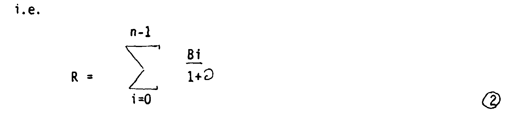
- Since each phase shift is related to the next smallest phase shift by the ratio β:1

- Substituting in ②

- Substituting using ①

- When the MSB is a maximum (Bn-1. (1+∂)) and the other units have a minimum value


- Rearranging


- Substituting in ④


or the ratio β and tolerable error ∂ for a given R/L
As shown below, for n = 6∂ (%) β R/L 0 2.00 63 5 1.91 47.1 10 1.83 36.1 15 1.76 28.3 20 1.69 22.7 25 1.64 18.5 and R/L β ∂(%) 63 2.00 0 50 1.93 4 40 1.86 8 31 1.78 13 - The figures of β given above are accurate only to two decimal places.
- One phase shifter according to the invention will now be described by way of example only.
- Referring to the figure, the phase shifter includes a control means comprising a circuit 7 and a look-up table 9. The circuit 7 receives an analogue signal representative of a desired phase shift to be presented to an input signal by units 1 to 6, each of which present a different phase shift value.
- The circuit 7 is an analogue to digital converter, which passes a five digit binary signal to the look-up table 9.
- In the look-up table 9, for each five digit signal, that combination of the six available phase shift values which most closely corresponds to the desired phase shift is selected.
- The phase shifter is designed to present a total phase shift of between 0° and 360°-L to the input signal and R/L =

- To achieve the same precision as would be achieved using five units in a conventional binary phase shifter with 0% error, the ratio R/L must equal 31.
- Thus the resolution L =

- if the percentage error to be tolerated is 13% from equation ①
- In this case β = 6

- Thus according to the invention, a phase shifter capable of presenting the above phase shift values to an input signal can produce a total phase shift of between 0° and 360° to the same resolution as would be achieved with a five unit phase shifter with 0% error, even if the percentage error in each phase shift value is 13%.
Claims (5)
- An electrical apparatus comprising control means (7, 9) and a number of units (1, 2, 3, 4, 5, 6) each of which is capable of presenting to an input signal a transfer function of a different value the transfer function values of the units being subject to possible error with respect to their nominal values whereby a desired selection of said units (1, 2, 3, 4, 5, 6) can be made so as to present to the input signal a total value of desired transfer function value within a predetermined range characterised in that the ratio between each nominal transfer function value and the next smallest nominal transfer function value is less than 2:1.
- An apparatus as claimed in Claim 1 wherein said ratio has the same value for each adjacent pair of transfer functions.
- An apparatus as claimed in Claim 2 wherein the ratio (β) is
 n is the number of units (1, 2, 3, 4, 5, 6)R is the range of value to be producedand L is the desired resolution.
 - An apparatus as claimed in any preceding claim wherein the value of the largest transfer function is chosen to equal to the median value of said range.
- An apparatus as claimed in any preceding claim wherein said transfer function is a phase shift.
Applications Claiming Priority (2)
| Application Number | Priority Date | Filing Date | Title |
|---|---|---|---|
| GB9124974A GB2261781B (en) | 1991-11-25 | 1991-11-25 | Electrical apparatus |
| GB9124974 | 1991-11-25 |
Publications (2)
| Publication Number | Publication Date |
|---|---|
| EP0544394A1 EP0544394A1 (en) | 1993-06-02 |
| EP0544394B1 true EP0544394B1 (en) | 1997-12-03 |
Family
ID=10705171
Family Applications (1)
| Application Number | Title | Priority Date | Filing Date |
|---|---|---|---|
| EP92308550A Expired - Lifetime EP0544394B1 (en) | 1991-11-25 | 1992-09-18 | Electrical apparatus |
Country Status (4)
| Country | Link |
|---|---|
| US (1) | US5327107A (en) |
| EP (1) | EP0544394B1 (en) |
| DE (1) | DE69223385T2 (en) |
| GB (1) | GB2261781B (en) |
Family Cites Families (7)
| Publication number | Priority date | Publication date | Assignee | Title |
|---|---|---|---|---|
| US3725686A (en) * | 1971-01-29 | 1973-04-03 | Hughes Aircraft Co | Polyphasor generation by vector addition and scalar multiplication |
| US4063250A (en) * | 1975-12-16 | 1977-12-13 | Electrospace Systems, Inc. | Beam and null switch step steerable antenna system |
| US4599585A (en) * | 1982-03-01 | 1986-07-08 | Raytheon Company | N-bit digitally controlled phase shifter |
| US4549152A (en) * | 1983-03-28 | 1985-10-22 | Rca Corporation | Broadband adjustable phase modulation circuit |
| US4841552A (en) * | 1988-04-04 | 1989-06-20 | Unisys Corporation | Digital phase shifter |
| US4994773A (en) * | 1988-10-13 | 1991-02-19 | Chen Tzu H | Digitally controlled monolithic active phase shifter apparatus having a cascode configuration |
| US5180998A (en) * | 1991-11-05 | 1993-01-19 | Itt Corporation | Switched transmission line phase shifter apparatus employing multiple jets |
-
1991
- 1991-11-25 GB GB9124974A patent/GB2261781B/en not_active Expired - Fee Related
-
1992
- 1992-09-18 EP EP92308550A patent/EP0544394B1/en not_active Expired - Lifetime
- 1992-09-18 DE DE69223385T patent/DE69223385T2/en not_active Expired - Fee Related
- 1992-09-24 US US07/950,804 patent/US5327107A/en not_active Expired - Fee Related
Non-Patent Citations (1)
| Title |
|---|
| Horowitz and Hill "The Art of Electronics" 2nd Edition, page 7 * |
Also Published As
| Publication number | Publication date |
|---|---|
| GB9124974D0 (en) | 1992-01-22 |
| DE69223385D1 (en) | 1998-01-15 |
| GB2261781B (en) | 1995-06-28 |
| EP0544394A1 (en) | 1993-06-02 |
| GB2261781A (en) | 1993-05-26 |
| US5327107A (en) | 1994-07-05 |
| DE69223385T2 (en) | 1998-04-02 |
Similar Documents
| Publication | Publication Date | Title |
|---|---|---|
| US4638303A (en) | Digital-analog converter | |
| US4503421A (en) | Digital to analog converter | |
| EP0372548B1 (en) | Successive comparison type analog-to-digital converting apparatus | |
| GB2102603A (en) | Controlled ram signal processor | |
| US2950469A (en) | Analogue to digital conversion apparatus | |
| GB1572765A (en) | Electric measuring apparatus | |
| EP0383151B1 (en) | Multistep flash analog to digital converter with voltage estimator | |
| KR900008048B1 (en) | Timming signal delay circuit | |
| GB2158318A (en) | Fading circuit for video signals | |
| HK78395A (en) | Method and circuit concerning the resolution of digital signals | |
| US5119098A (en) | Full flash analog-to-digital converter | |
| US4096475A (en) | Circuit for the conversion of a digital signal to an analog signal | |
| EP0480756B1 (en) | Digital-analog converter | |
| US5453743A (en) | Two-dimensional symmetric thermometer matrix decoder of digital/analog converter | |
| EP0200970B1 (en) | Digital-to-analog converter | |
| CA1161167A (en) | Setting circuit | |
| EP0544394A1 (en) | Electrical apparatus | |
| US4788528A (en) | Method and apparatus for high-resolution digitization of a signal | |
| GB2109135A (en) | Digital signal processing | |
| US4058807A (en) | Digital antilogarithmic converter circuit | |
| EP0702290A1 (en) | Digital dividing apparatus using a look-up table | |
| JPH03186077A (en) | digital mixer | |
| CN220067405U (en) | Digital-to-analog conversion device and signal processing apparatus | |
| EP0444890B1 (en) | Full flash analog-to-digital converter | |
| US6331828B1 (en) | Signal conversion method and signal converters |
Legal Events
| Date | Code | Title | Description |
|---|---|---|---|
| PUAI | Public reference made under article 153(3) epc to a published international application that has entered the european phase |
Free format text: ORIGINAL CODE: 0009012 |
|
| AK | Designated contracting states |
Kind code of ref document: A1 Designated state(s): DE FR |
|
| 17P | Request for examination filed |
Effective date: 19931201 |
|
| 17Q | First examination report despatched |
Effective date: 19960130 |
|
| GRAG | Despatch of communication of intention to grant |
Free format text: ORIGINAL CODE: EPIDOS AGRA |
|
| GRAH | Despatch of communication of intention to grant a patent |
Free format text: ORIGINAL CODE: EPIDOS IGRA |
|
| GRAH | Despatch of communication of intention to grant a patent |
Free format text: ORIGINAL CODE: EPIDOS IGRA |
|
| GRAA | (expected) grant |
Free format text: ORIGINAL CODE: 0009210 |
|
| AK | Designated contracting states |
Kind code of ref document: B1 Designated state(s): DE FR |
|
| ET | Fr: translation filed | ||
| REF | Corresponds to: |
Ref document number: 69223385 Country of ref document: DE Date of ref document: 19980115 |
|
| PLBE | No opposition filed within time limit |
Free format text: ORIGINAL CODE: 0009261 |
|
| 26N | No opposition filed | ||
| PGFP | Annual fee paid to national office [announced via postgrant information from national office to epo] |
Ref country code: FR Payment date: 20020910 Year of fee payment: 11 |
|
| PGFP | Annual fee paid to national office [announced via postgrant information from national office to epo] |
Ref country code: DE Payment date: 20020925 Year of fee payment: 11 |
|
| PG25 | Lapsed in a contracting state [announced via postgrant information from national office to epo] |
Ref country code: DE Free format text: LAPSE BECAUSE OF NON-PAYMENT OF DUE FEES Effective date: 20040401 |
|
| PG25 | Lapsed in a contracting state [announced via postgrant information from national office to epo] |
Ref country code: FR Free format text: LAPSE BECAUSE OF NON-PAYMENT OF DUE FEES Effective date: 20040528 |
|
| REG | Reference to a national code |
Ref country code: FR Ref legal event code: ST |