EP0544196A2 - Method of forming T-shape electrode - Google Patents
Method of forming T-shape electrode Download PDFInfo
- Publication number
- EP0544196A2 EP0544196A2 EP92119821A EP92119821A EP0544196A2 EP 0544196 A2 EP0544196 A2 EP 0544196A2 EP 92119821 A EP92119821 A EP 92119821A EP 92119821 A EP92119821 A EP 92119821A EP 0544196 A2 EP0544196 A2 EP 0544196A2
- Authority
- EP
- European Patent Office
- Prior art keywords
- resist layer
- exposure
- forming
- layer
- resist
- Prior art date
- Legal status (The legal status is an assumption and is not a legal conclusion. Google has not performed a legal analysis and makes no representation as to the accuracy of the status listed.)
- Ceased
Links
- 238000000034 method Methods 0.000 title claims description 23
- 239000000758 substrate Substances 0.000 claims abstract description 24
- 239000007772 electrode material Substances 0.000 claims description 9
- 230000005540 biological transmission Effects 0.000 claims description 6
- 238000005530 etching Methods 0.000 claims description 4
- 238000000151 deposition Methods 0.000 claims 1
- 230000001276 controlling effect Effects 0.000 description 5
- 230000015572 biosynthetic process Effects 0.000 description 4
- 238000010894 electron beam technology Methods 0.000 description 4
- 229910001218 Gallium arsenide Inorganic materials 0.000 description 2
- VYPSYNLAJGMNEJ-UHFFFAOYSA-N Silicium dioxide Chemical compound O=[Si]=O VYPSYNLAJGMNEJ-UHFFFAOYSA-N 0.000 description 2
- 235000010724 Wisteria floribunda Nutrition 0.000 description 2
- 238000007796 conventional method Methods 0.000 description 2
- 239000000463 material Substances 0.000 description 2
- 229920002120 photoresistant polymer Polymers 0.000 description 2
- 238000001020 plasma etching Methods 0.000 description 2
- 230000035945 sensitivity Effects 0.000 description 2
- 239000000126 substance Substances 0.000 description 2
- 238000005229 chemical vapour deposition Methods 0.000 description 1
- 229910052681 coesite Inorganic materials 0.000 description 1
- 238000004891 communication Methods 0.000 description 1
- 238000010276 construction Methods 0.000 description 1
- 229910052906 cristobalite Inorganic materials 0.000 description 1
- 230000007423 decrease Effects 0.000 description 1
- 238000013461 design Methods 0.000 description 1
- 238000000313 electron-beam-induced deposition Methods 0.000 description 1
- 230000008020 evaporation Effects 0.000 description 1
- 238000001704 evaporation Methods 0.000 description 1
- 230000005669 field effect Effects 0.000 description 1
- 238000010030 laminating Methods 0.000 description 1
- 238000012986 modification Methods 0.000 description 1
- 230000004048 modification Effects 0.000 description 1
- 239000003960 organic solvent Substances 0.000 description 1
- 229910021420 polycrystalline silicon Inorganic materials 0.000 description 1
- 229920001721 polyimide Polymers 0.000 description 1
- 229920005591 polysilicon Polymers 0.000 description 1
- 230000001105 regulatory effect Effects 0.000 description 1
- 239000000377 silicon dioxide Substances 0.000 description 1
- 235000012239 silicon dioxide Nutrition 0.000 description 1
- 229910052814 silicon oxide Inorganic materials 0.000 description 1
- 229910052682 stishovite Inorganic materials 0.000 description 1
- 229910052905 tridymite Inorganic materials 0.000 description 1
- 238000001039 wet etching Methods 0.000 description 1
Images


Classifications
-
- H—ELECTRICITY
- H01—ELECTRIC ELEMENTS
- H01L—SEMICONDUCTOR DEVICES NOT COVERED BY CLASS H10
- H01L29/00—Semiconductor devices adapted for rectifying, amplifying, oscillating or switching, or capacitors or resistors with at least one potential-jump barrier or surface barrier, e.g. PN junction depletion layer or carrier concentration layer; Details of semiconductor bodies or of electrodes thereof ; Multistep manufacturing processes therefor
- H01L29/66—Types of semiconductor device ; Multistep manufacturing processes therefor
- H01L29/66007—Multistep manufacturing processes
- H01L29/66075—Multistep manufacturing processes of devices having semiconductor bodies comprising group 14 or group 13/15 materials
- H01L29/66227—Multistep manufacturing processes of devices having semiconductor bodies comprising group 14 or group 13/15 materials the devices being controllable only by the electric current supplied or the electric potential applied, to an electrode which does not carry the current to be rectified, amplified or switched, e.g. three-terminal devices
- H01L29/66409—Unipolar field-effect transistors
- H01L29/66848—Unipolar field-effect transistors with a Schottky gate, i.e. MESFET
- H01L29/66856—Unipolar field-effect transistors with a Schottky gate, i.e. MESFET with an active layer made of a group 13/15 material
- H01L29/66863—Lateral single gate transistors
-
- G—PHYSICS
- G03—PHOTOGRAPHY; CINEMATOGRAPHY; ANALOGOUS TECHNIQUES USING WAVES OTHER THAN OPTICAL WAVES; ELECTROGRAPHY; HOLOGRAPHY
- G03F—PHOTOMECHANICAL PRODUCTION OF TEXTURED OR PATTERNED SURFACES, e.g. FOR PRINTING, FOR PROCESSING OF SEMICONDUCTOR DEVICES; MATERIALS THEREFOR; ORIGINALS THEREFOR; APPARATUS SPECIALLY ADAPTED THEREFOR
- G03F7/00—Photomechanical, e.g. photolithographic, production of textured or patterned surfaces, e.g. printing surfaces; Materials therefor, e.g. comprising photoresists; Apparatus specially adapted therefor
-
- H—ELECTRICITY
- H01—ELECTRIC ELEMENTS
- H01L—SEMICONDUCTOR DEVICES NOT COVERED BY CLASS H10
- H01L21/00—Processes or apparatus adapted for the manufacture or treatment of semiconductor or solid state devices or of parts thereof
- H01L21/02—Manufacture or treatment of semiconductor devices or of parts thereof
- H01L21/027—Making masks on semiconductor bodies for further photolithographic processing not provided for in group H01L21/18 or H01L21/34
- H01L21/0271—Making masks on semiconductor bodies for further photolithographic processing not provided for in group H01L21/18 or H01L21/34 comprising organic layers
- H01L21/0272—Making masks on semiconductor bodies for further photolithographic processing not provided for in group H01L21/18 or H01L21/34 comprising organic layers for lift-off processes
-
- H—ELECTRICITY
- H01—ELECTRIC ELEMENTS
- H01L—SEMICONDUCTOR DEVICES NOT COVERED BY CLASS H10
- H01L21/00—Processes or apparatus adapted for the manufacture or treatment of semiconductor or solid state devices or of parts thereof
- H01L21/02—Manufacture or treatment of semiconductor devices or of parts thereof
- H01L21/027—Making masks on semiconductor bodies for further photolithographic processing not provided for in group H01L21/18 or H01L21/34
- H01L21/0271—Making masks on semiconductor bodies for further photolithographic processing not provided for in group H01L21/18 or H01L21/34 comprising organic layers
- H01L21/0273—Making masks on semiconductor bodies for further photolithographic processing not provided for in group H01L21/18 or H01L21/34 comprising organic layers characterised by the treatment of photoresist layers
- H01L21/0274—Photolithographic processes
-
- H—ELECTRICITY
- H01—ELECTRIC ELEMENTS
- H01L—SEMICONDUCTOR DEVICES NOT COVERED BY CLASS H10
- H01L21/00—Processes or apparatus adapted for the manufacture or treatment of semiconductor or solid state devices or of parts thereof
- H01L21/02—Manufacture or treatment of semiconductor devices or of parts thereof
- H01L21/04—Manufacture or treatment of semiconductor devices or of parts thereof the devices having at least one potential-jump barrier or surface barrier, e.g. PN junction, depletion layer or carrier concentration layer
- H01L21/18—Manufacture or treatment of semiconductor devices or of parts thereof the devices having at least one potential-jump barrier or surface barrier, e.g. PN junction, depletion layer or carrier concentration layer the devices having semiconductor bodies comprising elements of Group IV of the Periodic System or AIIIBV compounds with or without impurities, e.g. doping materials
- H01L21/28—Manufacture of electrodes on semiconductor bodies using processes or apparatus not provided for in groups H01L21/20 - H01L21/268
- H01L21/283—Deposition of conductive or insulating materials for electrodes conducting electric current
- H01L21/285—Deposition of conductive or insulating materials for electrodes conducting electric current from a gas or vapour, e.g. condensation
- H01L21/28506—Deposition of conductive or insulating materials for electrodes conducting electric current from a gas or vapour, e.g. condensation of conductive layers
- H01L21/28575—Deposition of conductive or insulating materials for electrodes conducting electric current from a gas or vapour, e.g. condensation of conductive layers on semiconductor bodies comprising AIIIBV compounds
- H01L21/28587—Deposition of conductive or insulating materials for electrodes conducting electric current from a gas or vapour, e.g. condensation of conductive layers on semiconductor bodies comprising AIIIBV compounds characterised by the sectional shape, e.g. T, inverted T
-
- H—ELECTRICITY
- H01—ELECTRIC ELEMENTS
- H01L—SEMICONDUCTOR DEVICES NOT COVERED BY CLASS H10
- H01L29/00—Semiconductor devices adapted for rectifying, amplifying, oscillating or switching, or capacitors or resistors with at least one potential-jump barrier or surface barrier, e.g. PN junction depletion layer or carrier concentration layer; Details of semiconductor bodies or of electrodes thereof ; Multistep manufacturing processes therefor
- H01L29/66—Types of semiconductor device ; Multistep manufacturing processes therefor
- H01L29/66007—Multistep manufacturing processes
- H01L29/66075—Multistep manufacturing processes of devices having semiconductor bodies comprising group 14 or group 13/15 materials
- H01L29/66227—Multistep manufacturing processes of devices having semiconductor bodies comprising group 14 or group 13/15 materials the devices being controllable only by the electric current supplied or the electric potential applied, to an electrode which does not carry the current to be rectified, amplified or switched, e.g. three-terminal devices
- H01L29/66409—Unipolar field-effect transistors
- H01L29/66446—Unipolar field-effect transistors with an active layer made of a group 13/15 material, e.g. group 13/15 velocity modulation transistor [VMT], group 13/15 negative resistance FET [NERFET]
- H01L29/66462—Unipolar field-effect transistors with an active layer made of a group 13/15 material, e.g. group 13/15 velocity modulation transistor [VMT], group 13/15 negative resistance FET [NERFET] with a heterojunction interface channel or gate, e.g. HFET, HIGFET, SISFET, HJFET, HEMT
Definitions
- the present invention relates to a method of forming a T-shape electrode.
- Microwave FETs including MESFETs, HEMFETs and the like used in a microwave circuit have been desired to have a short gate length in order to suppress noise.
- the gate length be shorter, the gate resistance would become higher, and accordingly, it is very difficult to suppress noise in a microwave FET.
- a gate electrode having a T-like cross-sectional shape which can provide not only its shorten gate length but also its reduced gate resistance has been proposed.
- TECHNICAL REPORT ED-90-92 published by the Association of Electronic Date Communication, pages 37 to 43, discloses a conventional method of forming T-shape gate electrode.
- Figs. 6A to 6D are sectional views for explaining the process steps for forming a conventional T-shape electrode, disclosed in the above-mentioned document.
- a lower resist layer 12 having a low sensitivity and a high resolution, and an upper resist layer 14 having a high sensitivity are formed on a GaAs substrate 10, successively.
- the upper and lower resist layers 14, 12 are exposed by an electron beam type direct plotting apparatus, and thereafter, they are developed so as to form an aperture 16 for exposing a surface of the GaAs substrate 10, through the resist layers 14, 12.
- the upper resist layer 14 is dissolved by a developer largely in comparison with lower resist layer 12 even though both upper and lower resist layers 14,12 are exposed at an equal exposure value, and accordingly, the aperture 16 having a T-like cross-sectional shape can be formed.
- a material layer 18 for forming a gate electrode is deposited on the surface of the substrate 10 and the lower resist layer 12 which are exposed through the aperture 16.
- the upper and lower resist layers 12,14 are removed so as to a gate electrode 20 having a T-like cross-sectional shape is obtained.
- the gate length can be effectively shorten by narrowing the width of the base part of the gate electrode 20, and further, the resistance of the gate electrode 20 can be reduced by widening the width of the head part of the gate electrode.
- the electron beam type direct plotting apparatus scans a resist layer with an electron beam so as to depict the shape of a gate electrode thereon for exposure thereof, a long time is consumed for depicting the gate electrode, causing lowering of the productivity thereof.
- one object of the present invention is to provide a method of forming a T-shape electrode, in particular, a T-shape gate electrode with the use of a projection exposure process.
- a T-shape electrode forming method is, according to the present invention, characterized by the steps of: forming a lower mask layer for forming an electrode over a substrate; applying a first resist layer of a negative type over the lower mask layer, exposing the first resist layer with the use of an exposure mask incorporating a phase shifter having an edge so as to form a first unexposed part in fine line corresponding to the edge of the phase shifter, on the first resist layer, developing the first resist layer so as to remove the first unexposed part in order to form a first rest pattern, etching the lower mask layer through the first resist pattern so as to form an aperture in slit for exposing the substrate, in the lower mask layer, removing the first resist pattern, and applying a second resist layer of a negative type over the lower mask layer in which the aperture have been formed, exposing the second resist layer with the use of the exposure mask at an exposure value which is less than that used for the first resist layer, so as to form a second une
- phase of light transmitted through the above-mentioned phase shifter on the exposure mask according to the present invention differs from that of light not transmitted therethrough by about 180 deg.
- the intensity of light irradiated onto a part of the negative resist layer which corresponds to the edge of the phase shifter (which will be denoted as edge corresponding part) is weakened due to the interference of light.
- the exposure of the edge corresponding part can be regulated to a degree such that the edge corresponding part does not loose its behavior with which it can be dissolved by the developer, an unexposed part which has not been substantially exposed can be formed in the edge corresponding part.
- an unexposed part having an extremely narrow width is formed in the edge corresponding part. That is, an unexposed part having a width of less than 0.25 ⁇ m can be formed although this numerical value is not absolutely essential.
- the width (area) of the unexposed part formed in the edge corresponding part can be controlled by an exposure value. The larger the exposure value, the smaller the width of the unexposed part becomes, that is, the smaller the exposure value, the larger the width of the unexposed part becomes. Accordingly, even though the first and second resist layers are exposed by a common exposure mask, the width of an unexposed part formed on the second resist layer can be made to be wider than that of an exposed part formed on the first resist layer, by controlling the exposure value.
- an exposure mask or a first exposure mask incorporating thereon a phase shifter, for forming the plan view shape of the T-shape electrode into a desired pattern for a T-like cross-sectional shape gate electrode
- another exposure mask or a second exposure mask incorporating a light shield part at a position corresponding to an electrode pattern part on the edge of the phase shifter and a light transmission part at a position corresponding to a non-electrode pattern part on the edge of the phase shifter, is also used.
- Fig. 1A is a plan view illustrating the general configuration of the first exposure mask used in this embodiment
- Fig. 1B is a sectional view taken along Line IB-IB in Fig. 1A.
- the first exposure mask 22 is formed by arranging on a light transmission section 28 in a first light transmissive substrate both a first light shield part 24 used for forming a gate electrode pad and a phase shifter 26 used for forming a T-shape gate electrode.
- the edge 26a of phase shifter 26 is extended into an area on the light transmission section 28 where the first light shield part 24 is not provided.
- the plan view shape of the first shield part 24 is rectangular.
- a first side extending in the Y-axis direction has a length W1 and a second side extending in the X-axis direction orthogonal to the first side has a length (W2 + 2W X ), where W1 is a value which is obtained by multiplying an absolute size of a side of the gate electrode pad extending in the X-axis direction on design, with the reciprocal of a reduction ratio t given by a projection exposure apparatus, and W2 is a value which is obtained by multiplying an absolute size of a side of the gate electrode pad extending in the Y-axis direction, with the reciprocal of the reduction ratio t given by the projection exposure apparatus.
- W X is an estimated positional shift in the X-axial direction between the first exposure mask 22 and a second exposure mask 30 which will be explained later. That is, the left end of the first light shield part 24 is spaced from a position corresponding to the position of the left end of the gate electrode pad on the first exposure mask 22, by W X in the X-axis direction in Fig. 1A. Further, the right end of the first shield part 24 is spaced from a position corresponding to the right end of the gate electrode pad on the first exposure mask 22, by W X in the X-axis direction in Fig. 1A.
- Fig. 2A is a plan view showing the general construction of the second exposure mask
- Fig. 2B is a sectional view taken along line IIB-IIB.
- the second exposure 30 in this embodiment is formed by arranging on a second light transmission part 36 in a second light transmissive substrate a second light shield part 32 for forming a gate electrode pad, and a third light shield part 34 for forming a T-shape gate electrode.
- the second light shield part 32 is located at a position corresponding to the first light shield part 24 on the first light exposure mask 22, and the third light shield part 34 is located at a position corresponding to the gate electrode pattern part on the edge 26a of the first exposure mask 22, these light shield parts 32, 34 being connected together.
- an area in the light transmission part 36 where the second and third light shield parts 32, 34 are not present is provided at a position corresponding to the non-electrode pattern part on the edge 26a of the first exposure mask 22.
- the plan view shape of the second light shield part 32 is rectangular.
- a second side of this light shield part 32, extending in the X-axis direction, has a length W2 and a first side thereof extending in the Y-axis direction orthogonal to the second side has a length (W1 + 2W Y ) where W Y is an estimated positional shift in the Y-axis direction between the first exposure mask 22 and the second exposure mask 30, that is, the upper end of the second light shield part 32 is spaced from the position corresponding to the upper end of the gate electrode pad on the second exposure mask 30 by W Y in the Y-axis direction as shown in Fig. 2A. Further, the lower end of the second light shield part 32 is shifted from the position corresponding to the lower end of the gate electrode pad on the second exposure mask 32 on the second exposure mask 30 by W Y .
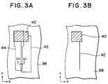
- Figs. 3A and 3B show a plan view illustrating the unexposed part formed in the resist layer through the first and second exposures.
- a light shield part 40 for forming a pad is formed in a part of the resist layer 38 corresponding to the first light shield part 24 while an exposed part 42 for forming a gate electrode is formed in a part of the resist layer 38 corresponding to the edge of the phase shifter 26.
- the second exposure mask 30 are set so as to carry out the second exposure.
- the second exposure mask 30 is set so as to be shifted in the X-axial direction in such a way that the left side of the second light shield part 32 on the second exposure mask 30 is superposed with the left side of the first light shield part 24 on the first exposure mask 22.
- a light shield area 44 which is formed on the resist layer 38 by the second and third light shield parts 32, 34 on the second exposure mask 30 is shown in Fig. 3A.
- the nonelectrode pattern part is exposed while the gate electrode pattern part in the unexposed part 42 for forming the gate electrode is prevented from being exposed during the second exposure, as shown in Fig. 3B.
- the lengths of sides of the unexposed electrode pattern part for forming the pad which extend in the X- and Y-axial directions, can be set to predetermined designed sizes (W1 x t) and (W2 x t).
- the unexposed parts 40, 42 having patterns similar to those shown in Fig. 3B can be formed.
- a gate electrode pad and a gate electrode having plan view shapes equivalent to, for example, those of the unexposed parts 40, 42 shown in Fig. 3B are formed by the twice exposures using the first exposure mask 22 and the second exposure mask 30.
- Figs. 4A to 4L are sectional views along line III-III in Fig. 3A, for explaining these process steps which are particularly directed to the formation of the T-shape gate electrode.
- a substrate 46 on which a T-shape gate electrode is to be formed is prepared, as shown in Fig. 4A.
- the substrate 46 incorporates an active layer (which is not shown) for a field-effect transistor, and further incorporates a source electrode (ohmic electrode) and a drain electrode (ohmic electrode) formed on the active layer although they are not shown.
- an SiN film having a thickness of about 1,000 ⁇ as a lower mask layer 48 is formed on the substrate 46 by using, for example, a plasma chemical vapor deposition (PCVD) process, as shown in Fig. 4B.
- PCVD plasma chemical vapor deposition
- a film other than the SiN film can be formed as the lower mask layer 48.
- an inorganic insulating film such as an SiO2 film, a SiON film, a resist which does not mingle with a negative type resist, and accordingly does not change the properties of the negative type resist
- an organic insulating film such as a polyimide film or the like, a conductive film such as a polysilicon film or the like can be used.
- a negative first resist layer 50 having a thickness of about 0.7 ⁇ m is applied over the lower mask layer 48.
- FSMR Fuji Chemical Manufacturing Co., Ltd
- the first resist layer 50 is exposed with the use of the first exposed mask 22 incorporating the phase shifter 26 so as to form a thin line-like first unexposed part 50b corresponding to the edge 26a of the phase shifter 26 in the first resist layer 50.
- an i-line stepper apparatus RA101VLII manufactured by Hitachi Manufacturing Co., Ltd is used as a stepper so as to set the exposure value for the first resist layer 50 is set to about 250 mJ.cm ⁇ 2.
- an exposed part (which is not shown) for forming a pad, and an exposed part 50b for forming a gate electrode are formed in the first resist layer 50.
- the phase of exposure light having transmitted through the phase shifter 26 on the first exposure mask 22 is shifted from that of exposure light having not transmitted through the phase shifter 26 on the first exposure mask 22 by 180 deg. by controlling, for example, the thickness of the phase shifter 26.
- the exposure value to a part of the first resist layer 50 corresponding to the edge of the phase shifter 26 is reduced to such a degree that the dissolving characteristic of the edge corresponding part with respect to the developer is not changed, and accordingly, the thin line-like unexposed part 50b which is not substantially exposed is formed in this edge corresponding part.
- the first resist layer 50 is exposed with the use of the second exposure mask 30 so as to form an exposed part (which is not shown) for forming a pad having a predetermined pattern, and an unexposed part 50b for forming a gate electrode in the first resist layer 50.
- the unexposed parts 40, 42 shown in Fig. 3(B) the unexposed part for forming a pad having a predetermined shape and the unexposed part 50b for forming a gate electrode having a predetermined shape are formed in the first resist layer 50.
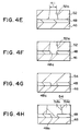
- the first resist layer 50 is developed so as to remove the unexposed part 50b in order to form a first resist patter 52.
- an aperture (which is not shown) for forming a pad, and an aperture 52a for forming an electrode are formed in the first resist layer 50 so as to obtain the first resist pattern 52 having these apertures.
- the lower mask layer 48 is in part exposed through the aperture for forming a pad and the aperture for forming a gate electrode in the first resist pattern 52.
- the length H1 of the aperture 52 in the longitudinal direction of the gate electrode can be set to about 0.15 ⁇ m.
- the longitudinal direction of the gate electrode is orthogonal to the edge of the phase shifter 26.
- the lower mask layer 48 is etched through the intermediary of the first resist pattern 52 so as to form a thin line-like aperture 48a for exposing the substrate 46 in the lower mask layer 48.
- the lower mask layer is subjected to anisotropic etching such as reactive ion etching so as to form an aperture (which is not shown) for forming a pad and the aperture 48a for forming a gate electrode.
- a negative type second resist layer 54 having a thickness of about 0.7 ⁇ m is applied over the lower mask layer 48 formed therein with the aperture 48.
- FSMR manufactured by Fuji Chemical Manufacturing Co., Ltd
- the second resist layer 54 is exposed by an exposure value which is less than that for the first resist layer 51, with the use of the first exposure mask 22 so as to form a thin line-like second unexposed part 54b which is laid above the aperture 48a formed in the lower mask layer and which is wider than this aperture 48a, in the second resist layer 54.
- the stepper used for exposing the first resist layer 51 is used so as to set the exposure value to, for example, about 100 mJ.cm ⁇ 2 for exposing the second resist layer 54 in order to form an unexposed part (which is not shown) for forming a pad and the unexposed part 54b for forming a gate electrode in the second resist layer 54.
- the unexposed part for forming a pad and the unexposed part 54b for forming a gate electrode are formed so that they are superposed with the aperture for forming a pad and the aperture 48a for forming a gate electrode in the lower mask layer 48 as viewed in a plan view. If the exposure value for the second resist layer 54 is set to be smaller than that for the first resist layer 50, the plan view shape of the unexposed part for forming a pad, in the second resist layer 54 is substantially the same as that of the unexposed part in the first resist layer 50, corresponding to the first light shield part 24.
- the unexposed part 54 for forming a gate electrode in the second resist layer 54 is wider than the unexposed part for forming a gate electrode, corresponding to the edge of the phase shifter 26, in the first resist layer 50, as viewed in a plan view.
- the length H2, in the longitudinal direction of the gate electrode, of an aperture which is formed in the second resist layer 54 by developing and removing the unexposed part for forming a gate electrode is longer than the length H1 of the aperture 52a for forming a gate electrode, formed in the first resist layer 50. If the exposure value for the second resist layer 55 is set to about 100 mJ.cm ⁇ 2, the length H2 of the aperture in the second resist layer 54 can be about a 0.35 ⁇ m. This reason will be explained with reference to Fig. 5.
- Fig. 5 is a graph showing the relationship between the resist exposure value (dose) and the width of an aperture formed in the part corresponding to the edge of the phase shifter in such a case that the resist layer is exposed by the first exposure mask incorporating the phase shifter.
- the ordinate gives the length H2 ( ⁇ m) of the aperture formed in the part of the resist layer corresponding to the edge of the phase shifter, in the direction orthogonal to the edge of the phase shifter (the longitudinal direction of the gate electrode in this embodiment), and the abscissa gives the exposure strength (mJ.cm ⁇ 2) for the resist layer.
- the relationship between the width of the unexposed part and the exposure strength is detailed in an document, "IEDM Technical Digest", 1990, pages 33.3.1 to 33.3.4.
- the length H2 of the aperture formed by developing in the part of the resist layer corresponding to the edge of the phase shifter increases as the exposure value for the resist layer decreases.
- the length H2 of the aperture in the second resist layer 54 can be wider than the length H1 of the aperture in the first resist layer 50 by setting the exposure value for the second resist layer 54 to a value which is smaller than that for the first resist layer 50. Since the length H3, in the longitudinal direction of the gate electrode, of the aperture for forming a gate electrode in the lower mask layer 48 is equal to that aperture length H1, the length H2 of the aperture in the second resist layer 54 is longer than the length H3 of the aperture in the lower mask layer 48.
- the second resist layer 54 is exposed with the use of the second exposure mask 30 so as to form an unexposed part (which is not shown) having a predetermined pattern for forming a pad and an unexposed part 54b for forming a gate electrode in the second resist layer 54.
- an unexposed part (which is not shown) having a predetermined pattern for forming a pad and an unexposed part 54b for forming a gate electrode in the second resist layer 54.
- the unexposed part having a predetermined shape for forming a pad and the unexposed part 54b having a predetermined shape for forming a gate electrode are formed in the second resist layer 54.
- the second resist layer 54 is developed so as to remove the second unexposed part 54b in order to form a second resist pattern 56 as an upper mask layer for forming an electrode.
- the second resist layer 54 by developing the second resist layer 54 so as to form an aperture (which is not shown) for forming a pad and an aperture 56a for forming a gate electrode in the second resist layer 54, and therefore, the second resist pattern 56 having these apertures is obtained.
- the substrate 46 is in part exposed through the apertures for forming a pad and a gate electrode in the second resist pattern 56 and the apertures for forming a pad and a gate electrode in the lower mask layer 48.
- the second resist pattern will be hereinbelow denoted as an upper mask layer 56.
- a recess 57 is formed in the substrate 46 in a part which is exposed through the upper and lower mask layers 56, 48.
- the recess 57 having about a depth of about 1,000 ⁇ is formed by for example, wet-etching.
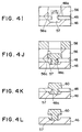
- the electrode material 58 has a double layer structure which is composed of a Ti film and an A1 film deposited in that order as view from the substrate 46, and the electrode material 58 having the double layer structure is used for an electrode material for forming a gate electrode and a pad. Further, by use of an electron beam deposition under evaporation, a Ti film having a thickness of about 200 ⁇ and an A1 film having a thickness of about 500 ⁇ are deposited successively so as to form the electrode material 58 (Fig. 4J).
- the upper mask layer 56 is removed so as to lift off the electrode material 58.
- the electrode material 58 remaining on the substrate 46 constitutes a gate electrode 60 and a pad (which is not shown) as shown in Fig. 4K.
- the aperture for forming a gate electrode formed in the upper mask layer 56 is wider than that formed in the lower mask layer 48 as viewed in a plan view, and accordingly, the gate electrode 60 can have a T-like sectional shape.
- the lower mask layer 48 is removed from the substrate 46 by, for example, plasma etching (Fig. 4L) so as to complete the formation of the gate electrode 60 and the pad.
- the present invention should not be limited to the above-mentioned embodiment, but various modification can be made suitably to the configuration of the several components, the shape, the materials to be used, the numerical condition, the arrangement positions and the like.
- the method of forming a T-shape electrode, according to the present invention can be used for forming T-shape electrodes for various kinds of electric circuit elements.
- control electrodes for MESFETs, MEMTs, MOSFETs diodes or bipolar transistors can be formed as T-shape electrodes having a fine width.
- the method of forming a gate electrode and a pad should not be limited to the above-mentioned embodiment.
- the gate electrode and the pad can be formed in respective processes. That is, the light shield parts for forming a pad can be eliminated from the first and second exposure masks for forming a gate electrode in order to form the gate electrode. Further, by forming the gate electrode and the pad in respective processes, a recess is formed in the substrate in an area in which the gate electrode is to be formed. Further, a T-shape electrode other than the gate electrode can be formed so that the T-shape electrode is formed by using only the first exposure mask without using the second exposure mask.
- the phase of exposure light which has transmitted through the phase shifter on the exposure mask differs from that of exposure light which has not transmitted through the phase shifter by about 180 deg in a projection exposure process
- the intensity of light irradiated to the part of the negative resist layer corresponding to the edge of the phase shifter that is, the edge corresponding part
- the exposure to the edge corresponding part can be restrained up to a degree such that its dissolving property with respect to the developer is not loosened, an unexposed part which is not substantially exposed can be formed in the edge corresponding part. Further, a fine line-like unexposed part can be formed in this edge corresponding part.
- an unexposed part in the second resist layer can be wider than an unexposed part in the first resist layer, even with the use of a common exposure mask, by controlling the exposure value. Accordingly, instead of a electron beam type plotting apparatus, by using a projection exposure process, and in particular, by using reduced scale exposure process, a T-shape electrode can be formed, thereby it is possible to enhance the productivity. Further, even with the one and the same exposure mask, the width of the unexposed part in the first resist layer can be changed into a desired value by controlling the exposure strength, and accordingly, T-shape electrode having various widths can be formed by using the technique of controlling the exposure.
Abstract
A lower mask layer and a first resist layer are formed on a substrate. The first resister is exposed with the use of an exposure mask having a phase shifter. A part of the first resist layer corresponding to the edge of the phase shifter becomes an unexposed part so that an aperture in slit is formed in the first resist layer by developing. The first mask layer is etched through said first resist layer so as to form an aperture for forming a gate electrode. A second resist layer as an upper mask layer is formed over the lower mask layer. The second resist layer is exposed with the use of the same exposure mask, and is then developed. By setting the exposure strength to a value lower than an exposure strength for exposure to the first resist layer, a wider aperture is formed in the second resist layer. With the use of the lower mask layer having the narrower aperture and the upper mask layer having the wider upper mask layer, a T-shape electrode is formed.
Description
- The present invention relates to a method of forming a T-shape electrode.
- Microwave FETs including MESFETs, HEMFETs and the like used in a microwave circuit have been desired to have a short gate length in order to suppress noise. However, should the gate length be shorter, the gate resistance would become higher, and accordingly, it is very difficult to suppress noise in a microwave FET. Accordingly, a gate electrode having a T-like cross-sectional shape, which can provide not only its shorten gate length but also its reduced gate resistance has been proposed. For example, TECHNICAL REPORT ED-90-92 published by the Association of Electronic Date Communication, pages 37 to 43, discloses a conventional method of forming T-shape gate electrode.
- Figs. 6A to 6D are sectional views for explaining the process steps for forming a conventional T-shape electrode, disclosed in the above-mentioned document.
- In the conventional forming method, at first, as shown in Fig. 6A, a
lower resist layer 12 having a low sensitivity and a high resolution, and anupper resist layer 14 having a high sensitivity are formed on aGaAs substrate 10, successively. - Then, as shown in Fig. 6B, the upper and
lower resist layers aperture 16 for exposing a surface of theGaAs substrate 10, through theresist layers upper resist layer 14 is dissolved by a developer largely in comparison withlower resist layer 12 even though both upper andlower resist layers aperture 16 having a T-like cross-sectional shape can be formed. - Next, as shown in Fig. 6C, a
material layer 18 for forming a gate electrode is deposited on the surface of thesubstrate 10 and thelower resist layer 12 which are exposed through theaperture 16. - Further, as shown in Fig. 6D, the upper and
lower resist layers gate electrode 20 having a T-like cross-sectional shape is obtained. The gate length can be effectively shorten by narrowing the width of the base part of thegate electrode 20, and further, the resistance of thegate electrode 20 can be reduced by widening the width of the head part of the gate electrode. - However, since the electron beam type direct plotting apparatus scans a resist layer with an electron beam so as to depict the shape of a gate electrode thereon for exposure thereof, a long time is consumed for depicting the gate electrode, causing lowering of the productivity thereof.
- Accordingly, in order to solve the above-mentioned problems inherent to the conventional method, one object of the present invention is to provide a method of forming a T-shape electrode, in particular, a T-shape gate electrode with the use of a projection exposure process. In order to achieve the above-mentioned object, a T-shape electrode forming method is, according to the present invention, characterized by the steps of:
forming a lower mask layer for forming an electrode over a substrate;
applying a first resist layer of a negative type over the lower mask layer,
exposing the first resist layer with the use of an exposure mask incorporating a phase shifter having an edge so as to form a first unexposed part in fine line corresponding to the edge of the phase shifter, on the first resist layer,
developing the first resist layer so as to remove the first unexposed part in order to form a first rest pattern,
etching the lower mask layer through the first resist pattern so as to form an aperture in slit for exposing the substrate, in the lower mask layer,
removing the first resist pattern, and applying a second resist layer of a negative type over the lower mask layer in which the aperture have been formed,
exposing the second resist layer with the use of the exposure mask at an exposure value which is less than that used for the first resist layer, so as to form a second unexposed part in fine line which is laid above the aperture and which is wider than the aperture, in the second resist layer,
developing the second resist layer so as to remove the second unexposed part in order to from a second resist pattern as an upper layer mask for forming an electrode, and
laminating an electrode material on the substrate through the upper and lower mask layers, and thereafter, removing the upper and lower mask layers. - The phase of light transmitted through the above-mentioned phase shifter on the exposure mask according to the present invention differs from that of light not transmitted therethrough by about 180 deg. By the projection exposure of a negative type resist layer with the use of this exposure mask, the intensity of light irradiated onto a part of the negative resist layer which corresponds to the edge of the phase shifter (which will be denoted as edge corresponding part) is weakened due to the interference of light.
- Accordingly, since the exposure of the edge corresponding part can be regulated to a degree such that the edge corresponding part does not loose its behavior with which it can be dissolved by the developer, an unexposed part which has not been substantially exposed can be formed in the edge corresponding part. Further, an unexposed part having an extremely narrow width is formed in the edge corresponding part. That is, an unexposed part having a width of less than 0.25 µm can be formed although this numerical value is not absolutely essential. Further, the width (area) of the unexposed part formed in the edge corresponding part can be controlled by an exposure value. The larger the exposure value, the smaller the width of the unexposed part becomes, that is, the smaller the exposure value, the larger the width of the unexposed part becomes. Accordingly, even though the first and second resist layers are exposed by a common exposure mask, the width of an unexposed part formed on the second resist layer can be made to be wider than that of an exposed part formed on the first resist layer, by controlling the exposure value.
-
- Figs. 1A and 1B are plan and sectional views illustrating a first exposure mask used for forming a T-shape electrode according to the present invention, respectively;
- Figs. 2A and 2B are plan and sectional views illustrating a second exposure mask used for forming a T-shape electrode, respectively;
- Figs. 3A and 3B are plan views illustrating an unexposed part on a resist layer after exposure with the use of the first and second exposure mask, respectively;
- Figs. 4A to 4L are sectional views for explaining the process of forming a T-shape electrode according to the present invention, respectively;
- Fig. 5 is a graph showing the relationship between the exposure strength and the aperture width formed in the resist after exposure with the use of the first exposure mask; and
- Figs. 6A to 6D are sectional views illustrating a conventional T-shape electrode forming method, respectively.
- Explanation will be made hereinbelow of one embodiment form of the present invention. In this embodiment, the simultaneous formation of both T-shape gate electrode and gate electrode pad is exemplified.
- In this embodiment, in addition to an exposure mask (or a first exposure mask) incorporating thereon a phase shifter, for forming the plan view shape of the T-shape electrode into a desired pattern for a T-like cross-sectional shape gate electrode, another exposure mask (or a second exposure mask) incorporating a light shield part at a position corresponding to an electrode pattern part on the edge of the phase shifter and a light transmission part at a position corresponding to a non-electrode pattern part on the edge of the phase shifter, is also used.
- Fig. 1A is a plan view illustrating the general configuration of the first exposure mask used in this embodiment, and Fig. 1B is a sectional view taken along Line IB-IB in Fig. 1A. The
first exposure mask 22 is formed by arranging on alight transmission section 28 in a first light transmissive substrate both a firstlight shield part 24 used for forming a gate electrode pad and aphase shifter 26 used for forming a T-shape gate electrode. Theedge 26a ofphase shifter 26 is extended into an area on thelight transmission section 28 where the firstlight shield part 24 is not provided. - The plan view shape of the
first shield part 24 is rectangular. A first side extending in the Y-axis direction has a length W₁ and a second side extending in the X-axis direction orthogonal to the first side has a length (W₂ + 2WX), where W₁ is a value which is obtained by multiplying an absolute size of a side of the gate electrode pad extending in the X-axis direction on design, with the reciprocal of a reduction ratio t given by a projection exposure apparatus, and W₂ is a value which is obtained by multiplying an absolute size of a side of the gate electrode pad extending in the Y-axis direction, with the reciprocal of the reduction ratio t given by the projection exposure apparatus. - Further, WX is an estimated positional shift in the X-axial direction between the
first exposure mask 22 and asecond exposure mask 30 which will be explained later. That is, the left end of the firstlight shield part 24 is spaced from a position corresponding to the position of the left end of the gate electrode pad on thefirst exposure mask 22, by WX in the X-axis direction in Fig. 1A. Further, the right end of thefirst shield part 24 is spaced from a position corresponding to the right end of the gate electrode pad on thefirst exposure mask 22, by WX in the X-axis direction in Fig. 1A. - Fig. 2A is a plan view showing the general construction of the second exposure mask, and Fig. 2B is a sectional view taken along line IIB-IIB. The
second exposure 30 in this embodiment is formed by arranging on a secondlight transmission part 36 in a second light transmissive substrate a secondlight shield part 32 for forming a gate electrode pad, and a thirdlight shield part 34 for forming a T-shape gate electrode. The secondlight shield part 32 is located at a position corresponding to the firstlight shield part 24 on the firstlight exposure mask 22, and the thirdlight shield part 34 is located at a position corresponding to the gate electrode pattern part on theedge 26a of thefirst exposure mask 22, theselight shield parts light transmission part 36 where the second and thirdlight shield parts edge 26a of thefirst exposure mask 22. - The plan view shape of the second
light shield part 32 is rectangular. A second side of thislight shield part 32, extending in the X-axis direction, has a length W₂ and a first side thereof extending in the Y-axis direction orthogonal to the second side has a length (W₁ + 2WY) where WY is an estimated positional shift in the Y-axis direction between thefirst exposure mask 22 and thesecond exposure mask 30, that is, the upper end of the secondlight shield part 32 is spaced from the position corresponding to the upper end of the gate electrode pad on thesecond exposure mask 30 by WY in the Y-axis direction as shown in Fig. 2A. Further, the lower end of the secondlight shield part 32 is shifted from the position corresponding to the lower end of the gate electrode pad on thesecond exposure mask 32 on thesecond exposure mask 30 by WY. - Next, explanation will be made of an unexposed part (latent image) formed in a resist layer through twice exposures with the use of the first and second exposure masks 22, 30.
- Consideration is made of such a case that the resist layer is exposed with the use of the first exposure mask 22 (first exposure), and then, is exposed by the second exposure mask 30 (second exposure). Figs. 3A and 3B show a plan view illustrating the unexposed part formed in the resist layer through the first and second exposures.
- As shown in Fig. 3A, through the first exposure, a
light shield part 40 for forming a pad is formed in a part of the resistlayer 38 corresponding to the firstlight shield part 24 while an exposedpart 42 for forming a gate electrode is formed in a part of the resistlayer 38 corresponding to the edge of thephase shifter 26. - After the first exposure, the
second exposure mask 30 are set so as to carry out the second exposure. At this stage, as shown in Fig. 3A, for example, thesecond exposure mask 30 is set so as to be shifted in the X-axial direction in such a way that the left side of the secondlight shield part 32 on thesecond exposure mask 30 is superposed with the left side of the firstlight shield part 24 on thefirst exposure mask 22. Alight shield area 44 which is formed on the resistlayer 38 by the second and thirdlight shield parts second exposure mask 30 is shown in Fig. 3A. In this case, since the estimated positional shift upon the mask setting is considered to the widths, in the X-axial direction, of the second and thirdlight shield parts second exposure mask 30, the nonelectrode pattern part is exposed while the gate electrode pattern part in theunexposed part 42 for forming the gate electrode is prevented from being exposed during the second exposure, as shown in Fig. 3B. Further, the lengths of sides of the unexposed electrode pattern part for forming the pad, which extend in the X- and Y-axial directions, can be set to predetermined designed sizes (W₁ x t) and (W₂ x t). Even though twice exposures are carried out by using the second and first exposure masks 30, 22 in the mentioned order, theunexposed parts unexposed parts first exposure mask 22 and thesecond exposure mask 30. - Explanation has bee made of such an example that the position of the mask is shifted in the X-axial direction as shown in Figs. 3A, 3B upon setting of the first and second exposure masks 22, 30. However, even though the position of the mask is shifted in either of the X- and Y-axial directions, an unexposed part having an area and a shape the same as those of the
unexposed part 40 shown in Fig. 3B can be formed. - Next, explanation will be made of the process steps for forming a T-shape electrode and a gate electrode pad with the use of the first and second exposure masks 22 and 30. Figs. 4A to 4L are sectional views along line III-III in Fig. 3A, for explaining these process steps which are particularly directed to the formation of the T-shape gate electrode.
- First, a
substrate 46 on which a T-shape gate electrode is to be formed is prepared, as shown in Fig. 4A. In this embodiment, thesubstrate 46 incorporates an active layer (which is not shown) for a field-effect transistor, and further incorporates a source electrode (ohmic electrode) and a drain electrode (ohmic electrode) formed on the active layer although they are not shown. - Next, as shown in Fig. 4B, an SiN film having a thickness of about 1,000 Å as a
lower mask layer 48, is formed on thesubstrate 46 by using, for example, a plasma chemical vapor deposition (PCVD) process, as shown in Fig. 4B. - If the
lower mask layer 48 can be removed by etching with substantially no damage to the substrate and the electrode, a film other than the SiN film can be formed as thelower mask layer 48. For example, for thelower mask layer 48, an inorganic insulating film such as an SiO₂ film, a SiON film, a resist which does not mingle with a negative type resist, and accordingly does not change the properties of the negative type resist, an organic insulating film such as a polyimide film or the like, a conductive film such as a polysilicon film or the like can be used. - Next, as shown in Fig. 4C, a negative first resist
layer 50 having a thickness of about 0.7 µm is applied over thelower mask layer 48. In this embodiment, FSMR (made of Fuji Chemical Manufacturing Co., Ltd) was used for the negative type first resistlayer 50. - As shown in Fig. 4D, the first resist
layer 50 is exposed with the use of the first exposedmask 22 incorporating thephase shifter 26 so as to form a thin line-like firstunexposed part 50b corresponding to theedge 26a of thephase shifter 26 in the first resistlayer 50. In this first embodiment, an i-line stepper apparatus RA101VLII (manufactured by Hitachi Manufacturing Co., Ltd) is used as a stepper so as to set the exposure value for the first resistlayer 50 is set to about 250 mJ.cm⁻². - Similar to, for example, the
unexposed parts exposed part 50b for forming a gate electrode are formed in the first resistlayer 50. The phase of exposure light having transmitted through thephase shifter 26 on thefirst exposure mask 22 is shifted from that of exposure light having not transmitted through thephase shifter 26 on thefirst exposure mask 22 by 180 deg. by controlling, for example, the thickness of thephase shifter 26. As a result, the exposure value to a part of the first resistlayer 50 corresponding to the edge of thephase shifter 26 is reduced to such a degree that the dissolving characteristic of the edge corresponding part with respect to the developer is not changed, and accordingly, the thin line-likeunexposed part 50b which is not substantially exposed is formed in this edge corresponding part. - Then, in this embodiment, the first resist
layer 50 is exposed with the use of thesecond exposure mask 30 so as to form an exposed part (which is not shown) for forming a pad having a predetermined pattern, and anunexposed part 50b for forming a gate electrode in the first resistlayer 50. Specifically, similar to, for example, theunexposed parts unexposed part 50b for forming a gate electrode having a predetermined shape are formed in the first resistlayer 50. - As shown in Fig. 4E, the first resist
layer 50 is developed so as to remove theunexposed part 50b in order to form a first resistpatter 52. In this embodiment, by developing the first resistlayer 50 to remove the unexposed part for forming a pad andunexposed part 50b for forming a gate electrode, an aperture (which is not shown) for forming a pad, and anaperture 52a for forming an electrode are formed in the first resistlayer 50 so as to obtain the first resistpattern 52 having these apertures. Thelower mask layer 48 is in part exposed through the aperture for forming a pad and the aperture for forming a gate electrode in the first resistpattern 52. - In the case of setting the exposure value to about 250 mJ.cm⁻² for exposing the first resist
layer 50 with the use of thefirst exposure mask 22, the length H1 of theaperture 52 in the longitudinal direction of the gate electrode can be set to about 0.15 µm. In this case, the longitudinal direction of the gate electrode is orthogonal to the edge of thephase shifter 26. Next, as shown in Fig. 4F, thelower mask layer 48 is etched through the intermediary of the first resistpattern 52 so as to form a thin line-like aperture 48a for exposing thesubstrate 46 in thelower mask layer 48. In this embodiment, the lower mask layer is subjected to anisotropic etching such as reactive ion etching so as to form an aperture (which is not shown) for forming a pad and theaperture 48a for forming a gate electrode. - Then, as sown in Fig. 4G, the first resist
pattern 52 is removed, and a negative type second resistlayer 54 having a thickness of about 0.7 µm is applied over thelower mask layer 48 formed therein with theaperture 48. In this embodiment, FSMR (manufactured by Fuji Chemical Manufacturing Co., Ltd) was used for the second resistlayer 54. - As shown in Fig. 4H, the second resist
layer 54 is exposed by an exposure value which is less than that for the first resist layer 51, with the use of thefirst exposure mask 22 so as to form a thin line-like secondunexposed part 54b which is laid above theaperture 48a formed in the lower mask layer and which is wider than thisaperture 48a, in the second resistlayer 54. In this embodiment, the stepper used for exposing the first resist layer 51 is used so as to set the exposure value to, for example, about 100 mJ.cm⁻² for exposing the second resistlayer 54 in order to form an unexposed part (which is not shown) for forming a pad and theunexposed part 54b for forming a gate electrode in the second resistlayer 54. The unexposed part for forming a pad and theunexposed part 54b for forming a gate electrode are formed so that they are superposed with the aperture for forming a pad and theaperture 48a for forming a gate electrode in thelower mask layer 48 as viewed in a plan view. If the exposure value for the second resistlayer 54 is set to be smaller than that for the first resistlayer 50, the plan view shape of the unexposed part for forming a pad, in the second resistlayer 54 is substantially the same as that of the unexposed part in the first resistlayer 50, corresponding to the firstlight shield part 24. However, theunexposed part 54 for forming a gate electrode in the second resistlayer 54 is wider than the unexposed part for forming a gate electrode, corresponding to the edge of thephase shifter 26, in the first resistlayer 50, as viewed in a plan view. - Accordingly, in this case, the length H2, in the longitudinal direction of the gate electrode, of an aperture which is formed in the second resist
layer 54 by developing and removing the unexposed part for forming a gate electrode is longer than the length H1 of theaperture 52a for forming a gate electrode, formed in the first resistlayer 50. If the exposure value for the second resist layer 55 is set to about 100 mJ.cm⁻², the length H2 of the aperture in the second resistlayer 54 can be about a 0.35 µm. This reason will be explained with reference to Fig. 5. - Fig. 5 is a graph showing the relationship between the resist exposure value (dose) and the width of an aperture formed in the part corresponding to the edge of the phase shifter in such a case that the resist layer is exposed by the first exposure mask incorporating the phase shifter. In Fig. 5, the ordinate gives the length H2 (µm) of the aperture formed in the part of the resist layer corresponding to the edge of the phase shifter, in the direction orthogonal to the edge of the phase shifter (the longitudinal direction of the gate electrode in this embodiment), and the abscissa gives the exposure strength (mJ.cm⁻²) for the resist layer. It is noted that the relationship between the width of the unexposed part and the exposure strength is detailed in an document, "IEDM Technical Digest", 1990, pages 33.3.1 to 33.3.4.
- As understood from Fig. 5, by the exposure for the resist layer with the use of the
first exposure mask 22, the length H2 of the aperture formed by developing in the part of the resist layer corresponding to the edge of the phase shifter increases as the exposure value for the resist layer decreases. - Accordingly, even though the first resist
layer 50 and the second resistlayer 54 are exposed commonly with the use of thefirst exposure mask 22, the length H2 of the aperture in the second resistlayer 54 can be wider than the length H1 of the aperture in the first resistlayer 50 by setting the exposure value for the second resistlayer 54 to a value which is smaller than that for the first resistlayer 50. Since the length H3, in the longitudinal direction of the gate electrode, of the aperture for forming a gate electrode in thelower mask layer 48 is equal to that aperture length H1, the length H2 of the aperture in the second resistlayer 54 is longer than the length H3 of the aperture in thelower mask layer 48. - Next, the second resist
layer 54 is exposed with the use of thesecond exposure mask 30 so as to form an unexposed part (which is not shown) having a predetermined pattern for forming a pad and anunexposed part 54b for forming a gate electrode in the second resistlayer 54. Similar to, for example, theunexposed parts unexposed part 54b having a predetermined shape for forming a gate electrode are formed in the second resistlayer 54. - As shown in Fig. 4I, the second resist
layer 54 is developed so as to remove the secondunexposed part 54b in order to form a second resistpattern 56 as an upper mask layer for forming an electrode. In this embodiment, by developing the second resistlayer 54 so as to form an aperture (which is not shown) for forming a pad and anaperture 56a for forming a gate electrode in the second resistlayer 54, and therefore, the second resistpattern 56 having these apertures is obtained. Thesubstrate 46 is in part exposed through the apertures for forming a pad and a gate electrode in the second resistpattern 56 and the apertures for forming a pad and a gate electrode in thelower mask layer 48. The second resist pattern will be hereinbelow denoted as anupper mask layer 56. - Next, in this embodiment, a
recess 57 is formed in thesubstrate 46 in a part which is exposed through the upper and lower mask layers 56, 48. Therecess 57 having about a depth of about 1,000 Å is formed by for example, wet-etching. - As shown in Figs. 4J to 4L, after an electrode material 58 is deposited on the
substrate 46, thelower mask layer 48 and theupper mask layer 56, the mask layers 48 and 56 are removed. In this embodiment, the electrode material 58 has a double layer structure which is composed of a Ti film and an A1 film deposited in that order as view from thesubstrate 46, and the electrode material 58 having the double layer structure is used for an electrode material for forming a gate electrode and a pad. Further, by use of an electron beam deposition under evaporation, a Ti film having a thickness of about 200 Å and an A1 film having a thickness of about 500 Å are deposited successively so as to form the electrode material 58 (Fig. 4J). Then, with the use of an organic solvent, theupper mask layer 56 is removed so as to lift off the electrode material 58. The electrode material 58 remaining on thesubstrate 46 constitutes agate electrode 60 and a pad (which is not shown) as shown in Fig. 4K. The aperture for forming a gate electrode formed in theupper mask layer 56 is wider than that formed in thelower mask layer 48 as viewed in a plan view, and accordingly, thegate electrode 60 can have a T-like sectional shape. Next, thelower mask layer 48 is removed from thesubstrate 46 by, for example, plasma etching (Fig. 4L) so as to complete the formation of thegate electrode 60 and the pad. The gate length of thegate electrode 60 is equal to the length H3 (= H1) of the aperture formed in thelower mask layer 48, which is, for example, about 0.15 µm. - The present invention should not be limited to the above-mentioned embodiment, but various modification can be made suitably to the configuration of the several components, the shape, the materials to be used, the numerical condition, the arrangement positions and the like. The method of forming a T-shape electrode, according to the present invention can be used for forming T-shape electrodes for various kinds of electric circuit elements. For example, control electrodes for MESFETs, MEMTs, MOSFETs diodes or bipolar transistors can be formed as T-shape electrodes having a fine width. Further, the method of forming a gate electrode and a pad should not be limited to the above-mentioned embodiment. That is, it is possible to eliminate the formation of the recess, Further, the gate electrode and the pad can be formed in respective processes. That is, the light shield parts for forming a pad can be eliminated from the first and second exposure masks for forming a gate electrode in order to form the gate electrode. Further, by forming the gate electrode and the pad in respective processes, a recess is formed in the substrate in an area in which the gate electrode is to be formed. Further, a T-shape electrode other than the gate electrode can be formed so that the T-shape electrode is formed by using only the first exposure mask without using the second exposure mask.
- As clearly understood from the above-mentioned explanation, with the method of forming a T-shape electrode according to the present invention, since the phase of exposure light which has transmitted through the phase shifter on the exposure mask differs from that of exposure light which has not transmitted through the phase shifter by about 180 deg in a projection exposure process, the intensity of light irradiated to the part of the negative resist layer corresponding to the edge of the phase shifter, that is, the edge corresponding part, is weakened due to the interference of light. Accordingly, since the exposure to the edge corresponding part can be restrained up to a degree such that its dissolving property with respect to the developer is not loosened, an unexposed part which is not substantially exposed can be formed in the edge corresponding part. Further, a fine line-like unexposed part can be formed in this edge corresponding part.
- Further, since the width (or area) of the unexposed part formed in the edge corresponding part can be controlled by the exposure strength, an unexposed part in the second resist layer can be wider than an unexposed part in the first resist layer, even with the use of a common exposure mask, by controlling the exposure value. Accordingly, instead of a electron beam type plotting apparatus, by using a projection exposure process, and in particular, by using reduced scale exposure process, a T-shape electrode can be formed, thereby it is possible to enhance the productivity. Further, even with the one and the same exposure mask, the width of the unexposed part in the first resist layer can be changed into a desired value by controlling the exposure strength, and accordingly, T-shape electrode having various widths can be formed by using the technique of controlling the exposure.
Claims (2)
- A method of forming a T-shape electrode comprising the steps of:
forming a lower mask layer for forming an electrode, over a substrate;
applying a negative type first resist layer over said lower mask layer;
exposing said first resist layer by use of a first exposure mask incorporating thereon a phase shifter having an edge so as to form a thin line-like first unexposed part corresponding to said edge of said phase shifter;
developing the first resist layer so as to remove said first unexposed part in order to form a first resist pattern;
etching said lower mask layer through said first resist pattern so as to form an aperture in slit for exposing said substrate in said lower mask layer;
removing said first resist pattern, and applying a negative type second resist layer over said lower mask layer formed therein with said aperture;
exposing said second resist layer by using said exposure mask by an exposure value less than that for exposure of said first resist layer so as to form a second unexposed part in slit which is laid above said aperture and which is wider than said aperture, in said second resist layer;
developing said resist layer so as to remove said second unexposed part in slit in order to form a second resist pattern as an upper mask layer for forming an electrode, and
depositing an electrode material on said substrate through the intermediary of said upper and lower mask layers, and thereafter, removing said upper and lower mask layers. - A method of forming a T-shape electrode as set forth in claim 1, wherein said first and second resist layers are exposed using another exposure mask incorporating a light shield part at a position corresponding to a electrode pattern part on the edge of said phase shifter and a light transmission part at a position corresponding to a nonelectrode pattern part on said edge of said phase shifter.
Applications Claiming Priority (2)
| Application Number | Priority Date | Filing Date | Title |
|---|---|---|---|
| JP312821/91 | 1991-11-27 | ||
| JP31282191 | 1991-11-27 |
Publications (2)
| Publication Number | Publication Date |
|---|---|
| EP0544196A2 true EP0544196A2 (en) | 1993-06-02 |
| EP0544196A3 EP0544196A3 (en) | 1995-08-16 |
Family
ID=18033827
Family Applications (1)
| Application Number | Title | Priority Date | Filing Date |
|---|---|---|---|
| EP92119821A Ceased EP0544196A3 (en) | 1991-11-27 | 1992-11-20 | Method of forming t-shape electrode |
Country Status (2)
| Country | Link |
|---|---|
| US (1) | US5334542A (en) |
| EP (1) | EP0544196A3 (en) |
Families Citing this family (39)
| Publication number | Priority date | Publication date | Assignee | Title |
|---|---|---|---|---|
| US5465220A (en) * | 1992-06-02 | 1995-11-07 | Fujitsu Limited | Optical exposure method |
| US5436201A (en) * | 1993-05-28 | 1995-07-25 | Hughes Aircraft Company | Dual etchant process, particularly for gate recess fabrication in GaAs MMIC chips |
| US5486483A (en) * | 1994-09-27 | 1996-01-23 | Trw Inc. | Method of forming closely spaced metal electrodes in a semiconductor device |
| EP0708481A3 (en) * | 1994-10-20 | 1997-04-02 | Hughes Aircraft Co | Improved flip chip high power monolithic integrated circuit thermal bumps and fabrication method |
| KR0135024B1 (en) * | 1994-11-15 | 1998-04-20 | Korea Electronics Telecomm | Fabrication method of self-aligned t-gare gaas metal semiconductor field effect transistor |
| TW354380B (en) * | 1995-03-17 | 1999-03-11 | Hitachi Ltd | A liquid crystal device with a wide visual angle |
| US6228539B1 (en) | 1996-09-18 | 2001-05-08 | Numerical Technologies, Inc. | Phase shifting circuit manufacture method and apparatus |
| US6051454A (en) * | 1997-09-11 | 2000-04-18 | Matsushita Electric Industrial Co., Ltd. | Semiconductor device and method for fabricating the same |
| JP2001015526A (en) * | 1999-06-28 | 2001-01-19 | Nec Kansai Ltd | Field effect transistor |
| KR100348902B1 (en) | 1999-11-30 | 2002-08-14 | 한국전자통신연구원 | Method of manufacturing a gamma gate of hemt |
| US6524752B1 (en) | 2000-07-05 | 2003-02-25 | Numerical Technologies, Inc. | Phase shift masking for intersecting lines |
| US6777141B2 (en) | 2000-07-05 | 2004-08-17 | Numerical Technologies, Inc. | Phase shift mask including sub-resolution assist features for isolated spaces |
| US6681379B2 (en) | 2000-07-05 | 2004-01-20 | Numerical Technologies, Inc. | Phase shifting design and layout for static random access memory |
| US6503666B1 (en) | 2000-07-05 | 2003-01-07 | Numerical Technologies, Inc. | Phase shift masking for complex patterns |
| US7083879B2 (en) | 2001-06-08 | 2006-08-01 | Synopsys, Inc. | Phase conflict resolution for photolithographic masks |
| US6541165B1 (en) | 2000-07-05 | 2003-04-01 | Numerical Technologies, Inc. | Phase shift mask sub-resolution assist features |
| US6787271B2 (en) * | 2000-07-05 | 2004-09-07 | Numerical Technologies, Inc. | Design and layout of phase shifting photolithographic masks |
| US7008832B1 (en) | 2000-07-20 | 2006-03-07 | Advanced Micro Devices, Inc. | Damascene process for a T-shaped gate electrode |
| US6403456B1 (en) * | 2000-08-22 | 2002-06-11 | Advanced Micro Devices, Inc. | T or T/Y gate formation using trim etch processing |
| US6539521B1 (en) | 2000-09-29 | 2003-03-25 | Numerical Technologies, Inc. | Dissection of corners in a fabrication layout for correcting proximity effects |
| US6584610B1 (en) | 2000-10-25 | 2003-06-24 | Numerical Technologies, Inc. | Incrementally resolved phase-shift conflicts in layouts for phase-shifted features |
| US6622288B1 (en) | 2000-10-25 | 2003-09-16 | Numerical Technologies, Inc. | Conflict sensitive compaction for resolving phase-shift conflicts in layouts for phase-shifted features |
| US6653026B2 (en) | 2000-12-20 | 2003-11-25 | Numerical Technologies, Inc. | Structure and method of correcting proximity effects in a tri-tone attenuated phase-shifting mask |
| US6551750B2 (en) | 2001-03-16 | 2003-04-22 | Numerical Technologies, Inc. | Self-aligned fabrication technique for tri-tone attenuated phase-shifting masks |
| US6635393B2 (en) | 2001-03-23 | 2003-10-21 | Numerical Technologies, Inc. | Blank for alternating PSM photomask with charge dissipation layer |
| JP3501284B2 (en) * | 2001-03-30 | 2004-03-02 | 富士通カンタムデバイス株式会社 | Method for manufacturing semiconductor device |
| US6566019B2 (en) | 2001-04-03 | 2003-05-20 | Numerical Technologies, Inc. | Using double exposure effects during phase shifting to control line end shortening |
| US6573010B2 (en) | 2001-04-03 | 2003-06-03 | Numerical Technologies, Inc. | Method and apparatus for reducing incidental exposure by using a phase shifter with a variable regulator |
| US6569583B2 (en) | 2001-05-04 | 2003-05-27 | Numerical Technologies, Inc. | Method and apparatus for using phase shifter cutbacks to resolve phase shifter conflicts |
| US6593038B2 (en) | 2001-05-04 | 2003-07-15 | Numerical Technologies, Inc. | Method and apparatus for reducing color conflicts during trim generation for phase shifters |
| US6852471B2 (en) * | 2001-06-08 | 2005-02-08 | Numerical Technologies, Inc. | Exposure control for phase shifting photolithographic masks |
| US6523165B2 (en) | 2001-07-13 | 2003-02-18 | Numerical Technologies, Inc. | Alternating phase shift mask design conflict resolution |
| US6664009B2 (en) | 2001-07-27 | 2003-12-16 | Numerical Technologies, Inc. | Method and apparatus for allowing phase conflicts in phase shifting mask and chromeless phase edges |
| US6684382B2 (en) | 2001-08-31 | 2004-01-27 | Numerical Technologies, Inc. | Microloading effect correction |
| US6738958B2 (en) | 2001-09-10 | 2004-05-18 | Numerical Technologies, Inc. | Modifying a hierarchical representation of a circuit to process composite gates |
| US6735752B2 (en) | 2001-09-10 | 2004-05-11 | Numerical Technologies, Inc. | Modifying a hierarchical representation of a circuit to process features created by interactions between cells |
| US6698007B2 (en) | 2001-10-09 | 2004-02-24 | Numerical Technologies, Inc. | Method and apparatus for resolving coloring conflicts between phase shifters |
| CN100421217C (en) * | 2004-01-29 | 2008-09-24 | 罗姆及海斯电子材料有限公司 | T-gate formation |
| RU2724354C1 (en) * | 2019-11-27 | 2020-06-23 | Федеральное государственное бюджетное образовательное учреждение высшего образования "Томский государственный университет систем управления и радиоэлектроники" (ТУСУР) | Method of forming a submicron t-shaped gate |
Citations (2)
| Publication number | Priority date | Publication date | Assignee | Title |
|---|---|---|---|---|
| US4959326A (en) * | 1988-12-22 | 1990-09-25 | Siemens Aktiengesellschaft | Fabricating T-gate MESFETS employing double exposure, double develop techniques |
| EP0708372A1 (en) * | 1994-10-21 | 1996-04-24 | Ngk Insulators, Ltd. | A single resist layer lift-off process for forming patterned layers on a substrate |
Family Cites Families (5)
| Publication number | Priority date | Publication date | Assignee | Title |
|---|---|---|---|---|
| JPS55163860A (en) * | 1979-06-06 | 1980-12-20 | Toshiba Corp | Manufacture of semiconductor device |
| KR910005400B1 (en) * | 1988-09-05 | 1991-07-29 | 재단법인 한국전자통신연구소 | Manufacturing method of self align gaas fet using multi layer photo resistor |
| JP2550412B2 (en) * | 1989-05-15 | 1996-11-06 | ローム株式会社 | Method for manufacturing field effect transistor |
| US5053348A (en) * | 1989-12-01 | 1991-10-01 | Hughes Aircraft Company | Fabrication of self-aligned, t-gate hemt |
| US5155053A (en) * | 1991-05-28 | 1992-10-13 | Hughes Aircraft Company | Method of forming t-gate structure on microelectronic device substrate |
-
1992
- 1992-11-18 US US07/978,280 patent/US5334542A/en not_active Expired - Lifetime
- 1992-11-20 EP EP92119821A patent/EP0544196A3/en not_active Ceased
Patent Citations (2)
| Publication number | Priority date | Publication date | Assignee | Title |
|---|---|---|---|---|
| US4959326A (en) * | 1988-12-22 | 1990-09-25 | Siemens Aktiengesellschaft | Fabricating T-gate MESFETS employing double exposure, double develop techniques |
| EP0708372A1 (en) * | 1994-10-21 | 1996-04-24 | Ngk Insulators, Ltd. | A single resist layer lift-off process for forming patterned layers on a substrate |
Non-Patent Citations (3)
| Title |
|---|
| 35TH INTERNATIONAL SYMPOSIUM ON ELECTRON, ION AND PHOTON BEAMS, SEATTLE, WA, USA, 28-31 MAY 1991, ISSN 0734-211X, JOURNAL OF VACUUM SCIENCE & TECHNOLOGY B (MICROELECTRONICS PROCESSING AND PHENOMENA), NOV.-DEC. 1991, USA, XP 000268491 NUMMILA K ET AL 'Fabrication of sub-100-nm T gates with SiN passivation layer' * |
| IEEE MICROWAVE AND GUIDED WAVE LETTERS, AUG. 1991, USA, vol. 1, no. 8, ISSN 1051-8207, XP 000209511 METZE G M ET AL 'A dielectric-defined process for the formation of T-gate field-effect transistors' * |
| JAPANESE JOURNAL OF APPLIED PHYSICS, PART 1 (REGULAR PAPERS & SHORT NOTES), DEC. 1991, JAPAN, vol. 30, ISSN 0021-4922, XP 000263363 INOKUCHI K ET AL 'Sub-quarter-micron gate fabrication process using phase-shifting mask for microwave GaAs devices/int' * |
Also Published As
| Publication number | Publication date |
|---|---|
| US5334542A (en) | 1994-08-02 |
| EP0544196A3 (en) | 1995-08-16 |
Similar Documents
| Publication | Publication Date | Title |
|---|---|---|
| US5334542A (en) | Method of forming T-shaped electrode | |
| US6664028B2 (en) | Method of forming opening in wafer layer | |
| EP0692826A2 (en) | Method to suppress subthreshold leakage due to sharp isolation corners in submicron FET structures | |
| KR20020037096A (en) | Method of forming fine patterns in semiconductor device | |
| US20060071216A1 (en) | Thin film transistor having a short channel formed by using an exposure mask with slits | |
| US20040169235A1 (en) | Semiconductor device including a plurality of kinds of MOS transistors and method of manufacturing the same | |
| US6686300B2 (en) | Sub-critical-dimension integrated circuit features | |
| KR100420547B1 (en) | Method of forming fully self-aligned tft with improved process window | |
| US5942787A (en) | Small gate electrode MOSFET | |
| EP0779556B1 (en) | Method of fabricating a semiconductor device | |
| JP3484168B2 (en) | Method for forming a thin film transistor | |
| US6368754B1 (en) | Reticle used for fabrication of semiconductor device | |
| US7419767B2 (en) | Phase-shifting mask and method of forming pattern using the same | |
| US5693548A (en) | Method for making T-gate of field effect transistor | |
| KR100590925B1 (en) | method for manufacturing the TFT- LCD | |
| JPH0795543B2 (en) | Etching method | |
| US5658826A (en) | Method for fabricating semiconductor device | |
| KR100217903B1 (en) | Method of manufacturing photo mask | |
| JPH09181337A (en) | Manufacture of submicron structure in semiconductor device | |
| US20040099891A1 (en) | Sub-critical-dimension integrated circuit features | |
| JPH05218095A (en) | Manufacture of semiconductor device | |
| JP3392616B2 (en) | Method for manufacturing semiconductor device | |
| KR20020066373A (en) | Resist pattern forming method and fine pattern forming method | |
| JPH04291345A (en) | Pattern forming method | |
| KR0126878B1 (en) | Half tone mask fabrication method using cr mask |
Legal Events
| Date | Code | Title | Description |
|---|---|---|---|
| PUAI | Public reference made under article 153(3) epc to a published international application that has entered the european phase |
Free format text: ORIGINAL CODE: 0009012 |
|
| AK | Designated contracting states |
Kind code of ref document: A2 Designated state(s): DE FR GB |
|
| PUAL | Search report despatched |
Free format text: ORIGINAL CODE: 0009013 |
|
| AK | Designated contracting states |
Kind code of ref document: A3 Designated state(s): DE FR GB |
|
| 17P | Request for examination filed |
Effective date: 19960206 |
|
| 17Q | First examination report despatched |
Effective date: 19960607 |
|
| STAA | Information on the status of an ep patent application or granted ep patent |
Free format text: STATUS: THE APPLICATION HAS BEEN REFUSED |
|
| 18R | Application refused |
Effective date: 20010322 |