EP0539690A2 - Compound semiconductor device - Google Patents
Compound semiconductor device Download PDFInfo
- Publication number
- EP0539690A2 EP0539690A2 EP92114718A EP92114718A EP0539690A2 EP 0539690 A2 EP0539690 A2 EP 0539690A2 EP 92114718 A EP92114718 A EP 92114718A EP 92114718 A EP92114718 A EP 92114718A EP 0539690 A2 EP0539690 A2 EP 0539690A2
- Authority
- EP
- European Patent Office
- Prior art keywords
- semiconductor layer
- gate electrode
- doped
- doped semiconductor
- state
- Prior art date
- Legal status (The legal status is an assumption and is not a legal conclusion. Google has not performed a legal analysis and makes no representation as to the accuracy of the status listed.)
- Granted
Links
Images

Classifications
-
- H—ELECTRICITY
- H10—SEMICONDUCTOR DEVICES; ELECTRIC SOLID-STATE DEVICES NOT OTHERWISE PROVIDED FOR
- H10D—INORGANIC ELECTRIC SEMICONDUCTOR DEVICES
- H10D62/00—Semiconductor bodies, or regions thereof, of devices having potential barriers
- H10D62/10—Shapes, relative sizes or dispositions of the regions of the semiconductor bodies; Shapes of the semiconductor bodies
- H10D62/13—Semiconductor regions connected to electrodes carrying current to be rectified, amplified or switched, e.g. source or drain regions
- H10D62/149—Source or drain regions of field-effect devices
- H10D62/161—Source or drain regions of field-effect devices of FETs having Schottky gates
-
- H—ELECTRICITY
- H10—SEMICONDUCTOR DEVICES; ELECTRIC SOLID-STATE DEVICES NOT OTHERWISE PROVIDED FOR
- H10D—INORGANIC ELECTRIC SEMICONDUCTOR DEVICES
- H10D30/00—Field-effect transistors [FET]
- H10D30/40—FETs having zero-dimensional [0D], one-dimensional [1D] or two-dimensional [2D] charge carrier gas channels
- H10D30/47—FETs having zero-dimensional [0D], one-dimensional [1D] or two-dimensional [2D] charge carrier gas channels having two-dimensional [2D] charge carrier gas channels, e.g. nanoribbon FETs or high electron mobility transistors [HEMT]
- H10D30/471—High electron mobility transistors [HEMT] or high hole mobility transistors [HHMT]
- H10D30/475—High electron mobility transistors [HEMT] or high hole mobility transistors [HHMT] having wider bandgap layer formed on top of lower bandgap active layer, e.g. undoped barrier HEMTs such as i-AlGaN/GaN HEMTs
- H10D30/4755—High electron mobility transistors [HEMT] or high hole mobility transistors [HHMT] having wider bandgap layer formed on top of lower bandgap active layer, e.g. undoped barrier HEMTs such as i-AlGaN/GaN HEMTs having wide bandgap charge-carrier supplying layers, e.g. modulation doped HEMTs such as n-AlGaAs/GaAs HEMTs
-
- H—ELECTRICITY
- H10—SEMICONDUCTOR DEVICES; ELECTRIC SOLID-STATE DEVICES NOT OTHERWISE PROVIDED FOR
- H10D—INORGANIC ELECTRIC SEMICONDUCTOR DEVICES
- H10D62/00—Semiconductor bodies, or regions thereof, of devices having potential barriers
- H10D62/60—Impurity distributions or concentrations
- H10D62/605—Planar doped, e.g. atomic-plane doped or delta-doped
Definitions
- the present invention relates to a compound semiconductor device such as a HEMT (High Electron Mobility Transistor).
- HEMT High Electron Mobility Transistor
- a HEMT structure is attracting attention as a field-effect transistor making use of a two-dimensional electron gas accumulated in a heterojunction interface.
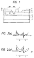
- this HEMT structure comprises an undoped semiconductor layer 2 disposed on a substrate 1; a doped semiconductor layer 3 whose electron affinity is smaller than that of the undoped semiconductor layer 2 and in which impurities are doped; a gate electrode 4 formed on the doped semiconductor layer 3; and a source electrode 6 and a drain electrode 7 which are respectively formed on a cap layer 5 at both sides of the gate electrode 4.
- the doped semiconductor layer 3 located immediately below the gate electrode is not completely depleted in a state in which the gate voltage is not applied, the two-dimensional electron gas accumulated in the heterojunction interface is directly controlled by the gate voltage which is under 0 volt.
- the source resistance is expressed by the sum of the contact resistance between the source electrode 6 and the cap layer 5 and the sheet resistance of the epitaxial growth layer.
- the sheet resistance of the epitaxial growth layer is further divided into portions (A) and (B), as shown in Fig. 1, and the resistance is particularly large in portion (B). The reason for this is that a plurality of current paths exist in portion (A), as shown at I1 and I2, and its resistance is therefore relatively small, whereas the number of paths is small in portion (B), as shown at I3.
- An energy band in a state in which the gate voltage is not applied and the doped semiconductor layer located immediately below the gate electrode is completely depleted is slightly high as a whole for both portion (B) and the portion located immediately below the gate electrode, as shown by the solid line in Fig. 5.
- practically no electrons remain in the doped semiconductor layer located immediately below the gate electrode and, likewise, practically no electrons remain in the doped semiconductor layer in portion (B).
- the energy band for portion (B) is not as high as at the portion located immediately below the gate electrode, but rises as shown by the dotted line in Fig. 5.
- the amount of electrons becomes small at portion (B) where the amount thereof is originally small. Accordingly, in a state of use, the electrons at portion (B) are not sufficient, and a resistance value becomes large, so that the noise is correspondingly large.
- the present invention has been made in view of these points, and has an object to provide a compound semiconductor device of a HEMT structure in which the resistance value at the aforementioned portion (B) is reduced, and a noise figure is thereby improved.
- a compound semiconductor device comprising: an undoped semiconductor layer; a doped semiconductor layer formed on the undoped semiconductor layer and having smaller electron affinity than the undoped semiconductor layer, impurities being doped in the doped semiconductor layer; a gate electrode formed on the doped semiconductor layer; and a source electrode and a drain electrode respectively formed at both sides of the gate electrode, wherein an impurity concentration of the doped semiconductor layer is selected such that a portion of the doped semiconductor layer located immediately below the gate electrode is not completely depleted in a state in which a gate voltage is not applied to the gate electrode, and is completely depleted in a state in which a negative voltage for minimizing a noise figure is applied to the gate electrode.
- an arrangement may be provided such that a planar doping region is provided in the vicinity of a center of the doped semiconductor layer, and impurities of the planar doping region located immediately below the gate electrode are not completely ionized in a state in which a gate voltage is not applied to the gate electrode, and are completely ionized in a state in which a negative voltage for minimizing a noise figure is applied to the gate electrode.
- the doped semiconductor layer located immediately below the gate electrode is not completely depleted in a state of non-application of a gate voltage, the amount of electrons in portion (B) is sufficiently large. Even if a negative voltage is applied to the gate, the amount of the electrons in portion (B) does not decrease substantially, so that the source-side resistance becomes small. Moreover, since the doped semiconductor layer located immediately below the gate electrode is completely depleted in the state in which the negative voltage is applied to the gate voltage, the essential operating characteristic of the HEMT is not impaired.
- the source-side resistance is lowered by the planar doping region provided in the doped semiconductor layer, in the same way as in the above-described first arrangement according to the first aspect.
- the structure of the compound semiconductor device itself is shown by a form similar to that of Fig. 1, but the first embodiment differs from the prior art in that the impurity concentration of the doped semiconductor layer is selected in such a manner as to satisfy the following conditions (1) and (2). That is,
- the amount of electrons is large at portion (B) in the state of non-application of the gate voltage. If the negative voltage is applied to the gate electrode, the energy band immediately below the gate rises on the whole from the solid line (the non-applied state) to the dotted line (the applied state), as shown in Fig. 2(b). However, the effect of the negative voltage applied to the gate is small at portion (B) in the doped semiconductor layer, and the energy band rises only slightly from the solid line (the non-applied state) to the dotted line (the applied state), as shown in Fig. 2(a). Accordingly, since a state of sufficient existence of electrons is held in this portion (B), in the state of use (in the state in which the negative voltage is applied to the gate), the resistance at portion (B) is substantially low as compared with the prior art.
- K is a fitting constant
- f a frequency
- fT a cutoff frequency
- gm the mutual conductance
- Rs the source resistance
- Rg the gate resistance
- the noise is reduced in the HEMT having a small source resistance Rs as in the above-described first embodiment.
- an undoped semiconductor layer 2 is formed of GaAs or InGaAs containing Ga at a ratio of 0.8.
- a doped semiconductor layer 3 is formed of n+AlGaAs (at a ratio of 0.22 of Al and 0.78 of Ga) doped with silicon having a concentration in the range of 2.5 x 10¹⁸/cm3 to 6 x 10¹⁸/cm3 as impurities.
- a cap layer 5 is constituted by n+GaAs.
- the undoped semiconductor layer 2, the doped semiconductor layer 3, and the cap layer 5 are formed consecutively on a substrate 1 through epitaxial growth.
- a planar doping region 9 is provided in the vicinity of the center of the doped semiconductor layer 3, as shown in Fig. 3.
- this planar doping region 9 all the impurities thereof are not ionized in the state in which the voltage is not applied to a gate electrode 4, whereas all of them are ionized when a negative voltage for minimizing the noise is applied to the gate electrode.
- the source resistance becomes small for a reason similar to that for the above-described first embodiment, thereby reducing the noise.
- Fig. 4 shows an energy band for a portion located immediately below the gate electrode shown in Fig. 3.
- the solid line is the case where the gate voltage is not applied, while the dotted line shows the case when the negative gate voltage is applied.
- the planar doping region 9 is a portion of the doped semiconductor layer 3 of AlGaAs (Al: 0.22, Ga: 0.8) doped with Si in the range of 5 x 10¹⁷/cm3 to 2.0 x 10¹⁸/cm3, in which Si in the range of 5 x 10¹¹/cm2 to 6 x 10¹²/cm2 is further doped.
- the other portions 2, 5 are formed of the same materials as those shown in Fig. 2.
- a compound semiconductor device includes an undoped semiconductor layer; a doped semiconductor layer formed on the undoped semiconductor layer and having smaller electron affinity than the undoped semiconductor layer, impurities being doped in the doped semiconductor layer; a gate electrode formed on the doped semiconductor layer; and a source electrode and a drain electrode respectively formed at both sides of the gate electrode, wherein an impurity concentration of the doped semiconductor layer is selected such that a portion of the doped semiconductor layer located immediately below the gate electrode is not completely depleted in a state in which a gate voltage is not applied to the gate electrode, and is completely depleted in a state in which a negative voltage for minimizing a noise figure is applied to the gate electrode.
Landscapes
- Junction Field-Effect Transistors (AREA)
- Insulated Gate Type Field-Effect Transistor (AREA)
Abstract
Description
- The present invention relates to a compound semiconductor device such as a HEMT (High Electron Mobility Transistor).
- A HEMT structure is attracting attention as a field-effect transistor making use of a two-dimensional electron gas accumulated in a heterojunction interface. As shown in Fig. 1, this HEMT structure comprises an
undoped semiconductor layer 2 disposed on asubstrate 1; adoped semiconductor layer 3 whose electron affinity is smaller than that of theundoped semiconductor layer 2 and in which impurities are doped; a gate electrode 4 formed on thedoped semiconductor layer 3; and asource electrode 6 and adrain electrode 7 which are respectively formed on acap layer 5 at both sides of the gate electrode 4. Though thedoped semiconductor layer 3 located immediately below the gate electrode is not completely depleted in a state in which the gate voltage is not applied, the two-dimensional electron gas accumulated in the heterojunction interface is directly controlled by the gate voltage which is under 0 volt. - However, with the conventional HEMT structure in which the doped semiconductor layer located immediately below the gate electrode is completely depleted in the state in which the gate voltage is not applied, the source resistance is large, and the noise characteristic in a high frequency is deteriorated. To explain this point, first, the source resistance is expressed by the sum of the contact resistance between the
source electrode 6 and thecap layer 5 and the sheet resistance of the epitaxial growth layer. As shown in Fig. 1, the sheet resistance of the epitaxial growth layer is further divided into portions (A) and (B), as shown in Fig. 1, and the resistance is particularly large in portion (B). The reason for this is that a plurality of current paths exist in portion (A), as shown at I1 and I2, and its resistance is therefore relatively small, whereas the number of paths is small in portion (B), as shown at I3. - An energy band in a state in which the gate voltage is not applied and the doped semiconductor layer located immediately below the gate electrode is completely depleted, is slightly high as a whole for both portion (B) and the portion located immediately below the gate electrode, as shown by the solid line in Fig. 5. As such, practically no electrons remain in the doped semiconductor layer located immediately below the gate electrode and, likewise, practically no electrons remain in the doped semiconductor layer in portion (B). Then, when a negative voltage is applied to the gate electrode, the energy band for portion (B) is not as high as at the portion located immediately below the gate electrode, but rises as shown by the dotted line in Fig. 5. For this reason, the amount of electrons becomes small at portion (B) where the amount thereof is originally small. Accordingly, in a state of use, the electrons at portion (B) are not sufficient, and a resistance value becomes large, so that the noise is correspondingly large.
- To lower the resistance at portion (B), it suffices to increase the amount of electrons by increasing the impurity concentration of the doped semiconductor layer, but if the concentration is made excessively high, the portion of the doped semiconductor layer located immediately below the gate does not become depleted when the gate voltage is applied. Hence, if the device is operated in that state, it is impossible to obtain a satisfactory characteristic.
- The present invention has been made in view of these points, and has an object to provide a compound semiconductor device of a HEMT structure in which the resistance value at the aforementioned portion (B) is reduced, and a noise figure is thereby improved.
- To attain the aforementioned object, according to a first aspect of the present invention, there is provided a compound semiconductor device comprising: an undoped semiconductor layer; a doped semiconductor layer formed on the undoped semiconductor layer and having smaller electron affinity than the undoped semiconductor layer, impurities being doped in the doped semiconductor layer; a gate electrode formed on the doped semiconductor layer; and a source electrode and a drain electrode respectively formed at both sides of the gate electrode, wherein an impurity concentration of the doped semiconductor layer is selected such that a portion of the doped semiconductor layer located immediately below the gate electrode is not completely depleted in a state in which a gate voltage is not applied to the gate electrode, and is completely depleted in a state in which a negative voltage for minimizing a noise figure is applied to the gate electrode.
- In addition, according to a second aspect of the present invention, an arrangement may be provided such that a planar doping region is provided in the vicinity of a center of the doped semiconductor layer, and impurities of the planar doping region located immediately below the gate electrode are not completely ionized in a state in which a gate voltage is not applied to the gate electrode, and are completely ionized in a state in which a negative voltage for minimizing a noise figure is applied to the gate electrode.
- In accordance with the above-described first aspect of the present invention, since the doped semiconductor layer located immediately below the gate electrode is not completely depleted in a state of non-application of a gate voltage, the amount of electrons in portion (B) is sufficiently large. Even if a negative voltage is applied to the gate, the amount of the electrons in portion (B) does not decrease substantially, so that the source-side resistance becomes small. Moreover, since the doped semiconductor layer located immediately below the gate electrode is completely depleted in the state in which the negative voltage is applied to the gate voltage, the essential operating characteristic of the HEMT is not impaired.
- In accordance with the above-described second aspect of the present invention, the source-side resistance is lowered by the planar doping region provided in the doped semiconductor layer, in the same way as in the above-described first arrangement according to the first aspect.
-
- Fig. 1 is a diagram of the structure of a compound semiconductor device of a HEMT structure to which the present invention is applied;
- Figs. 2(a) and 2(b) are energy band diagrams of the device according to the present invention;
- Fig. 3 is a diagram of the structure of a compound semiconductor device according to another embodiment of the present invention;
- Fig. 4 is an energy band diagram of the device shown in Fig. 3; and
- Fig. 5 is an energy band diagram of a conventional device.
- In a first embodiment of the present invention, the structure of the compound semiconductor device itself is shown by a form similar to that of Fig. 1, but the first embodiment differs from the prior art in that the impurity concentration of the doped semiconductor layer is selected in such a manner as to satisfy the following conditions (1) and (2). That is,
- (1) The doped semiconductor layer located immediately below the gate electrode is not completely depleted in the state in which the gate voltage is not applied to the gate electrode. In other words, in the doped semiconductor layer located immediately below the gate electrode, the sum of a depletion layer extending from the gate electrode side and a depletion layer extending from the undoped semiconductor layer side is smaller than the thickness of the doped semiconductor layer.
If this is shown in terms of an energy band, this means that, as shown by the solid line in Fig. 2(b), a portion in the vicinity of a Fermi level EF exists in the center of the doped semiconductor layer located immediately below the gate electrode. - (2) In a state in which a negative voltage for minimizing the noise figure is applied to the gate electrode, the doped semiconductor layer located immediately below the gate electrode is completely depleted (as shown by dotted line in Fig. 2(b)).
- If the above-described measure is taken, the amount of electrons is large at portion (B) in the state of non-application of the gate voltage. If the negative voltage is applied to the gate electrode, the energy band immediately below the gate rises on the whole from the solid line (the non-applied state) to the dotted line (the applied state), as shown in Fig. 2(b). However, the effect of the negative voltage applied to the gate is small at portion (B) in the doped semiconductor layer, and the energy band rises only slightly from the solid line (the non-applied state) to the dotted line (the applied state), as shown in Fig. 2(a). Accordingly, since a state of sufficient existence of electrons is held in this portion (B), in the state of use (in the state in which the negative voltage is applied to the gate), the resistance at portion (B) is substantially low as compared with the prior art.
- A noise figure NF is given by

In this formula, K is a fitting constant; f, a frequency; fT, a cutoff frequency; gm, the mutual conductance; Rs, the source resistance; and Rg, the gate resistance. - As can be seen from this formula, the noise is reduced in the HEMT having a small source resistance Rs as in the above-described first embodiment.
- In the above-described first embodiment, for instance, an
undoped semiconductor layer 2 is formed of GaAs or InGaAs containing Ga at a ratio of 0.8. Adoped semiconductor layer 3 is formed of n⁺AlGaAs (at a ratio of 0.22 of Al and 0.78 of Ga) doped with silicon having a concentration in the range of 2.5 x 10¹⁸/cm³ to 6 x 10¹⁸/cm³ as impurities. In addition, acap layer 5 is constituted by n⁺GaAs. - The
undoped semiconductor layer 2, thedoped semiconductor layer 3, and thecap layer 5 are formed consecutively on asubstrate 1 through epitaxial growth. - Next, in a second embodiment, a
planar doping region 9 is provided in the vicinity of the center of thedoped semiconductor layer 3, as shown in Fig. 3. In thisplanar doping region 9, all the impurities thereof are not ionized in the state in which the voltage is not applied to a gate electrode 4, whereas all of them are ionized when a negative voltage for minimizing the noise is applied to the gate electrode. In the case of the second embodiment thus constructed, the source resistance becomes small for a reason similar to that for the above-described first embodiment, thereby reducing the noise. Fig. 4 shows an energy band for a portion located immediately below the gate electrode shown in Fig. 3. Here, the solid line is the case where the gate voltage is not applied, while the dotted line shows the case when the negative gate voltage is applied. - In the embodiment shown in Fig. 3, the
planar doping region 9 is a portion of thedoped semiconductor layer 3 of AlGaAs (Al: 0.22, Ga: 0.8) doped with Si in the range of 5 x 10¹⁷/cm³ to 2.0 x 10¹⁸/cm³, in which Si in the range of 5 x 10¹¹/cm² to 6 x 10¹²/cm² is further doped. Theother portions - As described above, in accordance with the compound semiconductor device of the present invention, advantages are obtained in that the source resistance becomes small, and that the noise figure is improved.
- A compound semiconductor device includes an undoped semiconductor layer; a doped semiconductor layer formed on the undoped semiconductor layer and having smaller electron affinity than the undoped semiconductor layer, impurities being doped in the doped semiconductor layer; a gate electrode formed on the doped semiconductor layer; and a source electrode and a drain electrode respectively formed at both sides of the gate electrode, wherein an impurity concentration of the doped semiconductor layer is selected such that a portion of the doped semiconductor layer located immediately below the gate electrode is not completely depleted in a state in which a gate voltage is not applied to the gate electrode, and is completely depleted in a state in which a negative voltage for minimizing a noise figure is applied to the gate electrode.
Claims (6)
- A compound semiconductor device comprising: an undoped semiconductor layer; a doped semiconductor layer formed on said undoped semiconductor layer and having smaller electron affinity than said undoped semiconductor layer, impurities being doped in said doped semiconductor layer; a gate electrode formed on said doped semiconductor layer; and a source electrode and a drain electrode respectively formed at both sides of said gate electrode,
wherein an impurity concentration of said doped semiconductor layer is selected such that a portion of said doped semiconductor layer located immediately below said gate electrode is not completely depleted in a state in which a gate voltage is not applied to said gate electrode, and is completely depleted in a state in which a negative voltage for minimizing a noise figure is applied to said gate electrode. - A compound semiconductor device as claimed in claim 1, wherein said impurity concentration of said doped semiconductor layer is 2.5 x 10¹⁸/cm³ or more.
- A compound semiconductor device comprising: an undoped semiconductor layer; a doped semiconductor layer formed on said undoped semiconductor layer and having smaller electron affinity than said undoped semiconductor layer, impurities being doped in said doped semiconductor layer; a gate electrode formed on said doped semiconductor layer; and a source electrode and a drain electrode respectively formed at both sides of said gate electrode,
wherein a planar doping region is provided in the vicinity of a center of said doped semiconductor layer, and impurities of said planar doping region located immediately below said gate electrode are not completely ionized in a state in which a gate voltage is not applied to said gate electrode, and are completely ionized in a state in which a negative voltage for minimizing a noise figure is applied to said gate electrode. - A compound semiconductor device as claimed in claim 3, wherein an impurity concentration of said doped semiconductor layer is 2.0 x 10¹⁸/cm³ or less and impurities of 5 x 10¹¹/cm² or more is further doped in said planar doping region.
- A compound semiconductor device as claimed in claim 2, wherein said impurity concentration of said doped semiconductor layer is 6 x 10¹⁸/cm³ or less.
- A compound semiconductor device as claimed in claim 4, wherein said impurity concentration of said doped semiconductor layer is 5 x 10¹⁷/cm³ or more, and said impurities of 6 x 10¹²/cm² or less is further doped in said planar doping region.
Applications Claiming Priority (2)
| Application Number | Priority Date | Filing Date | Title |
|---|---|---|---|
| JP3311827A JPH05121454A (en) | 1991-10-29 | 1991-10-29 | Compound semiconductor device |
| JP311827/91 | 1991-10-29 |
Publications (3)
| Publication Number | Publication Date |
|---|---|
| EP0539690A2 true EP0539690A2 (en) | 1993-05-05 |
| EP0539690A3 EP0539690A3 (en) | 1994-02-02 |
| EP0539690B1 EP0539690B1 (en) | 1997-02-05 |
Family
ID=18021880
Family Applications (1)
| Application Number | Title | Priority Date | Filing Date |
|---|---|---|---|
| EP92114718A Expired - Lifetime EP0539690B1 (en) | 1991-10-29 | 1992-08-28 | Compound semiconductor device |
Country Status (5)
| Country | Link |
|---|---|
| US (1) | US5343056A (en) |
| EP (1) | EP0539690B1 (en) |
| JP (1) | JPH05121454A (en) |
| CA (1) | CA2078941C (en) |
| DE (1) | DE69217326T2 (en) |
Families Citing this family (1)
| Publication number | Priority date | Publication date | Assignee | Title |
|---|---|---|---|---|
| JP3123940B2 (en) * | 1997-03-27 | 2001-01-15 | 日本電気株式会社 | Field effect transistor and method of manufacturing the same |
Family Cites Families (3)
| Publication number | Priority date | Publication date | Assignee | Title |
|---|---|---|---|---|
| JPS5728322A (en) * | 1980-07-28 | 1982-02-16 | Fujitsu Ltd | Formation of semiconductor single crystal layer |
| JPS62266874A (en) * | 1986-05-15 | 1987-11-19 | Fujitsu Ltd | Semiconductor device |
| JPH01171279A (en) * | 1987-12-25 | 1989-07-06 | Mitsubishi Monsanto Chem Co | Semiconductor device |
-
1991
- 1991-10-29 JP JP3311827A patent/JPH05121454A/en active Pending
-
1992
- 1992-08-17 US US07/931,042 patent/US5343056A/en not_active Expired - Fee Related
- 1992-08-28 DE DE69217326T patent/DE69217326T2/en not_active Expired - Fee Related
- 1992-08-28 EP EP92114718A patent/EP0539690B1/en not_active Expired - Lifetime
- 1992-09-23 CA CA002078941A patent/CA2078941C/en not_active Expired - Fee Related
Non-Patent Citations (7)
| Title |
|---|
| APPLIED PHYSICS LETTERS vol. 49, no. 25 , 22 December 1986 , NEW YORK US pages 1729 - 1731 E. F. SCHUBERT ET AL. 'SELF-ALIGNED ENHANCEMENT-MODE AND DEPLETION-MODE GaAs FIELD-EFFECT TRANSISTORS EMPLOYING THE DELTA-DOPING TECHNIQUE' * |
| IEEE ED-28,7, pp. 790-795 * |
| IEEE ED-29,5, pp. 955-960 * |
| IEEE MILITARY COMMUNICATIONS CONFERENCE October 1989 , BOSTON, MASSACHUSETTS, USA pages 735 - 738 XP131906 E. D. ARCHER ET AL. 'KA/Q-BAND BROADBAND, KA AND W-BAND LOW NOISE HEMT AMPLIFIERS' * |
| IEEE TRANSACTIONS ON MICROWAVE THEORY AND TECHNIQUES vol. 36, no. 7 , July 1988 , NEW YORK US pages 1124 - 1140 XP118143 G. SALMER ET AL. 'MODELING OF MODFET'S' * |
| JOURNAL OF VACUUM SCIENCE AND TECHNOLOGY B vol. 2 , April 1984 , NEW YORK, USA pages 113 - 116 K. LEE ET AL. 'CHARGE CONTROL MODEL OF INVERTED GaAs-AlGaAs MODULATION DOPED FET'S (IMODFET'S)' * |
| PHYSICA B+C vol. 117-118 , 1983 , AMSTERDAM, NORTH-HOLLAND pages 756 - 758 R. H. WALLIS 'EFFECT OF FREE CARRIER SCREENING ON THE ELECTRON MOBILITY OF GaAs : A STUDY BY FIELD-EFFECT MEASUREMENTS' * |
Also Published As
| Publication number | Publication date |
|---|---|
| DE69217326D1 (en) | 1997-03-20 |
| DE69217326T2 (en) | 1997-08-07 |
| EP0539690B1 (en) | 1997-02-05 |
| US5343056A (en) | 1994-08-30 |
| EP0539690A3 (en) | 1994-02-02 |
| JPH05121454A (en) | 1993-05-18 |
| CA2078941C (en) | 1997-01-21 |
| CA2078941A1 (en) | 1993-04-30 |
Similar Documents
| Publication | Publication Date | Title |
|---|---|---|
| US20230207636A1 (en) | High Voltage Blocking III-V Semiconductor Device | |
| US6548333B2 (en) | Aluminum gallium nitride/gallium nitride high electron mobility transistors having a gate contact on a gallium nitride based cap segment | |
| US11769825B2 (en) | Nitride semiconductor device and nitride semiconductor package | |
| US5105241A (en) | Field effect transistor | |
| US5319223A (en) | High electron mobility transistor | |
| US4605945A (en) | Semiconductor device | |
| EP0482726A2 (en) | Heterojunction field-effect transistor | |
| US5650642A (en) | Field effect semiconductor device | |
| US4980731A (en) | Atomic planar-doped field-effect transistor | |
| EP0539693A2 (en) | Compound semiconductor device | |
| US5847414A (en) | Semiconductor device having a hetero-junction between SiC and a Group 3B-nitride | |
| JP3483716B2 (en) | Semiconductor device | |
| EP0602671B1 (en) | Heterojunction field effect transistor having an improved transistor characteristic | |
| EP0539690A2 (en) | Compound semiconductor device | |
| US5751027A (en) | Field effect semiconductor device with a low-noise drift layer and a high-power drift layer | |
| US5159414A (en) | Junction field effect transistor of a compound semiconductor | |
| EP0314877A1 (en) | Power high election mobility structure | |
| EP0271080B1 (en) | Indium-phosphide hetero-mis-gate field effect transistor | |
| EP0558011A2 (en) | High electron mobility transistor | |
| KR950006493B1 (en) | High-low dopping algoas/gaas hemt device | |
| JPS5891681A (en) | field effect transistor | |
| JPH0513462A (en) | Compound semiconductor structure | |
| JPH04365333A (en) | Hetero junction field effect transistor and its manufacture | |
| JPH0729917A (en) | Field effect transistor and method of manufacturing the same | |
| JPH0547799A (en) | Semiconductor device |
Legal Events
| Date | Code | Title | Description |
|---|---|---|---|
| PUAI | Public reference made under article 153(3) epc to a published international application that has entered the european phase |
Free format text: ORIGINAL CODE: 0009012 |
|
| AK | Designated contracting states |
Kind code of ref document: A2 Designated state(s): DE FR GB |
|
| PUAL | Search report despatched |
Free format text: ORIGINAL CODE: 0009013 |
|
| AK | Designated contracting states |
Kind code of ref document: A3 Designated state(s): DE FR GB |
|
| 17P | Request for examination filed |
Effective date: 19940208 |
|
| 17Q | First examination report despatched |
Effective date: 19950530 |
|
| GRAG | Despatch of communication of intention to grant |
Free format text: ORIGINAL CODE: EPIDOS AGRA |
|
| GRAH | Despatch of communication of intention to grant a patent |
Free format text: ORIGINAL CODE: EPIDOS IGRA |
|
| GRAH | Despatch of communication of intention to grant a patent |
Free format text: ORIGINAL CODE: EPIDOS IGRA |
|
| GRAA | (expected) grant |
Free format text: ORIGINAL CODE: 0009210 |
|
| AK | Designated contracting states |
Kind code of ref document: B1 Designated state(s): DE FR GB |
|
| REF | Corresponds to: |
Ref document number: 69217326 Country of ref document: DE Date of ref document: 19970320 |
|
| ET | Fr: translation filed | ||
| PLBE | No opposition filed within time limit |
Free format text: ORIGINAL CODE: 0009261 |
|
| 26N | No opposition filed | ||
| PGFP | Annual fee paid to national office [announced via postgrant information from national office to epo] |
Ref country code: FR Payment date: 20010810 Year of fee payment: 10 |
|
| PGFP | Annual fee paid to national office [announced via postgrant information from national office to epo] |
Ref country code: DE Payment date: 20010820 Year of fee payment: 10 |
|
| PGFP | Annual fee paid to national office [announced via postgrant information from national office to epo] |
Ref country code: GB Payment date: 20010822 Year of fee payment: 10 |
|
| REG | Reference to a national code |
Ref country code: GB Ref legal event code: IF02 |
|
| PG25 | Lapsed in a contracting state [announced via postgrant information from national office to epo] |
Ref country code: GB Free format text: LAPSE BECAUSE OF NON-PAYMENT OF DUE FEES Effective date: 20020828 |
|
| PG25 | Lapsed in a contracting state [announced via postgrant information from national office to epo] |
Ref country code: DE Free format text: LAPSE BECAUSE OF NON-PAYMENT OF DUE FEES Effective date: 20030301 |
|
| GBPC | Gb: european patent ceased through non-payment of renewal fee |
Effective date: 20020828 |
|
| PG25 | Lapsed in a contracting state [announced via postgrant information from national office to epo] |
Ref country code: FR Free format text: LAPSE BECAUSE OF NON-PAYMENT OF DUE FEES Effective date: 20030430 |
|
| REG | Reference to a national code |
Ref country code: FR Ref legal event code: ST |