EP0538813B1 - Optical head for an authenticity identifying system - Google Patents
Optical head for an authenticity identifying system Download PDFInfo
- Publication number
- EP0538813B1 EP0538813B1 EP92117982A EP92117982A EP0538813B1 EP 0538813 B1 EP0538813 B1 EP 0538813B1 EP 92117982 A EP92117982 A EP 92117982A EP 92117982 A EP92117982 A EP 92117982A EP 0538813 B1 EP0538813 B1 EP 0538813B1
- Authority
- EP
- European Patent Office
- Prior art keywords
- optical head
- light
- light emitting
- photodiodes
- emitting element
- Prior art date
- Legal status (The legal status is an assumption and is not a legal conclusion. Google has not performed a legal analysis and makes no representation as to the accuracy of the status listed.)
- Expired - Lifetime
Links
Images
Classifications
-
- G—PHYSICS
- G06—COMPUTING OR CALCULATING; COUNTING
- G06K—GRAPHICAL DATA READING; PRESENTATION OF DATA; RECORD CARRIERS; HANDLING RECORD CARRIERS
- G06K7/00—Methods or arrangements for sensing record carriers, e.g. for reading patterns
- G06K7/10—Methods or arrangements for sensing record carriers, e.g. for reading patterns by electromagnetic radiation, e.g. optical sensing; by corpuscular radiation
- G06K7/10544—Methods or arrangements for sensing record carriers, e.g. for reading patterns by electromagnetic radiation, e.g. optical sensing; by corpuscular radiation by scanning of the records by radiation in the optical part of the electromagnetic spectrum
- G06K7/10821—Methods or arrangements for sensing record carriers, e.g. for reading patterns by electromagnetic radiation, e.g. optical sensing; by corpuscular radiation by scanning of the records by radiation in the optical part of the electromagnetic spectrum further details of bar or optical code scanning devices
- G06K7/10841—Particularities of the light-sensitive elements
-
- G—PHYSICS
- G03—PHOTOGRAPHY; CINEMATOGRAPHY; ANALOGOUS TECHNIQUES USING WAVES OTHER THAN OPTICAL WAVES; ELECTROGRAPHY; HOLOGRAPHY
- G03H—HOLOGRAPHIC PROCESSES OR APPARATUS
- G03H1/00—Holographic processes or apparatus using light, infrared or ultraviolet waves for obtaining holograms or for obtaining an image from them; Details peculiar thereto
- G03H1/26—Processes or apparatus specially adapted to produce multiple sub- holograms or to obtain images from them, e.g. multicolour technique
- G03H1/30—Processes or apparatus specially adapted to produce multiple sub- holograms or to obtain images from them, e.g. multicolour technique discrete holograms only
-
- G—PHYSICS
- G06—COMPUTING OR CALCULATING; COUNTING
- G06K—GRAPHICAL DATA READING; PRESENTATION OF DATA; RECORD CARRIERS; HANDLING RECORD CARRIERS
- G06K19/00—Record carriers for use with machines and with at least a part designed to carry digital markings
- G06K19/06—Record carriers for use with machines and with at least a part designed to carry digital markings characterised by the kind of the digital marking, e.g. shape, nature, code
- G06K19/08—Record carriers for use with machines and with at least a part designed to carry digital markings characterised by the kind of the digital marking, e.g. shape, nature, code using markings of different kinds or more than one marking of the same kind in the same record carrier, e.g. one marking being sensed by optical and the other by magnetic means
- G06K19/10—Record carriers for use with machines and with at least a part designed to carry digital markings characterised by the kind of the digital marking, e.g. shape, nature, code using markings of different kinds or more than one marking of the same kind in the same record carrier, e.g. one marking being sensed by optical and the other by magnetic means at least one kind of marking being used for authentication, e.g. of credit or identity cards
- G06K19/16—Record carriers for use with machines and with at least a part designed to carry digital markings characterised by the kind of the digital marking, e.g. shape, nature, code using markings of different kinds or more than one marking of the same kind in the same record carrier, e.g. one marking being sensed by optical and the other by magnetic means at least one kind of marking being used for authentication, e.g. of credit or identity cards the marking being a hologram or diffraction grating
Definitions
- the present invention relates to a system for determining or identifying the authenticity of such articles as information storage cards by means of a reader/writer to prevent unauthorized fabrication and alteration of such articles or cards, and in particular to an optical head which is suitable for use in such a system.
- the information storage cards include, not exclusively, magnetic cards, IC cards, optical cards and so on which are capable of exchanging information with reader/writers.
- DE-A-24 44 961 discloses a character recognition system which employs an optical head having a plurality of light receiving sectors arranged concentrically.
- the light emitting element is not shown in the drawings. It simply and generally illuminates the document to be read. Further, the said document suggests the use of a single wafer including an array of photo-diodes. It does, however, not suggest any opening in the wafer for defining an aperture for the light emitting element. Also, the said document does not suggest the use of a hologram.
- a further object is to provide such an optical head which is economical to manufacture.
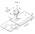
- Figure 1 shows a card reader/writer to which a preferred embodiment of the present invention is applied.
- the card 1 is conveyed in the direction indicated by the arrows or substantially laterally as seen in Figure 1 by means of conveyer rollers or the like not shown in the drawing, and a magnetic head 3 writes into and reads out of a magnetic stripe 2 provided on a major surface 1a of the card 1 when it has reached such a position.
- a holograph region 4 is provided on a suitable location of the major surface 1a of the card 1.
- This holograph region 4 consists of a reflective holograph having such a reflective property that incident light having a certain wave length and projected perpendicularly upon the holograph is reflected in a certain prescribed direction or certain prescribed directions.
- the identification region may consist of a holograph, a diffraction grating or a multiplicity of parallel grooves.
- the reader/writer is provided with an optical head 5 according to the present invention for projecting a coherent beam of laser light perpendicularly upon the major surface 1a of the card 1, in particular upon the holograph region 4, and receiving the light reflected therefrom as described hereinafter.
- An identification circuit 19 is connected to the optical head 5 to determine the authenticity of each card.
- the card 1 inserted in the card reader/writer is retained perpendicularly to the illuminating light beam from the optical head 5, and the illuminating light or the incident light from the optical head 5 is projected upon the holograph region 4.
- the authenticity of the card 1 can be identified when the light reflected by the holograph region 4 is collected by the optical head 5 in a certain pattern, and its intensity is detected to be of a certain level by the identification circuit 19. Therefore, even when a forger obtained such a card, not only it would be difficult for him to analyze and duplicate the holograph but also a significant cost is required to fabricate an identical holograph. Thereby, it offers a strong discouraging effect upon potential forgers.
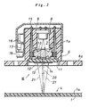
- FIGs 2 and 3 show the preferred embodiment of the optical head according to the present invention.
- This optical head 5 comprises an annular casing 6 made of synthetic resin and provided with a flange 6a at a bottom end thereof, a light emitting element 8 consisting of a semiconductor laser device at a top end of a central bore 7 defined in the casing 6, and a lens 8 fixedly fitted into an enlarged part 7a of the central bore 7 in a lower part thereof.
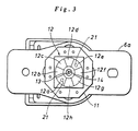
- the bottom end (the lower end as seen in Figure 2) of the central bore 7 is closed by a circuit board 11 having an octagonal shape as illustrated in Figure 3.
- a semiconductor chip 12 consisting of a silicon chip is mounted on the bottom surface of the circuit board 11.
- the circuit board 11 is provided with a central opening 13 for allowing a coherent light beam emitted from the light emitting element 8 and collimated by the lens 10 to pass through.
- the central opening 13 of the circuit board 11 serves as a diaphragm which limits the aperture of the lens 10.
- the semiconductor chip 12 is divided into eight sectors 12a through 12h of an equal size, and is provided with a central opening 14 which is coaxial with the opening 13 of the circuit board 11 and is larger in diameter than the opening 13.
- Each of the sectors 12a through 12h is formed as an individual photodiode.
- the identification of the identification region can be accomplished by detecting the pattern of light received by these sectors.
- the opening 13 or the central aperture serves as a diaphragm.
- a flexible circuit board 9 is attached to an axial upper end surface of the casing 6 remote from the flange 6a, and a part of the flexible circuit board 9 extends along a side of the casing 6. Pins 15 connected to the sectors 12a through 12h of the semiconductor chip 12 along with pins extending from the light emitting element 8 are soldered to appropriate parts of the flexible circuit board 9.
- the flexible circuit board 9 carries various circuit elements 16, and lead wires 18 are connected to appropriate parts of the circuit formed on the flexible circuit board 9 via a connector 17.
- the light receiving surface may be simply divided into a plurality of sectors 12a through 12h arranged around the central opening 14 as illustrated in Figure 3, or, alternatively, may be divided into two or more rows of sectors arranged around the central opening 14.
Landscapes
- Physics & Mathematics (AREA)
- Engineering & Computer Science (AREA)
- General Physics & Mathematics (AREA)
- Theoretical Computer Science (AREA)
- Electromagnetism (AREA)
- General Health & Medical Sciences (AREA)
- Toxicology (AREA)
- Health & Medical Sciences (AREA)
- Artificial Intelligence (AREA)
- Computer Vision & Pattern Recognition (AREA)
- Optical Head (AREA)
- Credit Cards Or The Like (AREA)
- Holo Graphy (AREA)
Description
- The present invention relates to a system for determining or identifying the authenticity of such articles as information storage cards by means of a reader/writer to prevent unauthorized fabrication and alteration of such articles or cards, and in particular to an optical head which is suitable for use in such a system. The information storage cards include, not exclusively, magnetic cards, IC cards, optical cards and so on which are capable of exchanging information with reader/writers.
- Conventionally, to the end of preventing the forgery of, for instance, a magnetic card, it has been practiced to use a laminated structure for its magnetic layer, and to punch holes in the magnetic card when the magnetic card is not intended for repeated use. However, such structures can be duplicated with deceitful intention by the forgers with relative ease, and may not be sufficient to discourage attempts to illegally duplicate and alter the card. The internal structure of the card may be made more complex by known means, but it will lead to the complication and cost increase of the reader/writers for reading and writing information into and out of the card. A holograph or other optically conditioned region having a prescribed directivity may be used for identification purpose, but the system for optically identifying it tends to be complex, expensive and large in size.
- DE-A-24 44 961 discloses a character recognition system which employs an optical head having a plurality of light receiving sectors arranged concentrically. The light emitting element is not shown in the drawings. It simply and generally illuminates the document to be read. Further, the said document suggests the use of a single wafer including an array of photo-diodes. It does, however, not suggest any opening in the wafer for defining an aperture for the light emitting element. Also, the said document does not suggest the use of a hologram.
- It is the object of the invention to provide an optical head for optically determining authenticity of an article by impinging a light beam upon an identification region provided on the article and having a selected reflective directivity, and receiving light reflected by the identification region, which is highly compact in structure.
- A further object is to provide such an optical head which is economical to manufacture.
- These and other objects of the present invention can be accomplished by the teaching of claim 1.
- Now the present invention is described in the following with reference to the appended drawings, in which:
- Figure 1 is a perspective view of a card and an essential part of a card reader/writer to which the present invention is applied;
- Figures 2 is a sectional view of the optical head according to the present invention taken along line II-II of Figure 1; and
- Figure 3 is a bottom view of the optical head as seen in the direction indicated by III in Figure 2.
-
- Figure 1 shows a card reader/writer to which a preferred embodiment of the present invention is applied. The card 1 is conveyed in the direction indicated by the arrows or substantially laterally as seen in Figure 1 by means of conveyer rollers or the like not shown in the drawing, and a
magnetic head 3 writes into and reads out of a magnetic stripe 2 provided on amajor surface 1a of the card 1 when it has reached such a position. - A holograph region 4 is provided on a suitable location of the
major surface 1a of the card 1. This holograph region 4 consists of a reflective holograph having such a reflective property that incident light having a certain wave length and projected perpendicularly upon the holograph is reflected in a certain prescribed direction or certain prescribed directions. The identification region may consist of a holograph, a diffraction grating or a multiplicity of parallel grooves. - The reader/writer is provided with an
optical head 5 according to the present invention for projecting a coherent beam of laser light perpendicularly upon themajor surface 1a of the card 1, in particular upon the holograph region 4, and receiving the light reflected therefrom as described hereinafter. Anidentification circuit 19 is connected to theoptical head 5 to determine the authenticity of each card. - In carrying out such a card identification process, the card 1 inserted in the card reader/writer is retained perpendicularly to the illuminating light beam from the
optical head 5, and the illuminating light or the incident light from theoptical head 5 is projected upon the holograph region 4. The authenticity of the card 1 can be identified when the light reflected by the holograph region 4 is collected by theoptical head 5 in a certain pattern, and its intensity is detected to be of a certain level by theidentification circuit 19. Therefore, even when a forger obtained such a card, not only it would be difficult for him to analyze and duplicate the holograph but also a significant cost is required to fabricate an identical holograph. Thereby, it offers a strong discouraging effect upon potential forgers. - Figures 2 and 3 show the preferred embodiment of the optical head according to the present invention. This
optical head 5 comprises anannular casing 6 made of synthetic resin and provided with aflange 6a at a bottom end thereof, alight emitting element 8 consisting of a semiconductor laser device at a top end of acentral bore 7 defined in thecasing 6, and alens 8 fixedly fitted into an enlargedpart 7a of thecentral bore 7 in a lower part thereof. - The bottom end (the lower end as seen in Figure 2) of the
central bore 7 is closed by acircuit board 11 having an octagonal shape as illustrated in Figure 3. Asemiconductor chip 12 consisting of a silicon chip is mounted on the bottom surface of thecircuit board 11. Thecircuit board 11 is provided with acentral opening 13 for allowing a coherent light beam emitted from thelight emitting element 8 and collimated by thelens 10 to pass through. Thecentral opening 13 of thecircuit board 11 serves as a diaphragm which limits the aperture of thelens 10. - The
semiconductor chip 12 is divided into eightsectors 12a through 12h of an equal size, and is provided with acentral opening 14 which is coaxial with the opening 13 of thecircuit board 11 and is larger in diameter than the opening 13. Each of thesectors 12a through 12h is formed as an individual photodiode. The identification of the identification region can be accomplished by detecting the pattern of light received by these sectors. The opening 13 or the central aperture serves as a diaphragm. - A
flexible circuit board 9 is attached to an axial upper end surface of thecasing 6 remote from theflange 6a, and a part of theflexible circuit board 9 extends along a side of thecasing 6.Pins 15 connected to thesectors 12a through 12h of thesemiconductor chip 12 along with pins extending from thelight emitting element 8 are soldered to appropriate parts of theflexible circuit board 9. Theflexible circuit board 9 carriesvarious circuit elements 16, andlead wires 18 are connected to appropriate parts of the circuit formed on theflexible circuit board 9 via aconnector 17. - According to the present invention, the light receiving surface may be simply divided into a plurality of
sectors 12a through 12h arranged around thecentral opening 14 as illustrated in Figure 3, or, alternatively, may be divided into two or more rows of sectors arranged around thecentral opening 14.
Claims (8)
- An optical head (5) for optically determining the authenticity of an article (1) by impinging a light beam upon an identification region (4) provided on said article (1) and having a selected reflective directivity, and receiving light reflected by said identification region, comprising:characterized in thata light emitting element (8) for providing a coherent beam of lighta generally planar mounting means (11);a generally planar array of photodiodes (12) mounted on said mounting means (11) whereby said photodiodes do not receive direct light from said light emitting element, said array of photodiodes (12) being arranged around an axial centre line of said coherent light beam, each of said photodiodes (12a -12h) being adapted to individually detect a magnitude of light reflected from said identification region (4) of said article(1) and impinged thereon,the optical head further comprises an annular casing (6) defining a central bore (7) therein;said light emitting element is received coaxially at one end of said central bore (7) with a light emitting surface thereof facing interior of said central bore;said mounting means (11) is provided at an other end of said central bore (7) remote from said one end and includes an opening (13), disposed in a light path of said coherent light beam for allowing said coherent light beam to pass there through;said generally planar array of photodiodes is mounted on a surface of said mounting means facing away from said light emitting element (8) and is arranged around said opening (13).
- An optical head according to claim 1, wherein said planar array of photodiodes consists of a concentric array of photodiodes each having a sector-shaped light receiving surface.
- An optical head according to claim 2, wherein said sector-shaped light receiving surfaces are arranged in two rows around said aperture.
- An optical head according to claim 1, further comprising a circuit board (9) attached to said one end of said annular casing, said light emitting elements being mounted on said circuit board via leads of said light emitting element, said light receiving elements being provided with leads (15) which are passed through the annular casing and electrically and mechanical connected to said circuit board.
- An optical head according to claim 4, wherein said circuit board consists of a flexible circuit board, and is provided with an extension extending along a side of said annular casing and carrying at least one circuit element (16) for said light emitting element or said light receiving element.
- An optical head according to claim 1, wherein said array of photodiodes consisting of a single wafer having a central opening (14) passed through said wafer, and said sectors defined around said central opening.
- An optical head according to claim 1, wherein said light emitting element consists of a semiconductor laser device.
- An optical head according to claim 1, wherein said identification region consists of a holograph, a diffraction grating or a multiplicity of parallel grooves.
Applications Claiming Priority (2)
| Application Number | Priority Date | Filing Date | Title |
|---|---|---|---|
| US782976 | 1991-10-24 | ||
| US07/782,976 US5200794A (en) | 1989-08-11 | 1991-10-24 | Optical head for an optical authenticity identifing system |
Publications (3)
| Publication Number | Publication Date |
|---|---|
| EP0538813A2 EP0538813A2 (en) | 1993-04-28 |
| EP0538813A3 EP0538813A3 (en) | 1993-12-15 |
| EP0538813B1 true EP0538813B1 (en) | 2005-06-08 |
Family
ID=25127787
Family Applications (1)
| Application Number | Title | Priority Date | Filing Date |
|---|---|---|---|
| EP92117982A Expired - Lifetime EP0538813B1 (en) | 1991-10-24 | 1992-10-21 | Optical head for an authenticity identifying system |
Country Status (4)
| Country | Link |
|---|---|
| US (1) | US5200794A (en) |
| EP (1) | EP0538813B1 (en) |
| JP (1) | JPH0782513B2 (en) |
| DE (1) | DE69233521T2 (en) |
Families Citing this family (41)
| Publication number | Priority date | Publication date | Assignee | Title |
|---|---|---|---|---|
| US5442433A (en) * | 1989-08-11 | 1995-08-15 | Nhk Spring Co., Ltd. | Identification system for an article having individually attached patches |
| JPH05307633A (en) * | 1992-04-28 | 1993-11-19 | Nhk Spring Co Ltd | Identification structure for object and its identifying method |
| US5379131A (en) * | 1991-12-11 | 1995-01-03 | Dai Nippon Printing Co., Ltd. | Method of preventing forgery of diffraction grating pattern and forgery-proof diffraction grating pattern recording structure |
| WO1993012506A1 (en) * | 1991-12-19 | 1993-06-24 | Control Module Inc. | Secure optomagnetic identification |
| US5535023A (en) * | 1991-12-20 | 1996-07-09 | Dai Nippon Printing Co., Ltd. | Method of reading hologram information |
| JPH0797388B2 (en) * | 1992-09-29 | 1995-10-18 | 日本発条株式会社 | Object identification structure |
| JPH07210071A (en) * | 1994-01-25 | 1995-08-11 | Nhk Spring Co Ltd | Discrimination system for object |
| IL119562A (en) | 1996-11-04 | 2003-12-10 | Oridion Medical Ltd | Fluid analyzer with tube connector verifier |
| CH693693A5 (en) | 1997-06-06 | 2003-12-15 | Ovd Kinegram Ag | An apparatus for detecting optical diffraction markings. |
| EP0911758B1 (en) * | 1997-07-29 | 2005-11-30 | Nhk Spring Co.Ltd. | Optical identification system using cholesteric liquid crystals |
| CN1153099C (en) * | 1998-08-27 | 2004-06-09 | 日石三菱株式会社 | Genuine identification system and method for using genuine identification film |
| US6351537B1 (en) | 1998-10-05 | 2002-02-26 | 3M Innovative Properties Company | Verifiable holographic article |
| DE19924385A1 (en) | 1999-05-27 | 2000-12-07 | Xetos Ag | Information carrier with hologram |
| US7872804B2 (en) * | 2002-08-20 | 2011-01-18 | Illumina, Inc. | Encoded particle having a grating with variations in the refractive index |
| US7164533B2 (en) * | 2003-01-22 | 2007-01-16 | Cyvera Corporation | Hybrid random bead/chip based microarray |
| EP1535241A1 (en) * | 2002-08-20 | 2005-06-01 | Cyvera Corporation | Diffraction grating-based optical identification element |
| US7619819B2 (en) | 2002-08-20 | 2009-11-17 | Illumina, Inc. | Method and apparatus for drug product tracking using encoded optical identification elements |
| US20050227252A1 (en) * | 2002-08-20 | 2005-10-13 | Moon John A | Diffraction grating-based encoded articles for multiplexed experiments |
| US7900836B2 (en) | 2002-08-20 | 2011-03-08 | Illumina, Inc. | Optical reader system for substrates having an optically readable code |
| JP4485949B2 (en) * | 2002-08-20 | 2010-06-23 | シヴェラ コーポレイション | Grating-based coded microparticles for multiplex experiments |
| US7508608B2 (en) * | 2004-11-17 | 2009-03-24 | Illumina, Inc. | Lithographically fabricated holographic optical identification element |
| US7901630B2 (en) | 2002-08-20 | 2011-03-08 | Illumina, Inc. | Diffraction grating-based encoded microparticle assay stick |
| US7441703B2 (en) * | 2002-08-20 | 2008-10-28 | Illumina, Inc. | Optical reader for diffraction grating-based encoded optical identification elements |
| US7923260B2 (en) | 2002-08-20 | 2011-04-12 | Illumina, Inc. | Method of reading encoded particles |
| US20100255603A9 (en) | 2002-09-12 | 2010-10-07 | Putnam Martin A | Method and apparatus for aligning microbeads in order to interrogate the same |
| AU2003274979A1 (en) * | 2002-09-12 | 2004-04-30 | Cyvera Corporation | Chemical synthesis using diffraction grating-based encoded optical elements |
| US7092160B2 (en) | 2002-09-12 | 2006-08-15 | Illumina, Inc. | Method of manufacturing of diffraction grating-based optical identification element |
| AU2003267192A1 (en) * | 2002-09-12 | 2004-04-30 | Cyvera Corporation | Method and apparatus for aligning elongated microbeads in order to interrogate the same |
| EP1540591A1 (en) * | 2002-09-12 | 2005-06-15 | Cyvera Corporation | Diffraction grating-based encoded micro-particles for multiplexed experiments |
| CA2499037A1 (en) * | 2002-09-12 | 2004-03-25 | Cyvera Corporation | Method and apparatus for labelling using diffraction grating-based encoded optical identification elements |
| AU2003270655A1 (en) * | 2002-09-12 | 2004-04-30 | Cyvera Corporation | Assay stick comprising coded microbeads |
| US20060057729A1 (en) * | 2003-09-12 | 2006-03-16 | Illumina, Inc. | Diffraction grating-based encoded element having a substance disposed thereon |
| US7433123B2 (en) | 2004-02-19 | 2008-10-07 | Illumina, Inc. | Optical identification element having non-waveguide photosensitive substrate with diffraction grating therein |
| US7303127B2 (en) * | 2004-07-29 | 2007-12-04 | Sandisk Corporation | Packaged memory devices with various unique physical appearances |
| US7604173B2 (en) | 2004-11-16 | 2009-10-20 | Illumina, Inc. | Holographically encoded elements for microarray and other tagging labeling applications, and method and apparatus for making and reading the same |
| WO2006055735A2 (en) | 2004-11-16 | 2006-05-26 | Illumina, Inc | Scanner having spatial light modulator |
| EP1869615B1 (en) | 2004-11-16 | 2010-03-03 | Illumina, Inc. | Methods and apparatus for reading coded microbeads |
| EP1828995A1 (en) * | 2004-12-17 | 2007-09-05 | Koninklijke Philips Electronics N.V. | Optical identifier comprising randomly oriented partial faces |
| US7623624B2 (en) * | 2005-11-22 | 2009-11-24 | Illumina, Inc. | Method and apparatus for labeling using optical identification elements characterized by X-ray diffraction |
| US7830575B2 (en) | 2006-04-10 | 2010-11-09 | Illumina, Inc. | Optical scanner with improved scan time |
| JP4914687B2 (en) | 2006-09-28 | 2012-04-11 | 日本発條株式会社 | Transparent plastic container for anti-counterfeit system |
Family Cites Families (14)
| Publication number | Priority date | Publication date | Assignee | Title |
|---|---|---|---|---|
| US3979588A (en) * | 1973-07-30 | 1976-09-07 | Jang Hwan Park | Light projecting and absorbing apparatus in a system for selecting automatically desired music in phonographic player |
| NL7314469A (en) * | 1973-10-22 | 1975-04-24 | Ibm Nederland | ROSETTE ARRANGEMENT OF PHOTO ELECTRICAL CONVERTERS, AND SIGN READING SYSTEM USING THE ROSETTE. |
| US4034211A (en) * | 1975-06-20 | 1977-07-05 | Ncr Corporation | System and method for providing a security check on a credit card |
| CH589897A5 (en) * | 1975-08-14 | 1977-07-29 | Landis & Gyr Ag | |
| CH604279A5 (en) * | 1976-12-21 | 1978-08-31 | Landis & Gyr Ag | |
| CH616253A5 (en) * | 1977-06-21 | 1980-03-14 | Landis & Gyr Ag | |
| JPS5730664U (en) * | 1980-07-26 | 1982-02-18 | ||
| DE3166630D1 (en) * | 1981-02-03 | 1984-11-15 | Landis & Gyr Ag | Method for preventing the sucessful forgery of documents and device therefor |
| CH653161A5 (en) * | 1981-10-27 | 1985-12-13 | Landis & Gyr Ag | DOCUMENT WITH A SECURITY CHARACTERISTIC AND METHOD FOR CHECKING THE DOCUMENT FOR AUTHENTICITY. |
| CH653162A5 (en) * | 1981-10-27 | 1985-12-13 | Landis & Gyr Ag | DEVICE for currency authentication DOCUMENTS. |
| JPS60227147A (en) * | 1984-04-25 | 1985-11-12 | Matsushita Electric Works Ltd | Inspecting device for end surface of optical fiber |
| US4794585A (en) * | 1986-05-06 | 1988-12-27 | Lee Wai Hon | Optical head having a hologram lens and polarizers for use with magneto-optic medium |
| EP0412316B1 (en) * | 1989-08-11 | 1996-05-22 | Nhk Spring Company Limited | Authenticity identifying system for information storage cards |
| JP2808705B2 (en) * | 1989-08-11 | 1998-10-08 | 日本鋼管株式会社 | Precoated steel sheet and paint composition |
-
1991
- 1991-10-24 US US07/782,976 patent/US5200794A/en not_active Expired - Lifetime
-
1992
- 1992-10-13 JP JP4301650A patent/JPH0782513B2/en not_active Expired - Fee Related
- 1992-10-21 EP EP92117982A patent/EP0538813B1/en not_active Expired - Lifetime
- 1992-10-21 DE DE69233521T patent/DE69233521T2/en not_active Expired - Lifetime
Also Published As
| Publication number | Publication date |
|---|---|
| US5200794A (en) | 1993-04-06 |
| JPH0782513B2 (en) | 1995-09-06 |
| JPH05334477A (en) | 1993-12-17 |
| DE69233521D1 (en) | 2005-07-14 |
| EP0538813A3 (en) | 1993-12-15 |
| DE69233521T2 (en) | 2006-03-23 |
| EP0538813A2 (en) | 1993-04-28 |
Similar Documents
| Publication | Publication Date | Title |
|---|---|---|
| EP0538813A2 (en) | Optical head for an authenticity identifying system | |
| US5291006A (en) | Authenticity identifying system for information storage cards | |
| US4211918A (en) | Method and device for identifying documents | |
| EP0590826B1 (en) | System for identifying an object | |
| CA1080523A (en) | Optical identification system and reader for reading optical gratings on a record medium | |
| US5306899A (en) | Authentication system for an item having a holographic display using a holographic record | |
| US6005691A (en) | High-security machine-readable holographic card | |
| US5461239A (en) | Method and apparatus for coding and reading information in diffraction gratings using the divergence of diffracted light beams | |
| US4250393A (en) | Photoelectric apparatus for detecting altered markings | |
| US4143810A (en) | Documents coded by means of machine-readable optical markings | |
| EP0492954A2 (en) | Bar code system using segments having different reflective directivities | |
| US6997388B2 (en) | Radio frequency data carrier and method and system for reading data stored in the data carrier | |
| US7407101B2 (en) | Card with enhanced security features | |
| JPH07210071A (en) | Discrimination system for object | |
| EP0412316B1 (en) | Authenticity identifying system for information storage cards | |
| US5347111A (en) | Authenticity identifying structure for an article | |
| JPH0550788A (en) | Card and card reader | |
| EP0533448B1 (en) | Authenticity identifying system for information storage cards | |
| CA2402782C (en) | Anti-counterfeit authentication method for optical memory cards and hybrid smart cards | |
| US20040113420A1 (en) | Cards with enhanced security features and associated apparatus and methods | |
| AU671588B2 (en) | Optical memories incorporating diffraction gratings | |
| GB2212445A (en) | Data carriers | |
| KR940011671B1 (en) | Verity Verification System for Information Storage Cards | |
| JPH03169695A (en) | Discrimination structure of information memory card | |
| JPH04340183A (en) | Identification structure for magnetic storage card |
Legal Events
| Date | Code | Title | Description |
|---|---|---|---|
| PUAI | Public reference made under article 153(3) epc to a published international application that has entered the european phase |
Free format text: ORIGINAL CODE: 0009012 |
|
| AK | Designated contracting states |
Kind code of ref document: A2 Designated state(s): DE FR GB |
|
| PUAL | Search report despatched |
Free format text: ORIGINAL CODE: 0009013 |
|
| AK | Designated contracting states |
Kind code of ref document: A3 Designated state(s): DE FR GB |
|
| 17P | Request for examination filed |
Effective date: 19940325 |
|
| 17Q | First examination report despatched |
Effective date: 19960923 |
|
| GRAP | Despatch of communication of intention to grant a patent |
Free format text: ORIGINAL CODE: EPIDOSNIGR1 |
|
| GRAS | Grant fee paid |
Free format text: ORIGINAL CODE: EPIDOSNIGR3 |
|
| GRAA | (expected) grant |
Free format text: ORIGINAL CODE: 0009210 |
|
| AK | Designated contracting states |
Kind code of ref document: B1 Designated state(s): DE FR GB |
|
| REG | Reference to a national code |
Ref country code: GB Ref legal event code: FG4D |
|
| REF | Corresponds to: |
Ref document number: 69233521 Country of ref document: DE Date of ref document: 20050714 Kind code of ref document: P |
|
| ET | Fr: translation filed | ||
| PLBE | No opposition filed within time limit |
Free format text: ORIGINAL CODE: 0009261 |
|
| STAA | Information on the status of an ep patent application or granted ep patent |
Free format text: STATUS: NO OPPOSITION FILED WITHIN TIME LIMIT |
|
| 26N | No opposition filed |
Effective date: 20060309 |
|
| PGFP | Annual fee paid to national office [announced via postgrant information from national office to epo] |
Ref country code: FR Payment date: 20101020 Year of fee payment: 19 |
|
| PGFP | Annual fee paid to national office [announced via postgrant information from national office to epo] |
Ref country code: DE Payment date: 20101013 Year of fee payment: 19 |
|
| PGFP | Annual fee paid to national office [announced via postgrant information from national office to epo] |
Ref country code: GB Payment date: 20101020 Year of fee payment: 19 |
|
| GBPC | Gb: european patent ceased through non-payment of renewal fee |
Effective date: 20111021 |
|
| REG | Reference to a national code |
Ref country code: FR Ref legal event code: ST Effective date: 20120629 |
|
| PG25 | Lapsed in a contracting state [announced via postgrant information from national office to epo] |
Ref country code: DE Free format text: LAPSE BECAUSE OF NON-PAYMENT OF DUE FEES Effective date: 20120501 |
|
| REG | Reference to a national code |
Ref country code: DE Ref legal event code: R119 Ref document number: 69233521 Country of ref document: DE Effective date: 20120501 |
|
| PG25 | Lapsed in a contracting state [announced via postgrant information from national office to epo] |
Ref country code: FR Free format text: LAPSE BECAUSE OF NON-PAYMENT OF DUE FEES Effective date: 20111102 Ref country code: GB Free format text: LAPSE BECAUSE OF NON-PAYMENT OF DUE FEES Effective date: 20111021 |