EP0537099B1 - Control of large scale topography on silicon wafers - Google Patents
Control of large scale topography on silicon wafers Download PDFInfo
- Publication number
- EP0537099B1 EP0537099B1 EP92480126A EP92480126A EP0537099B1 EP 0537099 B1 EP0537099 B1 EP 0537099B1 EP 92480126 A EP92480126 A EP 92480126A EP 92480126 A EP92480126 A EP 92480126A EP 0537099 B1 EP0537099 B1 EP 0537099B1
- Authority
- EP
- European Patent Office
- Prior art keywords
- wafer
- wafers
- large scale
- yield
- lly
- Prior art date
- Legal status (The legal status is an assumption and is not a legal conclusion. Google has not performed a legal analysis and makes no representation as to the accuracy of the status listed.)
- Expired - Lifetime
Links
Images





Classifications
-
- G—PHYSICS
- G01—MEASURING; TESTING
- G01B—MEASURING LENGTH, THICKNESS OR SIMILAR LINEAR DIMENSIONS; MEASURING ANGLES; MEASURING AREAS; MEASURING IRREGULARITIES OF SURFACES OR CONTOURS
- G01B21/00—Measuring arrangements or details thereof, where the measuring technique is not covered by the other groups of this subclass, unspecified or not relevant
- G01B21/30—Measuring arrangements or details thereof, where the measuring technique is not covered by the other groups of this subclass, unspecified or not relevant for measuring roughness or irregularity of surfaces
-
- G—PHYSICS
- G01—MEASURING; TESTING
- G01B—MEASURING LENGTH, THICKNESS OR SIMILAR LINEAR DIMENSIONS; MEASURING ANGLES; MEASURING AREAS; MEASURING IRREGULARITIES OF SURFACES OR CONTOURS
- G01B11/00—Measuring arrangements characterised by the use of optical techniques
- G01B11/30—Measuring arrangements characterised by the use of optical techniques for measuring roughness or irregularity of surfaces
- G01B11/306—Measuring arrangements characterised by the use of optical techniques for measuring roughness or irregularity of surfaces for measuring evenness
-
- G—PHYSICS
- G01—MEASURING; TESTING
- G01B—MEASURING LENGTH, THICKNESS OR SIMILAR LINEAR DIMENSIONS; MEASURING ANGLES; MEASURING AREAS; MEASURING IRREGULARITIES OF SURFACES OR CONTOURS
- G01B7/00—Measuring arrangements characterised by the use of electric or magnetic techniques
- G01B7/34—Measuring arrangements characterised by the use of electric or magnetic techniques for measuring roughness or irregularity of surfaces
- G01B7/345—Measuring arrangements characterised by the use of electric or magnetic techniques for measuring roughness or irregularity of surfaces for measuring evenness
Definitions
- the present invention generally relates to the manufacture of integrated circuits in silicon wafers and, more particularly, to the correlation of the large scale topography of a semiconductor wafer to the characteristics of devices subsequently formed on the wafer. Where significant correlations are found, the large scale topography of subsequent wafers are modified to optimize device characteristics and yield.
- LST large scale surface topography
- LLY leakage limited yields
- a method for determining the large scale topography of wafers by measuring wafer height, relative to a central reference point, at selected radial positions over the surface of the wafer.
- a shape angle, ⁇ , and shape magnitude, M are computed based on these measurements.
- the ⁇ and M values for each wafer are correlated with device performance and yield.
- a model predicts the existence of four critical shapes where surface inversions may occur (convex to concave and vice versa) which may result in stress inversions (tensile to compressive and vice versa).
- Wafers are selected, using the characterization technique, which have unfavorable configurations at any point in the processing.
- the shape of these wafers is then altered to a favorable configuration before processing is continued. This is accomplished by producing a compensating non-uniform film on the backside of the wafer. This is achieved by the selective removal of the backside films or the addition of films typically used in semiconductor processing. By limiting this reconfiguration processing to the backside, the frontside can be left undisturbed.
- Wafers from two product types, referred to herein as product A and product B, with bipolar device structures using polycrystalline silicon filled trench (PST) isolation technology were used to assess the influence of surface topography and the backside etch process prior to trench CVD oxidation.
- the evaluation utilized six jobs which were split prior to the backside etch process.
- Half the wafers in each job received the process of record (POR) backside etch while the other experimental half (EXP) were not etched.
- the experimental cell (EXP2) received only the frontside photoresist and strip processes.
- Figure 1 shows the process details used which compares the elimination of the backside etch with the POR.
- the surface topography, warpage and bow of each wafer were determined before and after the backside etch process and characterized again at the end of the master slice.
- the surface topographies were obtained from an automated interferometer using an optical HeNe laser.
- the output is a contour map showing elevations.
- a typical map is shown in Figure 2 and, as a three-dimensional projection, in Figure 2A.
- the characterization zone of such maps excludes ⁇ 2mm of the wafer edge.
- the term "wafer edge” as used here refers to the edge of the characterization zone.
- warpage is defined as the maximum variation of the wafer surface. It is measured as the difference (always positive) between the highest and lowest elevation without regard to location.
- Wafer bow is defined as the elevation at the wafer center relative to a reference plane.
- the reference plane is defined at the wafer edge as a best fit surface placing the wafer parallel to a reference prism.
- Positive bow denotes a generally convex surface and negative bow defines a concave surface.
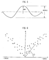
- Figure 3 illustrates both warpage and bow.
- Characterizations of surface topography using warpage and bow can be ambiguous as an infinite number of profile shapes would satisfy a particular warpage or bow. If warpage W and bow B are considered together as in a W/B ratio, the vagueness is reduced. If warpage measurements are plotted as a function of bow, a population of wafer data points appears as generally shown in Figure 4.
- the usefulness of this measurement is realized when test data is correlated with ⁇ which eliminates the complexities of using ratios involving a division by very small numbers or zero. With a few exceptions, wafers with ⁇ in the range 90° ⁇ 20° are generally those which are close to being almost flat.
- the task of correlating the main features of each map with device test data is achieved by considering only large scale variations of the wafer surface as the first order effect. In this treatment, small localized variations are neglected for simplicity.
- elevations are measured using the center of the wafer as the reference point.
- Surface elevations are measured using the center of the wafer as the reference point, which is also the origin of a cylindrical (Y, ⁇ ,r) coördinate system.
- Y is the elevation
- ⁇ is the angular displacement
- r is the normalized radius ( ⁇ r ⁇ 1).
- the average elevation of the wafer edge (Y e ) and at some intermediate position (Y s ) are determined for each radius as illustrated in Figure 5.
- C denotes the center of the wafer
- S an intermediate site
- E the edge of the wafer.
- a minimum of four equally spaced radii are characterized for a wafer. Elevations above the wafer center are positive and those below are negative (i.e., the sense is opposite of bow). These measurements are then used as boundary conditions for an analytical solution expressing the large scale surface topography as a function of distance from the wafer center.
- the solution is a approximated by assuming a power series solution.
- a map of Y e versus Y s for each wafer defines a population of data points. This plot usually appears as an oblong distribution as illustrated in Figure 6.
- the model constants are redefined in terms of Y s and ⁇ as follows:
- the model constants for each wafer are also mapped.
- the relative relationship of the model constants are defined by a model constant angle ⁇ where
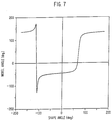
- equation (18) the dependence of ⁇ on ⁇ is shown in Figure 7.
- there are regions of the plot where ⁇ and ⁇ are almost exclusively invariant. In correlating test data to either ⁇ or ⁇ , there is sensitivity to small changes in either ⁇ or ⁇ in these regions of quasi invariance. It is therefore useful to correlate test data to both ⁇ and ⁇ which intersect the regions of Figure 7 critical to test data.
- the large scale surface topography is completely defined by ⁇ and the extent of complex bowing by M.
- Some additional fundamental definitions can also be made involving these terms.
- Surfaces are defined as proportionally similar if their ⁇ angles are identical although the values of M may be dissimilar. If the values of ⁇ are different, the surfaces are proportionally dissimilar.
- Simple topographies are defined as surfaces which are everywhere either convex or concave and usually occur within narrow ranges of ⁇ . It is generally observed that wafer surfaces with a large M (and large W/B ratios) will have topographies which are simple. A flat wafer is obtained in the limit as M ⁇ 0 for any shape angle.
- Topographies at various values of ⁇ in the range of from -180° to +180° are illustrated in Figure 8.
- surface inversions from convex to concave and vice versa
- the roots obtained are functionally dependant on the value of K.
- a set of similar branches account for the two negative critical angles with the same points of convergence.
- a sufficient angular spacing (e.g., >20°) between the bifurcated roots of each set is obtained for 0.3 ⁇ K ⁇ 0.85. Within this range, the maximum root separation in each set is almost 29° and occurs at K ⁇ 0.6 which is near the value used in the surface characterizations.
- the area of the inner circle is approximately equal to the annular region. This also gave a reasonable angular separation of the roots so that the influence of each critical shape angel on test data could be determined.
- a wafer may undergo a surface inversion resulting from process induced changes in ⁇ . These perturbations may arise during thermal processes or from processes which introduce mechanically applied stresses. These transitional surface instabilities can cause stress inversions (compressive/tensile) in silicon which may be localized near patterned structures.
- the map of Y e versus Y s in Figure 9 shows the oblong distribution of data points for the wafers along the critical inversion zones (IZ) as a reference.
- the left data points are surfaces which are generally convex while the right data points are generally concave.
- this population is shown to be angularly displaced by ⁇ 10° from the expected optimum (i.e., ⁇ 70°) which causes a larger overlap of one of the critical zones (IZ lines).
- the distribution also shows that an almost full spectrum of shapes exist at smaller values of M. As M increases, the range of ⁇ eventually becomes limited to those values associated with simple topographies. This indicates that the shape angle is dependent on M and wafer bow.
- Test results from a maze consisting of parallel isolation trench structures indicates that the EXP wafers had fewer wafers with low yield due to BVcc leakage.
- a correlation with bow and M prior to the trench CVD oxide shows that the 20 volt BVcc yield decreases with a reduction in convexity of both POR and EXP wafers.
- Figure 11 shows that the higher yield obtained with the EXP wafers from product A could be attributed to a larger population of convex wafers.
- EXP2 wafers had a lower yield than either EXP or POR wafers which can be attributed to a larger population of wafers with surface topographies near inversion zone states.
- a correlation with shape and model angles indicates that the maze yield of all wafers is influenced by the proximity of the wafer surfaces to critical inversion zone angles shown in Figures 12 and 13, respectively.
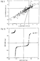
- the BVcc LLY is plotted as a function of the shape angle which was measured prior to the trench mask oxide process. The entire range of shape angles is not represented as these measurements were limited to only product A. However, this plot does show some indication that the isolation LLY is lowered by the proximity of wafer surfaces to critical shape angles. Critical shape angles occur at -124.7°, -96.1°, +55.3°, and +83.9°.
- Figure 13 shows the same LLY data base as a function of the model angle also measured prior to the trench mask CVD oxide.
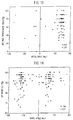
- the BVcbo LLY for both product types is plotted as a function of the shape angle measured prior to the trench mask CVD oxide process.
- the large data base in this plot shows clearly that the yield is lowered by the proximity of wafer surfaces near the critical shape angles at -124.7°, -96.1°, +55.3°, and +83.9°.
- Lower LLY levels are also evident for wafer surfaces near the critical model angles at -60.7°, -32.1°, +199.3°, and +147.9°, as shown in Figure 15.
- the coincident behavior of the LLY levels near the critical shape and model angles indicates that the junction leakage of discrete device structures is associated with the surface inversion zones characterized prior to the fabrication of the isolation structures.
- Figure 16 shows that BVcbo LLY is conditionally dependant on the degree of convex bowing.
- M the yield
- M the yield
- M the yield
- M the yield
- M the yield
- M the yield
- M the yield
- M the yield
- M the yield
- M the yield
- M the yield
- M the yield
- M the yield
- M the yield
- M the yield
- M the yield
- M the yield
- M is improved and apparently insensitive to the surface inversion phenomena. This threshold may be due to the lower stress limit required to generate defects.
- M the yield is statistically reduced as the effects of the surface inversions become apparent.
- M>M U ⁇ 18 ⁇ m BVcbo yield is improved. This is attributed to a decreasing population of wafers occupying inversion zone states as M is increased further.
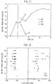
- Figure 17 shows that the CE and TX failure rate of EXP wafers (F exp ) is reduced and is dependent on failure rate level of the POR wafers (F por ).
- wafers with favorable surface topographies prior to the trench process can improve yield by moderating large variations in LLY.
- Leakage limited yield results obtained from the trench maze isolation and from discrete kerf transistor structures both indicate that M U is approximately 18 ⁇ m. While the LLY results obtained from the discrete transistor indicates that M L is approximately 4 ⁇ m, isolation maze results show that M L ⁇ 0. This difference indicates that wafers which are nearly flat will result in low trench maze yields which is believed to be caused by a sensitivity to unrelieved stresses localized at isolation structures in the silicon.
- the characterization of large scale wafer topography as described above is applied to improving device characteristics and yields in the manufacture large scale integrated (LSI) devices.
- the heights at the center, the edge and an intermediate point are measured on four or more, and preferably eight, equally spaced radii. This provides, for example, eight values each for Y s and Y e which are averaged.
- the shape angle ⁇ is computed using the following equation:
- the thus computed values of ⁇ and M are correlated with individual wafer characteristics as to device performance and yield. Based on these results, the wafer processing is controlled to provide optimal wafer characteristics.
Landscapes
- Physics & Mathematics (AREA)
- General Physics & Mathematics (AREA)
- Testing Or Measuring Of Semiconductors Or The Like (AREA)
- Testing Of Individual Semiconductor Devices (AREA)
Description
- The present invention generally relates to the manufacture of integrated circuits in silicon wafers and, more particularly, to the correlation of the large scale topography of a semiconductor wafer to the characteristics of devices subsequently formed on the wafer. Where significant correlations are found, the large scale topography of subsequent wafers are modified to optimize device characteristics and yield.
- In the manufacture of large scale integrated (LSI) circuits, there are various factors which contribute to increased circuit density. Among these are reductions in feature size and an increase in device and circuit complexity. The greater circuit densities are being achieved with the use of several types of transistors on a single chip, allowing for greater design flexibility. The varying transistor types as well as their closer proximity require improvements in device isolation. Current technology, however, does not explain isolation and device junction leakage related failures in some device structures. It is important to address this problem since it is an important factor in both increased circuit density and product yield.
- A study was made by the inventors to determine the effects of large scale surface topography (LST) which exist on product wafers prior to defining the isolation structures on leakage limited yields (LLY). Specific topographic configurations were characterized using a shape factor defined by the angle and magnitude of the bending pattern for each wafer. This shape factor was used to correlate LST with LLY. The results of the study showed that specific unfavorable LST configurations contribute to low test yields at trench maze, post Pt and K metal as well as final test yields. From these results, the inventors have concluded that these lower yields can be attributed to the stress induced defects which arise from unfavorable LST configurations.
- It is therefore an object of the present invention to provide a method of characterizing large scale wafer topography critical to device yields.
- It is another object of the invention to provide a method of modifying surface topography to more favorable configurations which optimize device characteristics and yield.
- According to the invention, a method is provided for determining the large scale topography of wafers by measuring wafer height, relative to a central reference point, at selected radial positions over the surface of the wafer. A shape angle, α, and shape magnitude, M, are computed based on these measurements. The α and M values for each wafer are correlated with device performance and yield.
- A model predicts the existence of four critical shapes where surface inversions may occur (convex to concave and vice versa) which may result in stress inversions (tensile to compressive and vice versa). Wafers are selected, using the characterization technique, which have unfavorable configurations at any point in the processing. The shape of these wafers is then altered to a favorable configuration before processing is continued. This is accomplished by producing a compensating non-uniform film on the backside of the wafer. This is achieved by the selective removal of the backside films or the addition of films typically used in semiconductor processing. By limiting this reconfiguration processing to the backside, the frontside can be left undisturbed.
- The foregoing and other objects, aspects and advantages will be better understood from the following detailed description of a preferred embodiment of the invention with reference to the drawings, in which:
- Figure 1 is a flow diagram showing the front end process of split lot comparison;
- Figure 2 is a topographic map of the surface of a silicon wafer, and Figure 2A is a three-dimensional projection of the topographic map;
- Figure 3 is a graph illustrating the definition of warpage and bow;
- Figure 4 is a graph showing the dependence of warpage on bow;
- Figure 5 is a graph showing measurements of relative elevations along a radius at an intermediate site and the edge of a wafer relative to the center;
- Figure 6 is a graph showing a map of data points defining the shape angle α and magnitude M;
- Figure 7 is a graph showing the theoretical model angle β versus shape angle α;
- Figure 8 is a family of graphs illustrating radial profiles of selected axially symmetric topographies;
- Figure 9 is a graph showing population (Ys, Ye) data prior to trench CVD oxidation;
- Figure 10 is a graph showing model angle, β, versus shape angle α illustrating the distribution of data points prior to trench CVD oxidation;
- Figure 11 is a graph showing the dependence of isolation maze BVcc LLY on wafer bow prior to trench CVD oxidation;
- Figure 12 is a graph showing the dependence of isolation maze LLY on shape angle, α, prior to trench CVD oxidation;
- Figure 13 is a graph showing the dependence of isolation maze LLY on mode angle, β, prior to trench CVD oxidation;
- Figure 14 is a graph showing the dependence of BVcbo LLY on shape angle, α, prior to trench CVD oxidation;
- Figure 15 is a graph showing the dependence of BVcbo LLY on model angle, β, prior to trench CVD oxidation;
- Figure 16 is a graph showing BVcbo LLY versus shape magnitude, M, prior to trench CVD oxidation;
- Figure 17 is a graph showing change in circuit failure rate due to EXP wafers versus failure rate for POR wafers for products A and B;
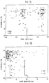
- Figure 18 is a graph showing the dependence of final test chip yield on wafer shape angle prior to trench CVD oxidation; and
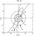
- Figure 19 is a graph showing the relationship of an arbitrary set of points to critical shape angles corresponding to surface inversion zones.
- A study of wafer surfaces prior to trench isolation shows that wafers with particular profile shapes have a higher incidence of leakage related failures in trench and device structures. These surfaces had been characterized after silicon epitaxy and oxide and nitride films had been grown. Subsequent removal of these nitride and oxide layers from the backside of the wafers using reactive ion etch (RIE) was found to decrease the wave convexity and often to a flat or concave state. Elimination of this backside etch leaves wafers in a more convex state prior to the chemical vapor deposition (CVD) oxide film growth which is used to define trench isolation structures.
- Wafers from two product types, referred to herein as product A and product B, with bipolar device structures using polycrystalline silicon filled trench (PST) isolation technology were used to assess the influence of surface topography and the backside etch process prior to trench CVD oxidation. The evaluation utilized six jobs which were split prior to the backside etch process. Half the wafers in each job received the process of record (POR) backside etch while the other experimental half (EXP) were not etched. In one job (product A), the experimental cell (EXP2) received only the frontside photoresist and strip processes. Figure 1 shows the process details used which compares the elimination of the backside etch with the POR. As shown in Figure 1, the surface topography, warpage and bow of each wafer were determined before and after the backside etch process and characterized again at the end of the master slice.
- The surface topographies were obtained from an automated interferometer using an optical HeNe laser. The output is a contour map showing elevations. A typical map is shown in Figure 2 and, as a three-dimensional projection, in Figure 2A. The characterization zone of such maps excludes ≃2mm of the wafer edge. The term "wafer edge" as used here refers to the edge of the characterization zone. Within this region, it is useful to describe surface topography in terms of wafer warpage and bow. By convention, warpage is defined as the maximum variation of the wafer surface. It is measured as the difference (always positive) between the highest and lowest elevation without regard to location. Wafer bow is defined as the elevation at the wafer center relative to a reference plane. As used herein, the reference plane is defined at the wafer edge as a best fit surface placing the wafer parallel to a reference prism. Positive bow denotes a generally convex surface and negative bow defines a concave surface. Figure 3 illustrates both warpage and bow.
- Characterizations of surface topography using warpage and bow can be ambiguous as an infinite number of profile shapes would satisfy a particular warpage or bow. If warpage W and bow B are considered together as in a W/B ratio, the vagueness is reduced. If warpage measurements are plotted as a function of bow, a population of wafer data points appears as generally shown in Figure 4. The W/B ratio can be used to define an angle

range 90°±20° are generally those which are close to being almost flat. Where Ω becomes almost invariant (for large |B|), the relationship of W to B is approximately fixed. This generally occurs when wafer surfaces are either everywhere convex or concave. Test data is plotted in Figure 4 with Ω to determine the sensitivity to surfaces which are nearly flat. Apart from this, Ω is not useful in identifying more complex large scale topographies. - Solid State Technology, vol. 23, n° 6, June '80, US;
pp 20,48 "Unique Computerized Laster Interferometer System Analyzes Wafer Flatness for 100% Inspection" by C. Synborsky describes a technique in the manufacture of integrated circuits, to test and sort wafers, according to 3 different user-selected parameters, one of which being the warpage measurement. - The task of correlating the main features of each map with device test data is achieved by considering only large scale variations of the wafer surface as the first order effect. In this treatment, small localized variations are neglected for simplicity. In this method, elevations are measured using the center of the wafer as the reference point. Surface elevations are measured using the center of the wafer as the reference point, which is also the origin of a cylindrical (Y, θ,r) coördinate system. In this notation, Y is the elevation, θ is the angular displacement, and r is the normalized radius (θ≤r≤1). From the topographical maps, the average elevation of the wafer edge (Ye) and at some intermediate position (Ys) are determined for each radius as illustrated in Figure 5. In Figure 5, C denotes the center of the wafer, S an intermediate site and E the edge of the wafer. The average elevation is defined at the edge (r=1) using


- A minimum of four equally spaced radii are characterized for a wafer. Elevations above the wafer center are positive and those below are negative (i.e., the sense is opposite of bow). These measurements are then used as boundary conditions for an analytical solution expressing the large scale surface topography as a function of distance from the wafer center.
- The general solution is derived by solving linear differential equation with constant coefficients of the form





- A map of Ye versus Ys for each wafer defines a population of data points. This plot usually appears as an oblong distribution as illustrated in Figure 6. The relative relationship between these measurements is defined by a shape angle, α, and magnitude, M, where


- Using the techniques described, the large scale surface topography is completely defined by α and the extent of complex bowing by M. Some additional fundamental definitions can also be made involving these terms. Surfaces are defined as proportionally similar if their α angles are identical although the values of M may be dissimilar. If the values of α are different, the surfaces are proportionally dissimilar. Simple topographies are defined as surfaces which are everywhere either convex or concave and usually occur within narrow ranges of α. It is generally observed that wafer surfaces with a large M (and large W/B ratios) will have topographies which are simple. A flat wafer is obtained in the limit as M → 0 for any shape angle.
- Topographies at various values of α in the range of from -180° to +180° are illustrated in Figure 8. In these graphs, surface inversions (from convex to concave and vice versa) are noted in regions which correspond to the corners shown in Figure 7. The critical values of α at which these surface inversions occur can be determined by solving for the roots of dβ/dα=1. The roots obtained are functionally dependant on the value of K. The two positive critical angles (roots) lie on a set of two bifurcated branch functions which converge at K=0 and K=1. A set of similar branches account for the two negative critical angles with the same points of convergence. A sufficient angular spacing (e.g., >20°) between the bifurcated roots of each set is obtained for 0.3<K<0.85. Within this range, the maximum root separation in each set is almost 29° and occurs at K≃0.6 which is near the value used in the surface characterizations. For K=0,1, the critical shape angles approach simple surface topographies which limits the usefulness of the method in identifying potential surface inversion states. Using K=2/3 was found to be convenient in characterizing a large number of wafer surfaces. For this value of K, the area of the inner circle is approximately equal to the annular region. This also gave a reasonable angular separation of the roots so that the influence of each critical shape angel on test data could be determined.
- If α is close to one of these critical values, a wafer may undergo a surface inversion resulting from process induced changes in α. These perturbations may arise during thermal processes or from processes which introduce mechanically applied stresses. These transitional surface instabilities can cause stress inversions (compressive/tensile) in silicon which may be localized near patterned structures.
- The backside nitride etch process prior to the deep trench CVD oxidation generally reduced wafer convexity by 5 to 15 µm in the bow measurements. As a result, many of these POR wafers were nearly flat or in a concave state which could introduce corresponding compressive stress effects, particularly near trench and device regions. The elimination of this process left the bow of EXP wafers in a more convex state (10 to 30 µm) on both product types. Bow measurements of EXP2 wafers indicated that photoresist related processes (without RIE) reduced convexity slightly by 2 to 3 µm. This shift in bow is attributed to the plasma etching of the photoresist film. Also, the shape and mode angles of the EXP2 wafers were uniquely different from EXP wafers in that these angles were shifted towards one of the inversion zones.
- The map of Ye versus Ys in Figure 9 shows the oblong distribution of data points for the wafers along the critical inversion zones (IZ) as a reference. In Figure 9, the left data points are surfaces which are generally convex while the right data points are generally concave. Using the Ys axis as a reference, this population is shown to be angularly displaced by ≃10° from the expected optimum (i.e., α≃70°) which causes a larger overlap of one of the critical zones (IZ lines). The distribution also shows that an almost full spectrum of shapes exist at smaller values of M. As M increases, the range of α eventually becomes limited to those values associated with simple topographies. This indicates that the shape angle is dependent on M and wafer bow. Using equations (16), (17) and (18), the model constants (a,b) and the model angle, β, were then calculated for each wafer. The plot of β versus α in Figure 10 shows a distribution which populates almost the entire range shown in the theoretical curve of Figure 7. Data points located near the corners of Figure 10 correspond to points near the IZ lines in Figure 9.
- Test results from a maze consisting of parallel isolation trench structures indicates that the EXP wafers had fewer wafers with low yield due to BVcc leakage. A correlation with bow and M prior to the trench CVD oxide shows that the 20 volt BVcc yield decreases with a reduction in convexity of both POR and EXP wafers. Figure 11 shows that the higher yield obtained with the EXP wafers from product A could be attributed to a larger population of convex wafers. However, EXP2 wafers had a lower yield than either EXP or POR wafers which can be attributed to a larger population of wafers with surface topographies near inversion zone states.
- A correlation with shape and model angles indicates that the maze yield of all wafers is influenced by the proximity of the wafer surfaces to critical inversion zone angles shown in Figures 12 and 13, respectively. In Figure 12, the BVcc LLY is plotted as a function of the shape angle which was measured prior to the trench mask oxide process. The entire range of shape angles is not represented as these measurements were limited to only product A. However, this plot does show some indication that the isolation LLY is lowered by the proximity of wafer surfaces to critical shape angles. Critical shape angles occur at -124.7°, -96.1°, +55.3°, and +83.9°. In a similar plot, Figure 13 shows the same LLY data base as a function of the model angle also measured prior to the trench mask CVD oxide. This plot shows lower yields for those wafer surfaces which are near critical model angles at -60.7°, -32.1°, +119.3°, and +147.9°. The coincident lower LLY levels near the critical shape and model angles are associated with the surface inversion zones which correspond to the corners shown in Figure 7.
- Measurements at post Pt test indicated that all wafers had simple convex topographies with no significant differences between EXP or POR wafers within a particular product type. However, product B wafers were significantly less convex (3 to 7µm) than product A wafers (12 to 25µm). As the two product types have similar processes, this difference is attributed to differences in the density of trench isolation structures.
- Discrete transistor structures in the kerf were tested after the master slice processes to assess transistor LLY. In this test, the collector to base break down voltage (BVcbo) with the emitter open was measured at 10 µA on fifty sites per wafer. These results show that the BVcbo LLY levels were generally improved with the EXP wafers. However, In contrast to the low isolation maze LLY, the EXP2 wafers had a slightly higher BVcbo yield than POR wafers in the same job. Correlations with shape and model angles prior to trench CVD oxidation shows that the BVcbo LLY of all wafers, regardless of product type, were influenced by surface inversions as shown in Figures 14 and 15.
- In Figure 14, the BVcbo LLY for both product types is plotted as a function of the shape angle measured prior to the trench mask CVD oxide process. The large data base in this plot shows clearly that the yield is lowered by the proximity of wafer surfaces near the critical shape angles at -124.7°, -96.1°, +55.3°, and +83.9°. Lower LLY levels are also evident for wafer surfaces near the critical model angles at -60.7°, -32.1°, +199.3°, and +147.9°, as shown in Figure 15. The coincident behavior of the LLY levels near the critical shape and model angles indicates that the junction leakage of discrete device structures is associated with the surface inversion zones characterized prior to the fabrication of the isolation structures.
- Figure 16 shows that BVcbo LLY is conditionally dependant on the degree of convex bowing. For wafers with M<ML ≃ 4 µm, the yield is improved and apparently insensitive to the surface inversion phenomena. This threshold may be due to the lower stress limit required to generate defects. For larger values of M, BVcbo yield is statistically reduced as the effects of the surface inversions become apparent. For M>MU ≃ 18 µm, BVcbo yield is improved. This is attributed to a decreasing population of wafers occupying inversion zone states as M is increased further.
- Device chains consisting of parallel transistor circuit cells using 1.5x2 µm emitters were tested using a sample of twelve sites per wafer. In this test, the junction leakage parameters of trench (TR) isolation structures and transistor (TX) structures were analyzed as exclusive categories. For both product types, the TR LLY results generally indicated that the EXP wafers were comparable to those for the POR cell as only slight improvements were noted. Larger improvements were found in the TX LLY in which the major TX failure mechanism was collector to emitter (CE) leakage in both product types. The average circuit failure rate (F) for each chain and product type was determined from the LLY(Y) using

- Final test yields from both product types plotted as a function shape angle measured prior to trench CVD oxidation are shown in Figure 18. In this figure, wafers have been sorted by their proximity (±10°) to critical shape angles. In comparison to wafers in noncritical zones, wafers near the inversion zones have a tendency to have reduced chip yields.
- These results can be described by the phenomenological model in Figure 19. In this illustration, the relationship of an arbitrary set of data points (Ys, Ye) to the critical inversion zone (IZ) angles is shown. Given any M as indicated, a population of wafers can be found which belong to regions which are in proximity to the inversion zones. Region dM at M contains a subset of points (wafers) in proximity to IZ lines, as shown. LLY improves for M<ML due to stress threshold effect. LLY reduced for ML<M<MU due to surface inversions. Decreasing the subset of points near IZ for M>MU improves yield. MU is varied by small rotations of set {Ys, Ye} around the origin. MU is minimum for a narrow set and centering between IZ regions.
- Leakage limited yield results obtained from the trench maze isolation and from discrete kerf transistor structures both indicate that MU is approximately 18 µm. While the LLY results obtained from the discrete transistor indicates that ML is approximately 4 µm, isolation maze results show that ML<0. This difference indicates that wafers which are nearly flat will result in low trench maze yields which is believed to be caused by a sensitivity to unrelieved stresses localized at isolation structures in the silicon.
- The characterization of large scale wafer topography as described above is applied to improving device characteristics and yields in the manufacture large scale integrated (LSI) devices.
First, the heights at the center, the edge and an intermediate point are measured on four or more, and preferably eight, equally spaced radii. This provides, for example, eight values each for Ys and Ye which are averaged. Then the shape angle α is computed using the following equation:

- While the invention has been described in terms of a single preferred embodiment, those skilled in the art will recognize that the invention can be practiced with modification within the scope of the appended claims.
Claims (2)
- A method of characterization of large scale wafer topography in the manufacture of manufactured large scale integrated semiconductor devices comprising the steps of:measuring the heights at the center, the edge and an intermediate point on a plurality of radii on the wafer to obtain a plurality of values each for Ys, the height of the intermediate point relative to the center, and Ye, the height of the edge relative to the center;averaging the plurality of values Ys and Ye;computing the shape angle computed using the following equation:
 computing the shape magnitude M using the following equation:
 correlating the computed values of α and M with individual wafer characteristics as to device performance and yield; andcontrolling wafer processing to provide optimal wafer yield and leakage characteristics.
 - The method recited in claim 1 wherein measurements are taken along at least four equally spaced radii over the surface of the wafer.
Applications Claiming Priority (2)
| Application Number | Priority Date | Filing Date | Title |
|---|---|---|---|
| US07/774,084 US5319570A (en) | 1991-10-09 | 1991-10-09 | Control of large scale topography on silicon wafers |
| US774084 | 1991-10-09 |
Publications (2)
| Publication Number | Publication Date |
|---|---|
| EP0537099A1 EP0537099A1 (en) | 1993-04-14 |
| EP0537099B1 true EP0537099B1 (en) | 1996-01-03 |
Family
ID=25100204
Family Applications (1)
| Application Number | Title | Priority Date | Filing Date |
|---|---|---|---|
| EP92480126A Expired - Lifetime EP0537099B1 (en) | 1991-10-09 | 1992-09-11 | Control of large scale topography on silicon wafers |
Country Status (4)
| Country | Link |
|---|---|
| US (1) | US5319570A (en) |
| EP (1) | EP0537099B1 (en) |
| JP (1) | JPH0779120B2 (en) |
| DE (1) | DE69207330T2 (en) |
Families Citing this family (20)
| Publication number | Priority date | Publication date | Assignee | Title |
|---|---|---|---|---|
| US5562770A (en) * | 1994-11-22 | 1996-10-08 | International Business Machines Corporation | Semiconductor manufacturing process for low dislocation defects |
| US5636133A (en) * | 1995-05-19 | 1997-06-03 | International Business Machines Corporation | Efficient generation of fill shapes for chips and packages |
| US5910898A (en) * | 1995-12-14 | 1999-06-08 | Viewlogic Systems, Inc. | Circuit design methods and tools |
| US5960107A (en) * | 1995-12-28 | 1999-09-28 | Vlsi Technology, Inc. | Method for verifying an average topography height function of a photostepper |
| US6247853B1 (en) * | 1998-05-26 | 2001-06-19 | International Business Machines Corporation | Incremental method for critical area and critical region computation of via blocks |
| US6785413B1 (en) | 1999-08-24 | 2004-08-31 | International Business Machines Corporation | Rapid defect analysis by placement of tester fail data |
| US6630426B1 (en) | 2000-01-12 | 2003-10-07 | Teracomm Research Inc. | Method of increasing the critical temperature of a high critical temperature superconducting film and a superconducting structure made using the method |
| US6569249B1 (en) | 2000-04-18 | 2003-05-27 | Clemson University | Process for forming layers on substrates |
| DE10044162C2 (en) * | 2000-05-11 | 2002-12-05 | Wacker Siltronic Halbleitermat | Standard for a nanotopography device and method for producing the standard |
| US6434725B1 (en) * | 2000-06-26 | 2002-08-13 | Infineon Technologies Richmond, Lp | Method and system for semiconductor testing using yield correlation between global and class parameters |
| DE10056261A1 (en) * | 2000-11-14 | 2002-05-29 | Infineon Technologies Ag | Method for producing an integrated semiconductor component |
| US7657339B1 (en) * | 2005-10-14 | 2010-02-02 | GlobalFoundries, Inc. | Product-related feedback for process control |
| US7957827B2 (en) * | 2007-12-27 | 2011-06-07 | United Microelectronics Corp. | Method of controlling statuses of wafers |
| JP5384091B2 (en) * | 2008-12-11 | 2014-01-08 | アズビル株式会社 | Inspection data management system and inspection data management method |
| US8927334B2 (en) | 2012-09-25 | 2015-01-06 | International Business Machines Corporation | Overcoming chip warping to enhance wetting of solder bumps and flip chip attaches in a flip chip package |
| US9613915B2 (en) | 2014-12-02 | 2017-04-04 | International Business Machines Corporation | Reduced-warpage laminate structure |
| TWI608364B (en) * | 2015-01-26 | 2017-12-11 | 華邦電子股份有限公司 | Method for calculating yield loss of test pattern of wafer |
| CN110096754A (en) * | 2019-04-04 | 2019-08-06 | 西北工业大学 | The mechanic equivalent method of Crystal Nickel-based Superalloy component surface pattern |
| TWI770906B (en) * | 2021-03-26 | 2022-07-11 | 環球晶圓股份有限公司 | Wafer surface defect inspection method and apparatus thereof |
| JP7746951B2 (en) * | 2022-09-21 | 2025-10-01 | 株式会社Sumco | Wafer shape modeling method and wafer manufacturing method |
Family Cites Families (9)
| Publication number | Priority date | Publication date | Assignee | Title |
|---|---|---|---|---|
| US3751647A (en) * | 1971-09-22 | 1973-08-07 | Ibm | Semiconductor and integrated circuit device yield modeling |
| US3729966A (en) * | 1972-02-02 | 1973-05-01 | Ibm | Apparatus for contouring the surface of thin elements |
| GB2037464B (en) * | 1978-12-14 | 1982-11-24 | Rank Organisation Ltd | Method for analysing variables |
| US4272196A (en) * | 1979-01-12 | 1981-06-09 | Lasag S.A. | Optical sizing mask and process |
| JPS5744807A (en) * | 1980-08-29 | 1982-03-13 | Hitachi Ltd | Flatness measuring apparatus |
| US4422764A (en) * | 1980-12-12 | 1983-12-27 | The University Of Rochester | Interferometer apparatus for microtopography |
| DE3710365A1 (en) * | 1987-03-28 | 1988-10-13 | Messerschmitt Boelkow Blohm | METHOD FOR REPRODUCIBLE FORMATION OF MATERIAL LAYERS AND / OR TREATMENT OF SEMICONDUCTOR MATERIAL LAYERS |
| US5067101A (en) * | 1988-11-29 | 1991-11-19 | Mitsubishi Denki Kabushiki Kaisha | Topography simulation method |
| US5070469A (en) * | 1988-11-29 | 1991-12-03 | Mitsubishi Denki Kabushiki Kaisha | Topography simulation method |
-
1991
- 1991-10-09 US US07/774,084 patent/US5319570A/en not_active Expired - Fee Related
-
1992
- 1992-08-13 JP JP4216193A patent/JPH0779120B2/en not_active Expired - Lifetime
- 1992-09-11 EP EP92480126A patent/EP0537099B1/en not_active Expired - Lifetime
- 1992-09-11 DE DE69207330T patent/DE69207330T2/en not_active Expired - Fee Related
Also Published As
| Publication number | Publication date |
|---|---|
| JPH0779120B2 (en) | 1995-08-23 |
| EP0537099A1 (en) | 1993-04-14 |
| DE69207330D1 (en) | 1996-02-15 |
| DE69207330T2 (en) | 1996-07-11 |
| US5319570A (en) | 1994-06-07 |
| JPH05235133A (en) | 1993-09-10 |
Similar Documents
| Publication | Publication Date | Title |
|---|---|---|
| US5319570A (en) | Control of large scale topography on silicon wafers | |
| EP0212219B1 (en) | Visibility enhancement of first order alignment marks | |
| EP0566218A2 (en) | Method for finding a preferred spot for a laser beam of a laser beam interferometer and laser interferometer apparatus | |
| US20020009814A1 (en) | Film thickness measuring method of member to be processed using emission spectroscopy and processing method of the member using the measuring method | |
| EP0059039B1 (en) | Method of measuring carrier distribution | |
| KR100969636B1 (en) | Process control to improve wafer uniformity using integrated or standalone metrology | |
| US5684301A (en) | Monocrystalline test structures, and use for calibrating instruments | |
| KR910009611B1 (en) | Trench etching method | |
| US6372082B1 (en) | Method and apparatus for semiconductor device fabrication | |
| CN113611626B (en) | A method for online detection of silicon trench etching depth | |
| US4510798A (en) | Shallow junction depth measurement method | |
| US6949387B2 (en) | Method of designing a semiconductor device | |
| US7039488B2 (en) | Method of determining remaining film thickness in polishing process | |
| JPH08213369A (en) | Method for manufacturing semiconductor device | |
| EP1218934B1 (en) | Method for determining the endpoint of etch process steps | |
| Hedlund et al. | Method for the determination of the angular dependence during dry etching | |
| Conru | Measuring small‐area Si/SiO2 interface stress with SEM | |
| US4439268A (en) | Orientation of INP substrate wafers | |
| CN108063098A (en) | The analog detecting method of round and smooth degree at the top of active area | |
| US6121060A (en) | Method of measuring a concentration profile | |
| JPH02143543A (en) | Evaluation of transition region of epitaxial wafer | |
| Morris | Some device applications of spreading resistance measurements on epitaxial silicon | |
| US6862545B1 (en) | Linewidth measurement tool calibration method employing linewidth standard | |
| US12397394B1 (en) | Method and device for determining parameters of near-surface dielectric layer in wafer grinding scene | |
| US5456117A (en) | Pressure sensor apparatus and method of manufacturing wherein the silicon-crystal substrate of the sensor has inclined crystallographic axes and gage resistors formed in a cavity of the substrate |
Legal Events
| Date | Code | Title | Description |
|---|---|---|---|
| PUAI | Public reference made under article 153(3) epc to a published international application that has entered the european phase |
Free format text: ORIGINAL CODE: 0009012 |
|
| AK | Designated contracting states |
Kind code of ref document: A1 Designated state(s): DE FR GB |
|
| 17P | Request for examination filed |
Effective date: 19930819 |
|
| 17Q | First examination report despatched |
Effective date: 19940927 |
|
| GRAA | (expected) grant |
Free format text: ORIGINAL CODE: 0009210 |
|
| AK | Designated contracting states |
Kind code of ref document: B1 Designated state(s): DE FR GB |
|
| REF | Corresponds to: |
Ref document number: 69207330 Country of ref document: DE Date of ref document: 19960215 |
|
| ET | Fr: translation filed | ||
| PGFP | Annual fee paid to national office [announced via postgrant information from national office to epo] |
Ref country code: GB Payment date: 19960827 Year of fee payment: 5 |
|
| PLBE | No opposition filed within time limit |
Free format text: ORIGINAL CODE: 0009261 |
|
| 26N | No opposition filed | ||
| PG25 | Lapsed in a contracting state [announced via postgrant information from national office to epo] |
Ref country code: DE Effective date: 19970603 |
|
| PG25 | Lapsed in a contracting state [announced via postgrant information from national office to epo] |
Ref country code: FR Effective date: 19970630 |
|
| REG | Reference to a national code |
Ref country code: FR Ref legal event code: ST |
|
| REG | Reference to a national code |
Ref country code: FR Ref legal event code: ST |
|
| PG25 | Lapsed in a contracting state [announced via postgrant information from national office to epo] |
Ref country code: GB Free format text: LAPSE BECAUSE OF NON-PAYMENT OF DUE FEES Effective date: 19970911 |
|
| GBPC | Gb: european patent ceased through non-payment of renewal fee |
Effective date: 19970911 |