EP0531298B1 - Electrochromic, electroluminescent and electrochemiluminescent displays - Google Patents
Electrochromic, electroluminescent and electrochemiluminescent displays Download PDFInfo
- Publication number
- EP0531298B1 EP0531298B1 EP91905939A EP91905939A EP0531298B1 EP 0531298 B1 EP0531298 B1 EP 0531298B1 EP 91905939 A EP91905939 A EP 91905939A EP 91905939 A EP91905939 A EP 91905939A EP 0531298 B1 EP0531298 B1 EP 0531298B1
- Authority
- EP
- European Patent Office
- Prior art keywords
- electrodes
- pair
- bus bars
- electrochromic
- substrate
- Prior art date
- Legal status (The legal status is an assumption and is not a legal conclusion. Google has not performed a legal analysis and makes no representation as to the accuracy of the status listed.)
- Expired - Lifetime
Links
Images


Classifications
-
- G—PHYSICS
- G02—OPTICS
- G02F—OPTICAL DEVICES OR ARRANGEMENTS FOR THE CONTROL OF LIGHT BY MODIFICATION OF THE OPTICAL PROPERTIES OF THE MEDIA OF THE ELEMENTS INVOLVED THEREIN; NON-LINEAR OPTICS; FREQUENCY-CHANGING OF LIGHT; OPTICAL LOGIC ELEMENTS; OPTICAL ANALOGUE/DIGITAL CONVERTERS
- G02F1/00—Devices or arrangements for the control of the intensity, colour, phase, polarisation or direction of light arriving from an independent light source, e.g. switching, gating or modulating; Non-linear optics
- G02F1/01—Devices or arrangements for the control of the intensity, colour, phase, polarisation or direction of light arriving from an independent light source, e.g. switching, gating or modulating; Non-linear optics for the control of the intensity, phase, polarisation or colour
- G02F1/15—Devices or arrangements for the control of the intensity, colour, phase, polarisation or direction of light arriving from an independent light source, e.g. switching, gating or modulating; Non-linear optics for the control of the intensity, phase, polarisation or colour based on an electrochromic effect
- G02F1/153—Constructional details
- G02F1/155—Electrodes
-
- F—MECHANICAL ENGINEERING; LIGHTING; HEATING; WEAPONS; BLASTING
- F21—LIGHTING
- F21K—NON-ELECTRIC LIGHT SOURCES USING LUMINESCENCE; LIGHT SOURCES USING ELECTROCHEMILUMINESCENCE; LIGHT SOURCES USING CHARGES OF COMBUSTIBLE MATERIAL; LIGHT SOURCES USING SEMICONDUCTOR DEVICES AS LIGHT-GENERATING ELEMENTS; LIGHT SOURCES NOT OTHERWISE PROVIDED FOR
- F21K2/00—Non-electric light sources using luminescence; Light sources using electrochemiluminescence
- F21K2/06—Non-electric light sources using luminescence; Light sources using electrochemiluminescence using chemiluminescence
- F21K2/08—Non-electric light sources using luminescence; Light sources using electrochemiluminescence using chemiluminescence activated by an electric field, i.e. electrochemiluminescence
-
- G—PHYSICS
- G02—OPTICS
- G02F—OPTICAL DEVICES OR ARRANGEMENTS FOR THE CONTROL OF LIGHT BY MODIFICATION OF THE OPTICAL PROPERTIES OF THE MEDIA OF THE ELEMENTS INVOLVED THEREIN; NON-LINEAR OPTICS; FREQUENCY-CHANGING OF LIGHT; OPTICAL LOGIC ELEMENTS; OPTICAL ANALOGUE/DIGITAL CONVERTERS
- G02F1/00—Devices or arrangements for the control of the intensity, colour, phase, polarisation or direction of light arriving from an independent light source, e.g. switching, gating or modulating; Non-linear optics
- G02F1/01—Devices or arrangements for the control of the intensity, colour, phase, polarisation or direction of light arriving from an independent light source, e.g. switching, gating or modulating; Non-linear optics for the control of the intensity, phase, polarisation or colour
- G02F1/15—Devices or arrangements for the control of the intensity, colour, phase, polarisation or direction of light arriving from an independent light source, e.g. switching, gating or modulating; Non-linear optics for the control of the intensity, phase, polarisation or colour based on an electrochromic effect
- G02F1/1503—Devices or arrangements for the control of the intensity, colour, phase, polarisation or direction of light arriving from an independent light source, e.g. switching, gating or modulating; Non-linear optics for the control of the intensity, phase, polarisation or colour based on an electrochromic effect caused by oxidation-reduction reactions in organic liquid solutions, e.g. viologen solutions
-
- G—PHYSICS
- G02—OPTICS
- G02F—OPTICAL DEVICES OR ARRANGEMENTS FOR THE CONTROL OF LIGHT BY MODIFICATION OF THE OPTICAL PROPERTIES OF THE MEDIA OF THE ELEMENTS INVOLVED THEREIN; NON-LINEAR OPTICS; FREQUENCY-CHANGING OF LIGHT; OPTICAL LOGIC ELEMENTS; OPTICAL ANALOGUE/DIGITAL CONVERTERS
- G02F1/00—Devices or arrangements for the control of the intensity, colour, phase, polarisation or direction of light arriving from an independent light source, e.g. switching, gating or modulating; Non-linear optics
- G02F1/01—Devices or arrangements for the control of the intensity, colour, phase, polarisation or direction of light arriving from an independent light source, e.g. switching, gating or modulating; Non-linear optics for the control of the intensity, phase, polarisation or colour
- G02F1/15—Devices or arrangements for the control of the intensity, colour, phase, polarisation or direction of light arriving from an independent light source, e.g. switching, gating or modulating; Non-linear optics for the control of the intensity, phase, polarisation or colour based on an electrochromic effect
- G02F1/1514—Devices or arrangements for the control of the intensity, colour, phase, polarisation or direction of light arriving from an independent light source, e.g. switching, gating or modulating; Non-linear optics for the control of the intensity, phase, polarisation or colour based on an electrochromic effect characterised by the electrochromic material, e.g. by the electrodeposited material
- G02F1/1523—Devices or arrangements for the control of the intensity, colour, phase, polarisation or direction of light arriving from an independent light source, e.g. switching, gating or modulating; Non-linear optics for the control of the intensity, phase, polarisation or colour based on an electrochromic effect characterised by the electrochromic material, e.g. by the electrodeposited material comprising inorganic material
- G02F1/1525—Devices or arrangements for the control of the intensity, colour, phase, polarisation or direction of light arriving from an independent light source, e.g. switching, gating or modulating; Non-linear optics for the control of the intensity, phase, polarisation or colour based on an electrochromic effect characterised by the electrochromic material, e.g. by the electrodeposited material comprising inorganic material characterised by a particular ion transporting layer, e.g. electrolyte
-
- G—PHYSICS
- G02—OPTICS
- G02F—OPTICAL DEVICES OR ARRANGEMENTS FOR THE CONTROL OF LIGHT BY MODIFICATION OF THE OPTICAL PROPERTIES OF THE MEDIA OF THE ELEMENTS INVOLVED THEREIN; NON-LINEAR OPTICS; FREQUENCY-CHANGING OF LIGHT; OPTICAL LOGIC ELEMENTS; OPTICAL ANALOGUE/DIGITAL CONVERTERS
- G02F1/00—Devices or arrangements for the control of the intensity, colour, phase, polarisation or direction of light arriving from an independent light source, e.g. switching, gating or modulating; Non-linear optics
- G02F1/01—Devices or arrangements for the control of the intensity, colour, phase, polarisation or direction of light arriving from an independent light source, e.g. switching, gating or modulating; Non-linear optics for the control of the intensity, phase, polarisation or colour
- G02F1/15—Devices or arrangements for the control of the intensity, colour, phase, polarisation or direction of light arriving from an independent light source, e.g. switching, gating or modulating; Non-linear optics for the control of the intensity, phase, polarisation or colour based on an electrochromic effect
- G02F1/1514—Devices or arrangements for the control of the intensity, colour, phase, polarisation or direction of light arriving from an independent light source, e.g. switching, gating or modulating; Non-linear optics for the control of the intensity, phase, polarisation or colour based on an electrochromic effect characterised by the electrochromic material, e.g. by the electrodeposited material
- G02F1/1516—Devices or arrangements for the control of the intensity, colour, phase, polarisation or direction of light arriving from an independent light source, e.g. switching, gating or modulating; Non-linear optics for the control of the intensity, phase, polarisation or colour based on an electrochromic effect characterised by the electrochromic material, e.g. by the electrodeposited material comprising organic material
- G02F2001/1517—Cyano complex compounds, e.g. Prussian blue
-
- G—PHYSICS
- G02—OPTICS
- G02F—OPTICAL DEVICES OR ARRANGEMENTS FOR THE CONTROL OF LIGHT BY MODIFICATION OF THE OPTICAL PROPERTIES OF THE MEDIA OF THE ELEMENTS INVOLVED THEREIN; NON-LINEAR OPTICS; FREQUENCY-CHANGING OF LIGHT; OPTICAL LOGIC ELEMENTS; OPTICAL ANALOGUE/DIGITAL CONVERTERS
- G02F1/00—Devices or arrangements for the control of the intensity, colour, phase, polarisation or direction of light arriving from an independent light source, e.g. switching, gating or modulating; Non-linear optics
- G02F1/01—Devices or arrangements for the control of the intensity, colour, phase, polarisation or direction of light arriving from an independent light source, e.g. switching, gating or modulating; Non-linear optics for the control of the intensity, phase, polarisation or colour
- G02F1/15—Devices or arrangements for the control of the intensity, colour, phase, polarisation or direction of light arriving from an independent light source, e.g. switching, gating or modulating; Non-linear optics for the control of the intensity, phase, polarisation or colour based on an electrochromic effect
- G02F1/153—Constructional details
- G02F1/155—Electrodes
- G02F2001/1555—Counter electrode
-
- G—PHYSICS
- G02—OPTICS
- G02F—OPTICAL DEVICES OR ARRANGEMENTS FOR THE CONTROL OF LIGHT BY MODIFICATION OF THE OPTICAL PROPERTIES OF THE MEDIA OF THE ELEMENTS INVOLVED THEREIN; NON-LINEAR OPTICS; FREQUENCY-CHANGING OF LIGHT; OPTICAL LOGIC ELEMENTS; OPTICAL ANALOGUE/DIGITAL CONVERTERS
- G02F1/00—Devices or arrangements for the control of the intensity, colour, phase, polarisation or direction of light arriving from an independent light source, e.g. switching, gating or modulating; Non-linear optics
- G02F1/01—Devices or arrangements for the control of the intensity, colour, phase, polarisation or direction of light arriving from an independent light source, e.g. switching, gating or modulating; Non-linear optics for the control of the intensity, phase, polarisation or colour
- G02F1/15—Devices or arrangements for the control of the intensity, colour, phase, polarisation or direction of light arriving from an independent light source, e.g. switching, gating or modulating; Non-linear optics for the control of the intensity, phase, polarisation or colour based on an electrochromic effect
- G02F1/153—Constructional details
- G02F1/155—Electrodes
- G02F2001/1557—Side by side arrangements of working and counter electrodes
Definitions
- the present invention relates to electrically reconfigurable displays and particularly to electrochromic, electroluminescent and electrochemiluminescent displays.
- emissive display systems are based on the generation of light, while the non-emissive display systems are based on the modulation of the ambient light.
- liquid crystal display wherein the property of certain materials to align themselves with an electric field is used to create a display.
- liquid crystals are widely used, they have the disadvantage of having a limited viewing angle, relatively low contrast and limited resolution.
- electrical addressing of liquid crystal arrays for high resolution applications generally requires an active display, that is, a display array having a thin-film transistor associated with each picture element. This requirement tends to increase the manufacturing cost and complexity of liquid crystal arrays, and to limit the minimum practical size of each picture element of such arrays.
- the need for precise control over the thickness of the space which is occupied by the liquid crystaline material between the front and the rear electrodes puts a limit on the maximum size of each picture element.
- electrochromic materials Some efforts have been made to make non-emissive displays using electrochromic materials. It is known that certain substances reversibly change their electromagnetic radiation absorption characteristics (i.e., color) when their redox state is changed, a property generally referred to as electrochromism.
- electrochromism One well-known example is tungsten trioxide (WO 3 ), which reversibly changes from pale yellow to deep blue when it is reduced.
- an electrochromic display matrix wherein electrochromic material is deposited on spaced apart parallel strips of transparent conductive material. These strips criss-cross with spaced apart transparent conductive strips, each of which is covered with an ion-conductive material, with the side of the strips having the electrochromic material facing the ion-conductive material side of the criss-crossed strips. A non-conductive paint is included between ion-conductive material covering the strips.
- the arrangement of electrochromic elements sandwiched between conductive strips requires the use of transparent conductive material, such as tin oxide (SnO 2 ), which has considerably lower conductivity than opaque metallic conductors, such as gold. Still further, the resolution obtainable with this proposed construction has been limited to strips in the range of 0.017 inches with a separation distance in the range of 0.003 inches, which does not significantly improve over the resolution currently available with liquid crystal technology.
- transparent conductive material such as tin oxide (SnO 2 )
- opaque metallic conductors such as gold
- Emissive displays include cathode ray tubes, semiconductor based light emitting diode arrays, electroluminescent arrays and electrochemiluminescent arrays.
- Conventional electroluminescent displays use the sandwich configuration with criss-crossed matrix addressed electrodes.
- Such an electroluminescent display is disclosed, for example in T. Sutela, Displays , April 1984, "Thin film electroluminescent displays produced by atomic layers", p. 73-78.
- this configuration requires the use of relatively low conductivity transparent electrodes for at least the top substrate. Because electroluminescent displays require considerable power, the relatively low conductivity of the transparent conductors is a significant limitation.
- Electrochemiluminescent displays operate on the principle that certain substances have stable oxidized and reduced forms that can react with each other in an annihilation fashion to yield the neutral form of the substance and one photon of light.
- the electrochemiluminescent substance is mixed into an electrolyte, and a bias is cyclically applied to emersed electrodes to obtain the oxidized and reduced forms, which then diffuse toward one another to cause annihilation and light.
- Electrochemiluminescent displays in the conventional sandwich configuration suffer from the same low conductivity electrode limitation as electroluminescent displays.
- electrochemiluminescent displays suffer from the difficulty of eliminating cross-talk between the pixels in matrix addressed displays due to the presence of the electrolyte, as in prior art electrochromic displays.
- the manufacture of integrated circuits by conventional photolithographic techniques involves the making of a group of several patterns, one for each photolithographic step. During manufacture of the integrated circuit, the substrate covered with a photoresist is exposed with light shone through one of these patterns. Then, after subsequent manufacturing steps, the substrate is exposed through another of the patterns. The making of and setting up of these patterns is time-consuming and expensive.
- US-A-4547046 discloses an electrochromic display device for use in automobiles, etc. comprising a plurality of mutually parallel strip-shaped display electrodes, a plurality of mutually parallel strip-shaped opposite electrodes, electrochemically-color-developing solid layers, solid electrolyte layers as intermediate layers, and an electrically insulating layer.
- the display electrodes and the opposite electrodes are arranged so as to three-dimensionally intersect each other.
- the electrochemically-color-developing solid layers and the solid electrolyte layers are present only at the spaces formed by the intersection between the display electrodes and the opposite electrodes.
- the electrically insulating layer occupies all portions other than the electrodes, electrochemically-color-developing solid layers and solid electrolyte layers within the device.
- US-A-3634714 discloses a matrix addressable electroluminescent device comprising a substrate member having electrode receiving upper and lower surfaces with a first plurality of individual relatively spaced ribbon electrodes secured to the upper surface of said substrate and forming a pattern array thereon, and a second plurality of individual spaced ribbon electrodes secured to the lower surface of said substrate, disposed orthogonally to said first plurality of electrodes and forming a plurality of intersection points with said first plurality of electrodes.
- an object of the present invention to provide an electrochromic display and an electrochemiluminescent display that substantially eliminates the cross-talk between display elements (i.e., pixels) by making each pixel a substantially completely isolated electrochemical cell.
- an electrochromic display pixel comprising a substrate and a pair of electrodes, at least one of said electrodes being coated on its face with a first chemical substance which is electrochromic, characterised in that said pair of electrodes are mounted face up and side by side on one side of said substrate and in close proximity to each other, and said display pixel further comprises a layer of ionically conductive electrolyte over said electrode pair to complete an electrochemical cell so that when a bias is imposed between the electrodes of said pair said first chemical substance changes its spectral absorption characteristics, a relatively non-conductive border region surrounding said electrode pair, and a transparent cover having a substantially non-conductive face in contact with said electrolyte layer.
- an electroluminescent display pixel comprising a substrate and a pair of electrodes characterised in that said pair of electrodes is mounted face up and side by side on one side of said substrate and in close proximity to each other, and said display pixel further comprises an electroluminescent chemical substance over each electrode pair and the space between them to form a bridge between them so that when a bias is imposed between the electrodes of said pair said electroluminescent chemical substance emits light.
- an electrochromic display comprising an array of matrix addressable pairs of electrodes, said array comprising:
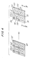
- Step 1 Column bus bars 30 and 32 and the electrodes associated with them, 34a, 34b and 36a, 36b, respectively, are confined on (i.e. applied to) a substrate 40.
- the substrate 40 is preferably made of an electrical insulator such as glass.
- the electrodes are preferably made of a material such as gold, which has high conductivity, although it is opaque.
- the electrodes must be made of a transparent conductor, such as, for example, tin oxide (SnO 2 ).
- the bus bars are conveniently made integrally with the associated electrodes and of the same material, although this is not essential.
- an opaque conductor such as gold can be used for the bus bars even on transmissive displays, provided that the area of the array occupied by the bus bars is relatively small compared to the area occupied by the electrode pairs themselves.
- the method for the confinement of the column bus bars 30 and 32 and associated electrodes on the substrate depends upon the nature of the material they are made of. If they are metallic, the deposition and confinement is preferably done by either deposition, by evaporation or sputtering through a mask having openings (holes) in the shape of the desired pattern held between the substrate and the metal source, or photolithographically, i.e., spreading and patterning a photoresist so that the areas where no metal is desired are left covered with photoresist.
- the metal of the electrodes (and bus bars, if the same material is used for both) is deposited by evaporation or sputtering over the whole substrate. Subsequently, lift-off, i.e., dissolution of the remaining photoresist in a solvent so that it takes with it the overlying metal, leaves on the substrate the desired pattern of the electrodes.
- bus bars and the associated electrodes are made of a conducting and transparent oxide (like tin oxide or indium oxide), then one preferred method to make the pattern of the electrodes is to start with a substrate that already has a coating of the oxide on it. Then the areas where the pattern of the bus bars and the associated electrodes are to be located are protected with a photolithographically confined layer of photoresist. Finally, the unwanted conducting oxide can be dissolved from the unprotected areas with a dilute (1% v/v) hydrogen fluoride solution.
- a conducting and transparent oxide like tin oxide or indium oxide
- Step 2 Pads of insulating material 50 are deposited at points where the row bus bars of the matrix are to cross over the column bars that were deposited in step 1. The purpose of these pads is to prevent shorting of the column and row bus bars at the crossing points.
- the method for the deposition of insulating pads 50 depends on the material used for the pads.
- the pads are preferably of an insulating polymer like polyimide. In this case they are preferably confined photolithographically in the following manner. First, uncross-linked polyimide is spin-coated over the substrate. Then a positive photoresist is spin-coated on top of the polyimide film. Then the photoresist is exposed/developed so that the areas that will define the insulating pads remain covered with photoresist. The unprotected polyimide is dissolved with a base like a dilute solution of sodium hydroxide. Uncross-linked polyimide is commercially available under the trade name PYRALIN® (DuPont).
- the photoresist is removed with acetone leaving polyimide intact to define the pads.
- the polyimide pads then are cured at 400°C for 15 minutes.
- shorts between column and row bus bars at the crossing points caused by pinholes in the insulating layer at the crossing points from dust or other adventitious particles during deposition of these layers are removed by applyina a substantially high voltage across all the rows and columns successively. Shorts then behave like fuses and "blow-up" and disappear, with no apparent change in the matrix appearance or function.
- the pads can also be made of an insulating ceramic like silicon dioxide, or silicon nitride. In this case, the pads are preferably confined in place either by a deposition through the mask, or photolithographically.
- the mask method is the same as the one for the metallic electrode deposition described in step 1 above.
- the photolithographic method involves, first, deposition of the insulating material over the whole surface of the substrate, then protection of the insulating ceramic at the areas where the pads are to be located underneath a layer of photolithographically confined photoresist, and finally removal of the unprotected insulator by exposing the sample to an etching environment.
- an etching environment a dilute solution (1% v/v) of hydrogen fluoride is sufficient to remove silicon dioxide, while a reactive plasma such as a plasma of sulfur hexafluoride or carbon tetrafluoride is necessary to etch silicon nitride.
- a reactive plasma such as a plasma of sulfur hexafluoride or carbon tetrafluoride is necessary to etch silicon nitride.
- the protecting photoresist is removed either by a solvent like acetone, or by exposing the sample to an oxygen plasma.
- Step 3 Row bus bars 60 and 62 and the associated electrodes 60a, 60b and 62a, 62b, respectively, are confined on the substrate so that they cross over the column bus bars at the places where the insulating pads are located, and in such a way that each column electrode has a row electrode associated with it.
- the two electrodes are close to each other, but not in electrical contact.
- the methods to deposit the row bus bars and the associated electrodes are very similar to the methods described above for the deposition and confinement of the column bus bars and the associated electrodes. The only difference is that if the row bus bars or the associated electrodes are to be made of tin oxide, tin oxide has to be deposited/confined over the substrate by some sputtering/photolithographic technique.
- Sputtering materials usually demand annealing after deposition which involves heating the substrate at 400-500°C. This process, therefore, excludes polyimide from being used for making the insulating pads 50, because polyimide films decompose upon heating above 400°C.
- a single pair of electrodes 34a and 60b i.e., one pixel thus constructed is shown in Figure 2.
- the matrix at this stage is ready for the electrochromic materials deposition.
- the entire array except the areas of the two electrodes of each electrode pair 65a, 65b, 65c and 65d and the area of the substrate between the two electrodes is encapsulated with a thin film of an insulating material 70 (such as the material used for the insulating pads of step 2 of Figure 1) as depicted in step 3A of Figure 1A and Figure 3.
- an insulating material 70 such as the material used for the insulating pads of step 2 of Figure 1
- the material of the film must be compatible with contemplated subsequent processing steps. For example, if subsequent steps demand high temperature treatment, polyimide should not be used.
- Step 3A of Figure 1A and Figure 3 depict where film 70 is deposited; however, it is omitted from the rest of Figure 1A for simplicity.
- the purpose of this encapsulating/insulating layer is to prevent any electrochromic material to be deposited electrochemically in a subsequent step from growing on the bus bars.
- Such permanent passivation of any electrode (or bus bar) area not to be covered with an electrochromic material is also advantageous from the standpoint that it makes further photolithographic steps to confine electrodeposited material on the electrodes unnecessary. This also prevents any contact of electrochromic material with photoresist, which contact could be detrimental for the electrochromic material.
- polyaniline coming in contact with positive photoresist like Shiepley's MICROPOSIT® series leads to a permanent greenish coloration of the polyimide film.
- This encapsulation is preferably performed in the same manner as the deposition of insulating pads described in step 2 above.
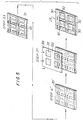
- electrodes 34a' and 60a' of pairs 65a', 65b', 65c' and 65d' have fingers 67 and 68, respectively, which are interdigitated with one another, but not in electrical contact.
- Such interdigitation of the electrodes provides certain advantages, such as maintaining a relatively constant voltage drop along the fingers of the electrodes.
- the row and/or column electrodes and bus bars can be embedded into the surface of the substrate. Embedding the bus bars and electrodes allows thicker bus bars and electrodes to be used, thus increasing electrical conductivity.
- the substrate is first photolithographically etched in the areas where the electrodes and/or bus bars are to be deposited. When the electrodes and/or bus bars are subsequently deposited onto the etched areas as described above, the electrodes and/or bus bars will be at least partially embedded into the surface of the substrate.
- Step 4 and Step 5 Turning again to Figure 1A, row electrodes 60a, 60b and 62a, 62b of each pair are derivatized (i.e. covered) on their outward faces with an electrochromic material 80.
- the column electrodes 34a, 34b and 36a, 36b of each pair are next preferably derivatized with a material 82 which is electrochemically complementary to the electrochromic material on the row electrodes.
- electrochemically complementary is meant that when a bias of sufficient magnitude is applied across the electrodes, one of the materials will undergo reversible oxidation while the other material will undergo reversible reduction to substantially the same extent, without chemically altering the electrolyte (to be described below) or the material of the electrodes themselves.
- both materials 80 and 82 are electrochromic and preferably both materials are complementarily electrochromic in the sense that one changes from a light (colorless or faintly colored) state to a dark (colored) state when oxidized (i.e. upon the removal of electrons) and the other changes from a light state to a dark state when reduced (i.e. upon the addition of electrons).
- both side by side electrochromic material covered electrodes of a pair i.e. one pixel
- the following pairs of complementary electrochromic materials are particularly suitable for use in the present invention: (a) tungsten trioxide (WO 3 ) and polyaniline; (b) W03 and poly 3-methylthiophene (p3MeT); (c) viologen, such as is disclosed, for example, in U.S. Patent No, 4,473,695, and polyvinylferrocene; (d) viologen and poly 3-methylthiophene; (e) WO 3 and anodically grown iridium oxide (AIROF).
- WO 3 tungsten trioxide
- p3MeT poly 3-methylthiophene
- viologen such as is disclosed, for example, in U.S. Patent No, 4,473,695, and polyvinylferrocene
- viologen and poly 3-methylthiophene WO 3 and anodically grown iridium oxide (AIROF).
- the first material in all these pairs turns from light to dark when reduced, that is when it acquires electrons, and the second material of each pair turns from light to dark when oxidized, that is when it releases electrons.
- one material can operate as sink, while the other material can operate simultaneously as a source of reducing or oxidizing equivalents (electrons and holes respectively).
- the preferred way to deposit WO 3 is by sputtering using a WO 3 target in an oxygen/argon (20:80) plasma. Patterning of WO 3 to cover only the column electrode surfaces can be achieved either by deposition through a mask, or by photolithographic protection of the WO 3 at those areas it is going to be preserved, under a photoresist layer.
- the unprotected WO 3 is etched away in a sulfur hexafluoride or a carbon tetrafluoride plasma such as described in Microfabrication of WO 3 -Based Microelectronic Devices, M. O. Schloh, N. Leventis, M. S. Wrighton, J. Appl. Phys. 1989, Vo. 66, P. 965. Finally the protecting photoresist layer over WO 3 is removed either in an oxygen plasma, or by dissolving it with a solvent like acetone.
- the deposition and patterning methods of WO 3 employ severe conditions like the use of plasmas (Ar/O 2 and SF 6 respectively), and a substrate temperature -400 °C during deposition. These conditions exclude the possibility of depositing polyaniline first, because polyaniline is an organic polymer, and as such is unstable at elevated temperatures and in plasma environments. Therefore only after WO 3 has been deposited and patterned as described above, polyaniline is deposited by submerging the entire matrix in an aqueous solution of aniline (-50 mM)/sulfuric acid (0.5 M)/sodium bisulfate (0.5M), and cycling the potential of each row from -0.1 to +0.75 vs. SCE, until the amount of polyaniline electrochemically equivalent to WO 3 has been deposited on the electrodes associated with the row bus bars.
- aniline -50 mM
- 0.5 M sodium bisulfate
- WO 3 is deposited and confined on the column bus bar electrodes first.
- Poly 3-methylthiophene is deposited on the row bus bar electrodes second by submerging the entire matrix in a solution of 3-methylthiophene (-50 mM) in acetonitrile/0.5 M tetrabutylammonium perchlorate, and cycling the potential of each row from 0.0 V to +1.8 V vs. SCE, until the amount of p3MeT electrochemically equivalent to WO 3 has been deposited on the electrodes associated with the row bus bars.
- viologen is deposited by submerging the matrix in an oxygen free aqueous solution containing 0.5 M potassium chloride, 0.5 M dibasic sodium phosphate, and -5 mM of (N,N'-bis[-3-(trimethoxysilyl) propyl]-4,4'-bipyridinium) dibromide, and cycling the potential of each column (or row, as appropriate,) electrode from 0.0 to -0.75 V vs. SCE.
- Polyvinylferrocene is preferably deposited from a 50 mM solution of polyvinylferrocene in methylene chloride by holding the potential of the row (or column) bus bar at +0.6 V vs. SCE, until an electrochemically equivalent amount of polyvinylferrocene has been deposited on the row bus bar electrodes. In this case the conditions for the deposition of each material are completely safe for the other material, so that the deposition sequence is of no importance.
- iridium oxide can be formed by subjecting the iridium film to an oxidizing potential (-+0.5 V vs. SCE) in a dilute sulfuric acid solution.
- the preferred sequence here is to first deposit and photolithographically confine iridium metal over the electrodes associated with the column bus bars, and then to deposit and confine WO 3 over the electrodes associated with the row bus bars. Finally the iridium metal over the column bus bar electrodes will be oxidized anodically by submerging the matrix in a sulfuric acid solution and potentiostating the column bus bars at -+0.5 V vs. SCE.
- the electrochromic material 80 on the row electrode of a given pair is not in contact with the other electrode of the pair or its redox active material 82.
- Such an arrangement will prevent "shorting" of the electrodes of the pair and give the pixel a "memory" such that, once a particular redox state of the materials 80 and 82 on the electrodes is obtained by application of a potential to the pair of electrodes, that state will be reversibly maintained for a relatively long period of time without further application of power, analogously to the charging of a battery.
- the materials can be placed in contact.
- Step 6 An electrolyte 85, preferably a solid electrolyte, is spread on top of the array.
- the electrolyte 85 plays the same role as the electrolytic solution plays in a liquid cell (e.g. sulfuric acid in a lead acid battery).
- the solid electrolyte material is preferably durable and is applied in a thin layer. This eliminates the problem of leakage, and gives the desirable features of an all solid state electrochemical/electrochromic cell.
- Sold electrolyte systems which may be used for the present invention include ⁇ -alumina, and resin gels containing sulfuric acid.
- ⁇ -alumina has the disadvantage that it is ionically conductive only at elevated temperatures, while acidic gels are prone to yield hydrogen evolution at the cathode, with detrimental effects on the ionic conductivity.
- "Aprotic" polymeric solid electrolytes that conduct substantially around room or even lower temperatures are preferred.
- a preferred though non-limiting example is poly ⁇ bis-[methoxyethoxyethoxy]phosphazene ⁇ /lithium triflate.
- the deposition is done preferably by spin-coating a solution of the solid electrolyte in some solvent, and then letting the substrate dry in a controlled atmosphere.
- polyvinylalcohol/phosphoric acid is spread as a dense (viscous) aqueous solution and is allowed to dry at 35 °C in the air. Preferably it is then placed for at least two hours in a water saturated argon atmosphere before the next step.
- Polyethylene oxide/lithium triflate as another example, is preferably spread as a dense solution in anhydrous acetonitrile under dry conditions, and the coated substrate is let to dry under dry argon.
- Step 7 This step comprises a new method to pattern the ion-conductive areas of a solid electrolyte film, to essentially "build" in place ionically insulating border regions between ionically conductive electrolyte areas.
- Each pair of the derivitized electrodes 36a, 60a; 36b, 62a; 34b, 62b or 34a, 60b (i.e. one pixel) is covered with a layer of electrolyte 85, preferably a substantially solid polymer electrolyte such as poly ⁇ bis-[methoxyethoxyethoxy]phosphazene ⁇ /lithium triflate.
- the entire array is covered with the electrolyte as by, for example, spin coating.
- the layer of electrolyte 85 associated with a pair of electrodes includes and is surrounded by a relatively non-conductive border region 90 so that each pair of derivatized electrodes and its associated zone of the layer of electrolyte is a single substantially independent electrochemical cell, relatively unaffected by the redox state of adjacent cells, including those longitudinally connected to a particular row or column bus bar.
- This non-conductive border 90 is depicted in the last figure of Figure lA and in Figure 6. Thus, cross-talk between pixels, even along a single bus bar, is substantially eliminated.
- the preferred method of building the border region is a photolithographic method and is based on electromagnetic radiation induced reduction of the ionic conductivity of the electrolyte.
- the conductivity of poly ⁇ bis-jmethoxyethoxyethoxy]phosphazene ⁇ decreases by crosslinking upon exposure to peroxides, sulfur and radiation as is stated in "Polyphosphazenes: Performance Polymers for Specialty Applications", by H. R. Penton in "Inorganic and Organometallic Polymers", ACS Symposium Series 360, edited by Martel Zeldin, Kenneth J. Wynne, and Harry R. Allcock.
- the electromagnetic radiation preferably gamma, X-rays or ultraviolet radiation, is shown onto the electrolyte layer through mask 100.
- the dark areas 101 of mask 100 prevent exposure of the electrolyte in the regions 92 covering the electrode pairs so that these regions remain ionically conductive.
- Electromagnetic radiation goes through light areas 102 of mask 100 to expose the underlying electrolyte layer in the border regions 90 surrounding the electrode pairs. The radiation induces cross-linking the polymeric backbone of the solid electrolyte in regions 90, decreasing its ionic conductivity in the exposed regions.
- Another preferred embodiment of this method is to mix into the solid electrolyte a UV-sensitive monomer or oligomer, which upon exposure to UV-light induces crosslinking of the monomer or oligomer with itself or the polymeric backbone.
- Possible crosslinkers for the case of poly ⁇ bis-[methoxyethoxyethoxy]photophazene ⁇ include illustratively, divinylbenzene or vinyl acrylate and similar compounds that are able after photoexitation, to connect the polyphosphazene chains in a three dimensional network. It is believed that this is accomplished by attacking the alternating double bonds of the polyphosphazene polymeric backbone, following a radical type mechanism.
- the unpolymerized crosslinker can be removed either by applying vacuum or by heating the substrate, or it can be washed away using a solvent system that leaves the rest of the materials on the matrix intact. Which method is preferably followed depends on the crosslinker, and the materials on the array.
- the crosslinker can also be left on the array permanently as long as it is electrochemically inert with the range of voltages applied during use of the array to address the electrochromic materials in the electrode pairs of the array.
- the array is preferably encapsulated (i.e., covered) with a front near-UV filter, such as common glass.
- a front near-UV filter such as common glass.
- Another illustrative but non-limiting example of the method for patterning the conducting regions of a solid electrolyte is to photorelease a substance that reduces the mobility of the current supporting ions in the exposed areas.
- incorporation of a metal complex that can photorelease water in the polyethylene oxide/lithium triflate solid electrolyte system can render the electrolyte system ionically non-conductive by photosolvating the lithium ions upon exposure to UV-light.
- a substance that can photorelease a base e.g. [Co(NH 3 ) 6 )Cl 3 , [Ru(NH 3 ) 6 )Cl 3 , [Co(NH 3 ) 5 Cl]Cl 2 etc.
- a solid electrolyte system like polyvinylalcohol/phosphoric acid.
- Disposing both electrodes of each pair side by side on one substrate makes alignment of the column and row electrodes very easy by conventional microfabrication techniques.
- the lower limits in feature size then can be as low as the limits the standard VLSI technology can achieve, that is less than 1 micron.
- This miniaturization also decreases the RC time constant for the charging of the electrodes of each pixel which in turn increases the response time of each pixel and of the matrix as a whole. Feature size of less than about 75 microns is believed to give the best combination of ease of fabrication and good operation without preferential coloration.
- the miniaturization increases the resolution of electrochromic screens, and reconfigurable projection devices become easy to manufacture.
- Minimum feature size for the two dimensional arrays of electrochemical cell as are described herein is defined as the distance between the two electrodes of each electrode pair.
- Pixel size as small as two microns across is possible with arrays constructed in accordance with the present invention.
- pixel size should be between about 2 microns and 250 microns across for good resolution. Pixel size between 2 microns and 75 microns is preferred, as being reasonably easy to fabricate, but much smaller than normal human visual acuity.
- the individual pixel may be of any size, including several inches across, but the width of the fingers is preferably greater than about 2 microns and less than about 50 microns for best performance and minimization of preferential coloration of portions of the electrodes.
- the array may have any number of pixels.
- the array of the present invention having electrodes of each pair arranged side by side and on the same substrate described above with respect to Figures 1, 2, 2A, 3, 3A and 6 is also of great advantage applied to emissive arrays such as those utilizing electroluminescent substances and those utilizing electrochemiluminescent materials.
- the preferred feature size and pixel size of these arrays are the same as for the electrochromic displays described above.
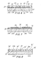
- step 3A' of Figure 4 it is desirable with electroluminescents to have the electroluminescent substance insulated from the electrodes themselves. Therefore, the entire array, including the electrodes, is preferably covered with insulating film 70' in step 3A'. This step can be omitted, if desired.
- each pair of electrodes of the array is covered with a layer of an electroluminescent substance 95 such as, for example, manganese doped zinc sulfide.
- an electroluminescent substance 95 such as, for example, manganese doped zinc sulfide.
- the electroluminescent covering over each electrode pair is isolated from the electroluminescent covering over adjacent electrode pairs.
- the electroluminescent material over and between the electrodes of a pair will luminesce upon application of a bias of sufficient magnitude between the row and the column at the intersection of the electrode pair.
- the preferred embodiment of the array is one where the two electrodes of each electrode pair are interdigitated, as depicted in Figures 2A and 3A. This is because light will be emitted from all the interfinger areas, thus giving increased luminance density compared to the non-interdigitated electrode pair configuration.
- the configuration of the present invention will approach the luminosity of the conventional sandwich structure, while having higher resolution and being easier to fabricate.
- Electrochemiluminescent materials are substances A, which have stable oxidized (A + ) and reduced (A - ) forms, both of which are reversibly and electrochemically accessible, that can react with each other in an annihilation fashion to yield substance A, some of which are in an electronically excited state (A*) that can relax to the ground state (A) by emission of one photon of light.
- the oxidized and reduced forms of A can be produced electrochemically, i.e., preferably via fast cycling of the potential of a pair of electrodes immersed in a solution of A. Thus, no net chemical change happens on the bulk of the electrolyte since A is regenerated.
- a + and A - can be induced with different electrodes where a bias large enough has been applied.
- both reactions (1) and (2) take place simultaneously and to the same extent if electrolyte and electrode are inert, and in such a way that reaction (1) happens on the negative electrode and reaction (2) on the positive electrode.
- a - and A + diffuse away from their generation sources (i.e. the electrodes) and eventually meet each other somewhere between the two electrodes.
- reactions (3) and (4) take place with generation of light.
- substance A is soluble in the solid electrolyte employed.
- Combinations of solid electrolyte/electrochemiluminescent substances useful in the present invention include:
- an electrochemiluminescent array and an array so constructed are depicted.
- the array of side by side row and column electrodes is preferably built as described with respect to steps 1 through 3 of Figure 1 preferably including step 3A of Figure 5 where the entire array except for the electrodes themselves and the interelectrode space is covered with an insulating film 70, in the same manner as described with respect to the Figure 1A embodiment.
- the electrochemiluminescent substance is mixed into the electrolyte itself, rather than being coated onto the electrodes, the steps 4 and 5 of Figure 1A having to do with coating the electrodes are not required.
- Step 6" is preferably accomplished in the same manner as Step 6 of Figure 1A, the only exception being that the electrochemiluminescent substance is mixed into the electrolyte 85', preferably before the electrolyte 85' is applied.
- the electrochemiluminescent substance must be compatible with (i.e. nonreactive with) the monomer or oligomer or other photosensitive substances.
- the preferred embodiment of an electrochemiluminescent display in accordance with the present invention has side by side electrode pairs with the photoconductivity patterned solid electrolyte as described above with respect to the electrochromic embodiment of Figure 1A.
- the masking and selective exposure of the electrolyte to U.V. radiation depicted in step 7" is accomplished in the same manner as described with respect to step 7 of Figure 1A.
- the active component i.e., the electrochemiluminescent compound
- the active component may also be incorporated at the end, after the array has been covered with the solid electrolyte film.
- the conductivity-patterned solid electrolyte covered array is exposed to vapors of the electrochemiluminescent substance, such as anthracene, which will diffuse into the electrolyte.
- the integrated configuration of electrode pairs as depicted in Figures 2A and 3A is preferable because it provides more interelectrode spaces where the A + and A - can meet and annihilate each other, provides less distance for A + and A - to travel (by diffusion) before they meet, which makes response of the matrix faster, and permits all electrodes to be made of metal and on the same substrate for ease of fabrication and improved conductivity.
- Another embodiment of the present invention as a luminescent display is a configuration in which the array is covered with a patterned solid electrolyte layer in which a compound has been dissolved that can be triggered by UV-light to luminesce only from one of its redox states.
- Compounds having this property are anthraquinone or other substituted anthraquinones which upon reduction yield 9, 10-dihydroanthracene which luminesces green light upon UV-light excitation.
- the solid electrolyte can be polyvinylalcohol/phosphoric acid while the counter electrode can be derivatized with polyvinylferrocene in a complementary counterelectrode fashion.
- the construction and operation of such an array is the same as for the electrochromic array described in Figures 1, 2, 2A, 3, 3A and 6.
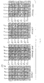
- an electrochromic array constructed in accordance with the present invention to display information will now be described.
- an array 25 of the type described in Figures 1A and 3 is used, including pixels with two complementary electrochromic materials, under a layer of a solid electrolyte, the functionality of which has been patterned in accordance with the present invention to crease separate blocks of ion-conductive electrolyte for each pair of electrodes surrounded by substantially non-conductive border regions.
- the following describes, by way of example, how this array can be electrically addressed in order to display the number "2", and how this displayed informaticn can be changed to something else, for example, to the number "4".
- the array used in this example is of the 5x7 type that is customarily used for the display of alphanumeric information.
- the example is not intended to be limiting either on the size of the matrix or the kind of information to be displayed.
- the same addressing concepts can be used to display pictures.
- the 5x7 array of this example preferably accomplishes this task in the following four steps:
- the array 25 is powered by a power supply (not shown) through a computer controlled series of switches (not shown) that can connect any row or column bus bar (from now on called simply “row” or “column") to either the "+” or the "-" terminal of the power supply, or disconnect any row or column from any active control when desired.
- a pixel is colorless when its column bus bar is at “-”, and its row bus bar is at "+”; and a pixel is colored when its column bus bar is at "+”, and its row bus bar at "-”.
- the potential difference between the "+" and "-" terminals for the coloration reaction to be affected must be at least equal to the threshold voltage for the coloration reaction, which is approximately equal to the difference in the formal redox potentials of the two redox active materials on the two electrodes of each pixel. It should also be noted that a pixel retains its colored state when at least one of its connections to the power supply is removed while the pixel is at the colored state under consideration due to the memory effect of the electrochromic materials.
- Step 1 This step clears the matrix, and prepares it to accept a new frame. In the present example this is accomplished by connecting simultaneously all columns to "-" and all rows to "+".
- Step 2 Display "frame one". This is accomplished by writing one line (i.e. a single row) at a time by coloring the appropriate pixels of each line, in a line-at-a-time pace. It is necessary to write only one line at a time because if two or more rows are addressed simultaneously, additional unwanted pixels may color.
- Each row is addressed by connecting it to "-". While each row is being addressed, the columns are held either at "+” if the pixel at the intersection of the particular row and the corresponding column is to be colored, or if this pixel has to remain colorless, the corresponding column can be either let to float (i.e. be unconnected to either "+” or "-”), or it can be connected to "-".
- Step 3 To change the displayed image, the entire array is again reset as described in step 1.
- Step 4 Display step 4 in a line-at-a-time fashion in the manner described above for step 2.
- steps 3 and 4 above can be combined into a single step. That is, when it is desired to change the displayed "2" to a "4", only those pixels whose colored/uncolored states are required to be changed are changed by reversing the polarity of the voltage applied at each required address location in the line-by-line manner described in step 2 above.
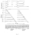
- connection of the columns or the rows to the "+" or. the "-" terminals of the power supply can be thought of as a train of synchronized pulses (positive or negative) directed simultaneously to the columns and the rows of the matrix.
- Figures 10 and 11 demonstrate such trains of pulses that can accomplish the task as described in Figure 9. It should be noted that the duration of the negative pulse at each row is a little shorter than the pulse to the columns. This means that before control is transferred to the next row, the present row is first disconnected and only then the signal configuration on the columns is changed in order to write the next row.
- Figure 10 demonstrates the train of pulses where the columns of unselected pixels are held negative.
- Figure 11 depicts the train of pulses where the columns of unselected pixels are allowed to float.
- each row after it has been addressed may be connected to positive. However, in this illustrative scheme, this row will be erased and no advantage will be capitalized from the memory effect of electrochromic materials.
- a reconfigurable projection device that is, a transparent "slide" which may be electrically reconfigured to display different images or information when light is shone through it may be constructed using electrochromic arrays in accordance with the present invention. By appropriate selection of electrochromic materials employed, or an overlay of colored materials, a color display may be constructed.
- a reconfigurable projection device in accordance with the present invention may include a single array 26 or two or more laminated layers of such arrays.
- the present invention may be used as a reconfigurable photomask for the microfabrication of integrated circuits.
- a reconfigurable photomask could replace the multiplicity of photomasks presently necessary for making an integrated circuit by only one mask that can assume many configurations at will by matrix addressing.
- Such an application takes advantage of the fact that very small size pixels, in the range of a few microns, can be fabricated using arrays in accordance with the present invention. It is preferred that these pixels be as small as possible for best resolution, but pixels as large as 250 microns or greater may be employed with suitable reduction optics.
- a reconfigurable photomask for the purpose stated above should have the ability to selectively color/bleach each pixel of the entire surface of a matrix, and particularly the area between the pixels, although it is not necessary to create the entire pattern at one time. That is, a reconfigurable photomask in accordance with the present invention may selectively color/bleach as little as a single pixel at a time. This can be done repeatedly, pixel by pixel, until the desired pattern to be exposed on the substrate of the integrated circuit (corresponding to one photomasking step) is completed, provided that the aggregate of all pixels of the area of the photomask gives complete control over the trasmissivity or opacity of the area on a pixel/by/pixel basis. This process is repeated for subsequent manufacturing steps requiring a different pattern.
- any additional exposure time is more than compensated for by the savings in time and manufacturing steps made possible by use of a single, electrically reconfigurable photomask instead of several steps required to make and use conventional multiple photomasks.
- a transparent light modulating array I such as, for example, the electrochromic array depicted in cross-section in Figure 6, is laminated on top of a light emitting display array II such as, for example, the electroluminescent array depicted in cross-section in Figure 4 by means of laminating compound 200, which may be an epoxy, for instance.
- laminating compound 200 which may be an epoxy, for instance.
- the electrodes of array I must be transparent.
- this combined display is the same as the construction and operation of either array alone, except that overlying pixels of the two arrays are addressed simultaneously. This, if it is desired that a pixel be dark, the electrochromic pixel will be colored and the corresponding electroluminescent pixel below it will be left in its non-light emitting state.
- an electrochromic pixel on array I comprised of a pair of electrodes 36b and 62a derivatized with complementary electrochromic coverings 82 and 80, respectively, is depicted as uncolored.
- the electroluminescent material 95 of the pixel in array II directly underneath the colored pixel of array I is left dark, while the electroluminescent material 95 of the pixel in array II directly underneath the uncolored pixel of array I is turned "on" so that it emits light.
- This configuration essentially multiplies the contrast from each layer, resulting in an overall display having higher contrast and sharper resolution than would be possible with either layer alone.
- a light modulating array utilizing liquid crystals as the light modulating material may also be employed.
- liquid crystals could be employed with polarizing filters instead of electrochromics for use as a reconfigurable photomask, using the same configuration and alignment of electrodes.
- multi-layer laminated assemblies can also be constructed fully or partially offset from each other and with electrochromics having different color change states, for an application where the final assembly is going to be used as a reconfigurable projection slide.
Abstract
Description


Claims (10)
- An electrochromic display pixel comprising a substrate (40) and a pair of electrodes (65a, 65b), at least one of said electrodes being coated on its face with a first chemical substance (80) which is electrochromic, characterised in that said pair of electrodes are mounted face up and side by side on one side of said substrate and in close proximity to each other, and said display pixel further comprises a layer of ionically conductive electrolyte (65) over said electrode pair (65a, 65b) to complete an electrochemical cell so that when a bias is imposed between the electrodes of said pair said first chemical substance (80) changes its spectral absorption characteristics a relatively non-conductive border region (90) surrounding said electrode pair, and a transparent cover having a substantially non-conductive face in contact with said electrolyte layer.
- The display pixel defined in Claim 1, wherein said first chemical substance material (80) is confined on one of said electrodes (34a, 34b) and the other electrode (60a, 60b) of said pair is coated with a second chemical substance (82).
- The display pixel defined in Claim 2, wherein said second chemical substance (82) is electrochromically complementary to said first chemical substance.
- The display pixel defined in Claim 3, wherein said first chemical substance (80) is viologen and said second chemical substance is polyvinylferrocene.
- The display pixel defined in any preceding claim, wherein said electrodes of said pair (67, 68) interdigitate with each other.
- An electroluminescent display pixel comprising a substrate (40) and a pair of electrodes (65a, 65b) characterised in that said pair of electrodes is mounted face up and side by side on one side of said substrate (40) and in close proximity to each other, and said display pixel further comprises an electroluminescent chemical substance (95) over each electrode pair (65a, 65b) and the space between them to form a bridge between them so that when a bias is imposed between the electrodes of said pair (65a, 65b) said electroluminescent chemical substance emits light.
- The display pixel defined in Claim 6, wherein said electroluminescent chemical substance is an electrochemiluminescent chemical substance comprised in an electrolyte.
- An electrochromic display comprising an array of matrix addressable pairs of electrodes, said array comprising:a. a substrate (40)b. a plurality of substantially parallel and spaced apart electronically conductive means defining columns of bus bars (30,32) mounted on one side of said substrate (40), each of said column bus bars (30,32) being electrically separate from the other column bus bars (30,32) so that each is independently addressable by electrical biasing means;c. a plurality of column electrode means (34a, 34b, 36a, 36b) mounted face up on said one side of said substrate and spaced at intervals along each of said column bus bars (30,32);d. a plurality of substantially parallel and spaced apart electronically conductive means defining row bus bars (60,62) on said one side of said substrate (40), said row bus bars (60,62) crossing but being electrically insulated from said column bus bars (30,32), each of said row bus bars (60,62) being electrically separate from the other row bus bars (60,62) so that each of said row bus bars (60,62) is independently addressable by electrical biasing means;e. a plurality of row electrode means (60a, 60b, 62a, 62b) mounted face up on said one side of said substrate (40) and spaced at intervals along each row bus bar (60,62), each of said row electrodes being positioned to have a column electrode in close proximity to and side by side therewith to define an electrode pair (65a, 65b, 65c, 65d), at least one of said electrodes of each said pair being coated on its face with a first electrochromic material (80); characterised byf. a layer of ionically conductive electrolyte (85) over said pairs of electrodes, to complete an electrochemical cell, said layer of electrolyte being separated by relatively non-conductive border regions into a plurality of zones, each of said zones being associated with one of said pair of electrodes; andg. a transparent cover having a substantially non-conductive face in contact with said electrolyte layer.
- The display defined in Claim 8, wherein the row electrode (68) of each pair interdigitates with its associated column electrode (67).
- A display as claimed in Claim 8 or 9 wherein said display is multi-layer laminated having first and second matrix addressable arrays.
Applications Claiming Priority (3)
| Application Number | Priority Date | Filing Date | Title |
|---|---|---|---|
| US07/485,379 US5189549A (en) | 1990-02-26 | 1990-02-26 | Electrochromic, electroluminescent and electrochemiluminescent displays |
| US485379 | 1990-02-26 | ||
| PCT/US1991/001322 WO1991013381A1 (en) | 1990-02-26 | 1991-02-26 | Electrochromic, electroluminescent and electrochemiluminescent displays |
Publications (3)
| Publication Number | Publication Date |
|---|---|
| EP0531298A1 EP0531298A1 (en) | 1993-03-17 |
| EP0531298A4 EP0531298A4 (en) | 1994-03-09 |
| EP0531298B1 true EP0531298B1 (en) | 1998-01-28 |
Family
ID=23927928
Family Applications (1)
| Application Number | Title | Priority Date | Filing Date |
|---|---|---|---|
| EP91905939A Expired - Lifetime EP0531298B1 (en) | 1990-02-26 | 1991-02-26 | Electrochromic, electroluminescent and electrochemiluminescent displays |
Country Status (12)
| Country | Link |
|---|---|
| US (2) | US5189549A (en) |
| EP (1) | EP0531298B1 (en) |
| AT (1) | ATE162893T1 (en) |
| AU (1) | AU7475691A (en) |
| CA (1) | CA2037014C (en) |
| DE (1) | DE69128830T2 (en) |
| DK (1) | DK0531298T3 (en) |
| ES (1) | ES2114886T3 (en) |
| GR (1) | GR3026735T3 (en) |
| IL (1) | IL97335A (en) |
| WO (1) | WO1991013381A1 (en) |
| ZA (1) | ZA911266B (en) |
Families Citing this family (117)
| Publication number | Priority date | Publication date | Assignee | Title |
|---|---|---|---|---|
| US5280381A (en) * | 1992-07-27 | 1994-01-18 | Ford Motor Company | Process for preparing a solid polymeric fast ion conducting layer for an electrochromic device |
| US5652067A (en) * | 1992-09-10 | 1997-07-29 | Toppan Printing Co., Ltd. | Organic electroluminescent device |
| US5754329A (en) * | 1992-12-22 | 1998-05-19 | Monsanto Company | Electrochromic display laminates |
| US5413739A (en) * | 1992-12-22 | 1995-05-09 | Coleman; James P. | Electrochromic materials and displays |
| US5682043A (en) * | 1994-06-28 | 1997-10-28 | Uniax Corporation | Electrochemical light-emitting devices |
| US5780160A (en) * | 1994-10-26 | 1998-07-14 | Donnelly Corporation | Electrochromic devices with improved processability and methods of preparing the same |
| US5729379A (en) * | 1994-10-26 | 1998-03-17 | Donnelly Corporation | Electrochromic devices |
| JP3241251B2 (en) * | 1994-12-16 | 2001-12-25 | キヤノン株式会社 | Method of manufacturing electron-emitting device and method of manufacturing electron source substrate |
| US6673533B1 (en) | 1995-03-10 | 2004-01-06 | Meso Scale Technologies, Llc. | Multi-array multi-specific electrochemiluminescence testing |
| US6207369B1 (en) | 1995-03-10 | 2001-03-27 | Meso Scale Technologies, Llc | Multi-array, multi-specific electrochemiluminescence testing |
| AU720625B2 (en) * | 1995-03-10 | 2000-06-08 | Meso Scale Technologies, Llc | Multi-array, multi-specific electrochemiluminescence testing |
| US6140045A (en) | 1995-03-10 | 2000-10-31 | Meso Scale Technologies | Multi-array, multi-specific electrochemiluminescence testing |
| WO1996036959A2 (en) * | 1995-05-19 | 1996-11-21 | Philips Electronics N.V. | Display device |
| AU5799596A (en) * | 1995-05-19 | 1996-11-29 | Uniax Corporation | Electrochemical light-emitting devices |
| US5895717A (en) * | 1995-11-08 | 1999-04-20 | Uniax Corporation | Electrochemical light-emitting devices |
| US5677546A (en) * | 1995-05-19 | 1997-10-14 | Uniax Corporation | Polymer light-emitting electrochemical cells in surface cell configuration |
| WO1996041233A1 (en) * | 1995-06-07 | 1996-12-19 | Monsanto Company | Device and method for light modulation |
| US5876633A (en) * | 1995-12-26 | 1999-03-02 | Monsanto Company | Electrochromic metal oxides |
| US5891511A (en) * | 1995-12-26 | 1999-04-06 | Monsanto Company | Addition of color to electrochromic displays |
| CA2241286A1 (en) * | 1995-12-26 | 1997-07-03 | Monsanto Company | Electrochromic tin oxide |
| JP2734442B2 (en) * | 1996-01-30 | 1998-03-30 | 日本電気株式会社 | Thin film EL device and method of manufacturing the same |
| FR2746934B1 (en) * | 1996-03-27 | 1998-05-07 | Saint Gobain Vitrage | ELECTROCHEMICAL DEVICE |
| EP0898730A4 (en) | 1996-04-10 | 2001-09-26 | Donnelly Corp | Electrochromic devices |
| US6958245B2 (en) | 1996-04-25 | 2005-10-25 | Bioarray Solutions Ltd. | Array cytometry |
| US7041510B2 (en) | 1996-04-25 | 2006-05-09 | Bioarray Solutions Ltd. | System and method for programmable illumination pattern generation |
| CA2255599C (en) | 1996-04-25 | 2006-09-05 | Bioarray Solutions, Llc | Light-controlled electrokinetic assembly of particles near surfaces |
| US6387707B1 (en) | 1996-04-25 | 2002-05-14 | Bioarray Solutions | Array Cytometry |
| US7144119B2 (en) * | 1996-04-25 | 2006-12-05 | Bioarray Solutions Ltd. | System and method for programmable illumination pattern generation |
| US5989752A (en) * | 1996-05-29 | 1999-11-23 | Chiu; Tzu-Yin | Reconfigurable mask |
| WO1998003042A1 (en) * | 1996-07-16 | 1998-01-22 | Philips Electronics N.V. | Organic electroluminescent device |
| FR2758431A1 (en) * | 1997-01-10 | 1998-07-17 | Commissariat Energie Atomique | THIN-LAYER ELECTROLUMINESCENT DISPLAY DEVICE WITH ALTERNATIVE EXCITATION AND ITS EMBODIMENT PROCESS |
| US20030027126A1 (en) | 1997-03-14 | 2003-02-06 | Walt David R. | Methods for detecting target analytes and enzymatic reactions |
| US7622294B2 (en) | 1997-03-14 | 2009-11-24 | Trustees Of Tufts College | Methods for detecting target analytes and enzymatic reactions |
| US5952778A (en) * | 1997-03-18 | 1999-09-14 | International Business Machines Corporation | Encapsulated organic light emitting device |
| US5877888A (en) * | 1997-06-10 | 1999-03-02 | Monsanto Company | Single and double sided electrochromic displays |
| AU7958398A (en) * | 1997-06-10 | 1998-12-30 | Monsanto Company | Switchable images with fine detail |
| JPH11121178A (en) * | 1997-10-14 | 1999-04-30 | Matsushita Electric Ind Co Ltd | Organic electroluminescent element and its manufacture |
| US6455873B1 (en) * | 1997-12-03 | 2002-09-24 | State Of Oregon Acting By And Through The State Board Of Higher Education On Behalf Of The University Of Oregon | Devices having a semiconductor/conducting polymer interface |
| US6111356A (en) * | 1998-04-13 | 2000-08-29 | Agilent Technologies, Inc. | Method for fabricating pixelated polymer organic light emitting devices |
| US6200531B1 (en) * | 1998-05-11 | 2001-03-13 | Igen International, Inc. | Apparatus for carrying out electrochemiluminescence test measurements |
| KR100267964B1 (en) * | 1998-07-20 | 2000-10-16 | 구자홍 | Organic electroluminescent display panel and method for fabricating the same |
| JP2000040591A (en) * | 1998-07-21 | 2000-02-08 | Sony Corp | Organic electroluminescence element |
| JP3737889B2 (en) * | 1998-08-21 | 2006-01-25 | パイオニア株式会社 | Light emitting display device and driving method |
| US7141436B2 (en) * | 1999-11-03 | 2006-11-28 | Science And Technology Corp. | Immunoassay and reagents and kits for performing the same |
| TW421285U (en) * | 2000-02-03 | 2001-02-01 | Ritek Corp | Colorful long-life luminescence plate |
| JP2001267578A (en) * | 2000-03-17 | 2001-09-28 | Sony Corp | Thin-film semiconductor device, and method for manufacturing the same |
| US6500387B1 (en) * | 2000-05-19 | 2002-12-31 | Nukuest, Inc. | Air actinism chamber apparatus and method |
| US9709559B2 (en) | 2000-06-21 | 2017-07-18 | Bioarray Solutions, Ltd. | Multianalyte molecular analysis using application-specific random particle arrays |
| DE60117556T2 (en) | 2000-06-21 | 2006-11-02 | Bioarray Solutions Ltd. | MULTI-ANALYTIC MOLECULAR ANALYSIS THROUGH THE USE OF APPLICATION SPECIFIC RAPID PARTICLE ARRAYS |
| US7057704B2 (en) * | 2000-09-17 | 2006-06-06 | Bioarray Solutions Ltd. | System and method for programmable illumination pattern generation |
| US20030045005A1 (en) * | 2000-10-17 | 2003-03-06 | Michael Seul | Light-controlled electrokinetic assembly of particles near surfaces |
| GB0103765D0 (en) * | 2001-02-15 | 2001-04-04 | Affitech As | Assay |
| DE60226221T2 (en) | 2001-03-07 | 2009-05-14 | Acreo Ab | ELECTROCHEMICAL PIXEL EQUIPMENT |
| FR2821937B1 (en) * | 2001-03-07 | 2003-06-06 | Saint Gobain | ELECTRICALLY CONTROLLABLE DEVICE WITH VARIABLE OPTICAL AND / OR ENERGY PROPERTIES |
| JP4133336B2 (en) | 2001-03-07 | 2008-08-13 | アクレオ アーベー | Electrochromic devices |
| WO2002075441A2 (en) | 2001-03-19 | 2002-09-26 | Dow Global Technologies Inc. | Electrochromic display device and compositions useful in making such devices |
| JP2002289347A (en) * | 2001-03-27 | 2002-10-04 | Sanyo Electric Co Ltd | Electroluminescence display device, its manufacturing method, covering mask and its manufacturing method |
| WO2002079868A1 (en) | 2001-03-30 | 2002-10-10 | Sony Corporation | Display unit and driving method therefor |
| JP2003017264A (en) * | 2001-04-27 | 2003-01-17 | Canon Inc | Electroluminescent element and image display device |
| US7262063B2 (en) | 2001-06-21 | 2007-08-28 | Bio Array Solutions, Ltd. | Directed assembly of functional heterostructures |
| JP3682584B2 (en) * | 2001-08-06 | 2005-08-10 | ソニー株式会社 | Method for mounting light emitting element and method for manufacturing image display device |
| US6791739B2 (en) * | 2001-08-08 | 2004-09-14 | Eastman Kodak Company | Electro-optic despeckling modulator and method of use |
| KR100444498B1 (en) * | 2001-09-21 | 2004-08-16 | 엘지전자 주식회사 | Hybrid electro-luminescence panel |
| NZ532947A (en) | 2001-10-15 | 2006-01-27 | Bioarray Solutions Ltd | Multiplexed analysis of polymorphic loci by concurrent interrogation and enzyme-mediated detection |
| JP4532908B2 (en) * | 2002-03-07 | 2010-08-25 | アクレオ アーベー | Electrochemical devices |
| CN1304897C (en) * | 2002-03-07 | 2007-03-14 | 阿克里奥公司 | Electrochemical device |
| US6744549B2 (en) * | 2002-03-19 | 2004-06-01 | Dow Global Technologies Inc. | Electrochromic display device |
| JP3951950B2 (en) * | 2002-05-31 | 2007-08-01 | ソニー株式会社 | Driving method of display device |
| US7553448B2 (en) * | 2002-06-20 | 2009-06-30 | Bioveris Corporation | Electrochemiluminescence flow cell and flow cell components |
| DE60302360T2 (en) * | 2002-06-24 | 2006-08-03 | Koninklijke Philips Electronics N.V. | ELECTROCHROME DISPLAY PANEL WITH ELECTRODES FOR ADJUSTING THE TRANSMITTER |
| ATE341018T1 (en) * | 2002-08-15 | 2006-10-15 | Koninkl Philips Electronics Nv | COLOR ELECTROCHROMIC DISPLAY WITH SUPPLIED ELECTROCHROMIC LAYERS |
| US7000870B2 (en) * | 2002-11-07 | 2006-02-21 | Aerion Corporation | Laminar flow wing for transonic cruise |
| AU2003298655A1 (en) | 2002-11-15 | 2004-06-15 | Bioarray Solutions, Ltd. | Analysis, secure access to, and transmission of array images |
| EP1708016B1 (en) * | 2003-01-31 | 2009-03-18 | Ntera Limited | Electrochromic display device and method of making such a device |
| TW583895B (en) * | 2003-03-31 | 2004-04-11 | Ritdisplay Corp | OEL device |
| WO2004112436A1 (en) * | 2003-06-13 | 2004-12-23 | Fuji Electric Holdings Co., Ltd. | Organic el display and method for producing the same |
| JP2005049770A (en) * | 2003-07-31 | 2005-02-24 | Sanyo Electric Co Ltd | Electrochromic display device |
| WO2005012993A1 (en) * | 2003-07-31 | 2005-02-10 | Sanyo Electric Co., Ltd. | Electrochromic display |
| WO2005029163A1 (en) | 2003-09-17 | 2005-03-31 | Segan Industries, Inc. | Flash imaging devices, methods for making and using the same |
| US7927796B2 (en) | 2003-09-18 | 2011-04-19 | Bioarray Solutions, Ltd. | Number coding for identification of subtypes of coded types of solid phase carriers |
| CN1882699A (en) | 2003-09-22 | 2006-12-20 | 佰尔瑞溶液有限公司 | Surface immobilized polyelectrolyte with multiple functional groups capable of covalently bonding to biomolecules |
| US7563569B2 (en) | 2003-10-28 | 2009-07-21 | Michael Seul | Optimization of gene expression analysis using immobilized capture probes |
| ES2533876T3 (en) | 2003-10-29 | 2015-04-15 | Bioarray Solutions Ltd | Multiplexed nucleic acid analysis by double stranded DNA fragmentation |
| JP4138629B2 (en) * | 2003-11-06 | 2008-08-27 | 株式会社東芝 | Surface emitting semiconductor device and manufacturing method thereof |
| TWM265641U (en) * | 2004-06-09 | 2005-05-21 | Rilite Corportation | Double shielded electroluminescent panel |
| US7848889B2 (en) | 2004-08-02 | 2010-12-07 | Bioarray Solutions, Ltd. | Automated analysis of multiplexed probe-target interaction patterns: pattern matching and allele identification |
| GB2419182B (en) * | 2004-10-13 | 2009-06-03 | Basic Holdings | Apparatus for producing an optical effect or for simulating fires and simulated fireplaces including such apparatus |
| WO2006051050A1 (en) * | 2004-11-10 | 2006-05-18 | Siemens Aktiengesellschaft | Electrochromic passive-matrix display comprising an electrolyte that can be structured |
| EP1836495A2 (en) * | 2004-11-17 | 2007-09-26 | BioVeris Corporation | Electrochemiluminescent assay |
| US20060275841A1 (en) * | 2004-12-20 | 2006-12-07 | Martin Blankfard | Assay method and apparatus with reduced sample matrix effects |
| US20060163540A1 (en) * | 2005-01-27 | 2006-07-27 | Chien-Hsin Yang | Solid status electro-chromic device process using conductive polymer nano material |
| WO2006084081A2 (en) * | 2005-02-04 | 2006-08-10 | Appleton Coated, Llc | Display with self-illuminatable image and method for making the display substrate and for making the image |
| US7372609B2 (en) * | 2005-03-16 | 2008-05-13 | Gentex Corporation | Nanocrystalline metal oxide films and associated devices comprising the same |
| US8486629B2 (en) | 2005-06-01 | 2013-07-16 | Bioarray Solutions, Ltd. | Creation of functionalized microparticle libraries by oligonucleotide ligation or elongation |
| KR101311815B1 (en) | 2005-06-03 | 2013-10-22 | 보드 오브 리전츠 오브 더 유니버시티 오브 텍사스 시스템 | Electrochemistry and electrogenerated chemiluminescence with a single faradaic electrode |
| WO2007002580A2 (en) * | 2005-06-23 | 2007-01-04 | Bioveris Corporation | Diagnostic as say system with multi -well reagent container |
| JP2007095488A (en) * | 2005-09-29 | 2007-04-12 | Toshiba Corp | Light emitting element and method of manufacturing same |
| US7372216B2 (en) * | 2006-04-03 | 2008-05-13 | Ceelite Llc | Constant brightness control for electro-luminescent lamp |
| US7961375B2 (en) * | 2008-06-25 | 2011-06-14 | Soladigm, Inc. | Multi-cell solid-state electrochromic device |
| US20100046198A1 (en) * | 2008-08-21 | 2010-02-25 | Night Moves, Llc | Flexible Backlit Display |
| JP2012516033A (en) * | 2009-01-21 | 2012-07-12 | ルナベイション・エービー | Luminescent electrochemical cells and systems, their use and methods for their operation |
| KR20110005097A (en) * | 2009-07-09 | 2011-01-17 | 삼성전자주식회사 | Display panel, display driving apparatus, display apparatus and electrode arranging method |
| EP2395572A1 (en) * | 2010-06-10 | 2011-12-14 | Bayer MaterialScience AG | Layer construction comprising electronic components |
| JP2012027352A (en) * | 2010-07-27 | 2012-02-09 | Funai Electric Advanced Applied Technology Research Institute Inc | Electrochromic display device |
| KR101231991B1 (en) * | 2011-02-18 | 2013-02-08 | 경성대학교 산학협력단 | The structure of a electrochemiluminesence cell |
| US20130222877A1 (en) | 2012-02-28 | 2013-08-29 | Sage Electrochromics, Inc. | Multi-zone electrochromic devices |
| TWI505002B (en) * | 2013-02-05 | 2015-10-21 | Lextar Electronics Corp | Light emitting diode display |
| CN104122671B (en) * | 2014-07-10 | 2018-09-07 | 京东方科技集团股份有限公司 | A kind of three-dimensional display apparatus |
| CN104570537A (en) * | 2015-02-06 | 2015-04-29 | 京东方科技集团股份有限公司 | Electrochromic grating, manufacturing method, display panel and display device |
| US11500258B2 (en) | 2016-12-22 | 2022-11-15 | Sage Electrochromics, Inc. | Apparatus including an electrochromic device configured to maintain a continuously graded transmission state |
| WO2019106718A1 (en) * | 2017-11-28 | 2019-06-06 | 堺ディスプレイプロダクト株式会社 | Organic el light-emitting element and manufacturing method thereof |
| CN112585529A (en) | 2018-07-16 | 2021-03-30 | 波利斯德有限公司 | Polymer composition for variable transmission and electrochemical devices |
| TWI691767B (en) * | 2018-07-27 | 2020-04-21 | 友達光電股份有限公司 | Display panel and manufacturing method thereof |
| CN109827898B (en) * | 2019-03-29 | 2021-09-17 | 河海大学 | Metal corrosion test device |
| WO2021011904A1 (en) * | 2019-07-17 | 2021-01-21 | Purdue Research Foundation | Porous perovskite nickelates with enhanced electrochromic properties and systems thereof |
| CA3170900A1 (en) | 2020-03-19 | 2021-09-23 | Yen-Cheng KUNG | Electrochromic device and method for producing the same |
| KR20220077308A (en) * | 2020-12-01 | 2022-06-09 | 삼성디스플레이 주식회사 | Mask |
Family Cites Families (36)
| Publication number | Priority date | Publication date | Assignee | Title |
|---|---|---|---|---|
| US2823715A (en) * | 1954-01-06 | 1958-02-18 | R C Saunders | Egg cracking device |
| US3312825A (en) * | 1962-12-26 | 1967-04-04 | Cornell Aeronautical Labor Inc | Panel using intrinsic or carrier-injection electroluminescence usable in an image converter |
| US3654525A (en) * | 1965-10-23 | 1972-04-04 | Donald Leonard Maricle | Electrochemiluminescent device including one of naphthacene, perylene and 5, 6, 11, 12-tetraphenyl-naphthacene in aprotic solvent |
| US3521941A (en) * | 1967-02-07 | 1970-07-28 | American Cyanamid Co | Electro-optical device having variable optical density |
| BE755563A (en) * | 1969-09-02 | 1971-03-01 | Polaroid Corp | VARIABLE LIGHT FILTERING DEVICE |
| US3634714A (en) * | 1970-02-16 | 1972-01-11 | G T Schijeldahl Co | Electroluminescent display device with apertured electrodes |
| US3704057A (en) * | 1971-06-02 | 1972-11-28 | American Cyanamid Co | Electrochromic device having identical display and counter electrode materials |
| US4068395A (en) * | 1972-03-05 | 1978-01-17 | Jonas Senter | Shoe construction with upper of leather or like material anchored to inner sole and sole structure sealed with foxing strip or simulated foxing strip |
| US3868534A (en) * | 1972-11-29 | 1975-02-25 | Bell Canada Northern Electric | Electrochemiluminescent device having a mixed solvent |
| US3906283A (en) * | 1973-09-06 | 1975-09-16 | Bell Northern Research Ltd | Electrochemical luminescent solutions and devices incorporating such solutions |
| GB1545195A (en) * | 1975-02-17 | 1979-05-02 | Ici Ltd | Electrochromic display devices |
| GB1559678A (en) * | 1975-10-31 | 1980-01-23 | Ici Ltd | Display device |
| US4129861A (en) * | 1976-01-27 | 1978-12-12 | American Cyanamid Company | Multiplex addressing of electrochromic displays |
| US4174152A (en) * | 1978-02-13 | 1979-11-13 | American Cyanamid Company | Electrochromic devices with polymeric electrolytes |
| JPS54184065U (en) * | 1978-06-19 | 1979-12-27 | ||
| US4368523A (en) * | 1979-12-20 | 1983-01-11 | Tokyo Shibaura Denki Kabushiki Kaisha | Liquid crystal display device having redundant pairs of address buses |
| US4356429A (en) * | 1980-07-17 | 1982-10-26 | Eastman Kodak Company | Organic electroluminescent cell |
| JPS57150824A (en) * | 1981-03-13 | 1982-09-17 | Citizen Watch Co Ltd | Solid state complementary type electrochromic display element |
| JPS5830730A (en) * | 1981-08-18 | 1983-02-23 | Toshiba Corp | Electrochromic element |
| US4439302A (en) * | 1981-11-24 | 1984-03-27 | Massachusetts Institute Of Technology | Redox mediation and hydrogen-generation with bipyridinium reagents |
| US4456337A (en) * | 1981-12-07 | 1984-06-26 | Rockwell International Corporation | Chemically coupled color-changing display |
| US4488780A (en) * | 1981-12-07 | 1984-12-18 | Rockwell International Corporation | Method of producing a color change in a chemically coupled color-changing display |
| US4473695A (en) * | 1982-01-15 | 1984-09-25 | Massachusetts Institute Of Technology | Synthesis of N,N'-dialkyl-4'bipyridinium reagents |
| EP0084604A1 (en) * | 1982-01-25 | 1983-08-03 | American Cyanamid Company | Thin film transistor-driven electrochromic display and system |
| US4488781A (en) * | 1982-01-25 | 1984-12-18 | American Cyanamid Company | Method for manufacturing an electrochromic display device and device produced thereby |
| JPS58137879A (en) * | 1982-02-10 | 1983-08-16 | 株式会社デンソー | Electrochromic display |
| US4553143A (en) * | 1982-07-12 | 1985-11-12 | Sperry Corporation | Low cost panel display addressing structure |
| JPS59219724A (en) * | 1983-05-30 | 1984-12-11 | Nec Corp | Electrochromic display device |
| US4721601A (en) * | 1984-11-23 | 1988-01-26 | Massachusetts Institute Of Technology | Molecule-based microelectronic devices |
| US4717673A (en) * | 1984-11-23 | 1988-01-05 | Massachusetts Institute Of Technology | Microelectrochemical devices |
| US4653860A (en) * | 1985-01-07 | 1987-03-31 | Thomson Components-Mostek Corporation | Programable mask or reticle with opaque portions on electrodes |
| US4797667A (en) * | 1985-04-30 | 1989-01-10 | Planar Systems, Inc. | Split screen electrode structure for TFEL panel |
| JPS63259517A (en) * | 1986-05-21 | 1988-10-26 | Tokuyama Soda Co Ltd | Production of electrochromic display element |
| JPS6433535A (en) * | 1987-04-02 | 1989-02-03 | Toyoda Gosei Kk | Electrochromic display and production thereof |
| DE3802317A1 (en) * | 1988-01-27 | 1989-08-03 | Beck Gerhard Dipl Ing Fh | Luminescent substrate |
| JP3059915B2 (en) * | 1994-09-29 | 2000-07-04 | 三洋電機株式会社 | Display device and method of manufacturing display device |
-
1990
- 1990-02-26 US US07/485,379 patent/US5189549A/en not_active Expired - Lifetime
-
1991
- 1991-02-20 ZA ZA911266A patent/ZA911266B/en unknown
- 1991-02-22 IL IL9733591A patent/IL97335A/en not_active IP Right Cessation
- 1991-02-25 CA CA2037014A patent/CA2037014C/en not_active Expired - Fee Related
- 1991-02-26 ES ES91905939T patent/ES2114886T3/en not_active Expired - Lifetime
- 1991-02-26 AT AT91905939T patent/ATE162893T1/en not_active IP Right Cessation
- 1991-02-26 DK DK91905939T patent/DK0531298T3/en active
- 1991-02-26 WO PCT/US1991/001322 patent/WO1991013381A1/en active IP Right Grant
- 1991-02-26 AU AU74756/91A patent/AU7475691A/en not_active Abandoned
- 1991-02-26 EP EP91905939A patent/EP0531298B1/en not_active Expired - Lifetime
- 1991-02-26 DE DE69128830T patent/DE69128830T2/en not_active Expired - Fee Related
-
1993
- 1993-02-18 US US08/019,242 patent/US5444330A/en not_active Expired - Lifetime
-
1998
- 1998-04-28 GR GR980400925T patent/GR3026735T3/en unknown
Also Published As
| Publication number | Publication date |
|---|---|
| ES2114886T3 (en) | 1998-06-16 |
| AU7475691A (en) | 1991-09-18 |
| ATE162893T1 (en) | 1998-02-15 |
| DK0531298T3 (en) | 1998-09-21 |
| IL97335A0 (en) | 1992-05-25 |
| US5189549A (en) | 1993-02-23 |
| ZA911266B (en) | 1991-11-27 |
| CA2037014A1 (en) | 1991-08-27 |
| EP0531298A1 (en) | 1993-03-17 |
| EP0531298A4 (en) | 1994-03-09 |
| WO1991013381A1 (en) | 1991-09-05 |
| DE69128830D1 (en) | 1998-03-05 |
| CA2037014C (en) | 2001-12-04 |
| GR3026735T3 (en) | 1998-07-31 |
| IL97335A (en) | 1998-07-15 |
| DE69128830T2 (en) | 1998-08-27 |
| US5444330A (en) | 1995-08-22 |
Similar Documents
| Publication | Publication Date | Title |
|---|---|---|
| EP0531298B1 (en) | Electrochromic, electroluminescent and electrochemiluminescent displays | |
| KR100984999B1 (en) | Matrix addressable electrochromic display device | |
| US4129861A (en) | Multiplex addressing of electrochromic displays | |
| US4810067A (en) | Electrochromic device and method of making an electrochromic layer therefor | |
| EP0679284B1 (en) | Electrophoretic display panel with interleaved cathode and anode | |
| US7369295B2 (en) | Electrochromic display | |
| DE4025032A1 (en) | ELECTROCHROME DEVICE | |
| JP2000292818A (en) | Optical writing display element and optical writing display device using the same | |
| JP2003021848A (en) | Display device | |
| JPH02287327A (en) | Electrochromic element | |
| JP2009163005A (en) | Electrochromic display device and method for manufacturing electrochromic display device | |
| US7830582B2 (en) | Electrochromic display | |
| US4153344A (en) | Lead-in electrode structure for electrochromic displays of the segmented type | |
| US6980263B2 (en) | Display device using bidirectional two-terminal element and manufacturing method thereof | |
| JPS6327692B2 (en) | ||
| US4150362A (en) | Regeneration of a memory state in electrochromic displays | |
| US5215684A (en) | Electrolyte for electrochromic elements | |
| US4195917A (en) | Four-layer display electrode in an electrochromic display | |
| GB2050666A (en) | Electrochromic display device | |
| US4187004A (en) | Negative type display in electrochromic display device | |
| JPS5852566B2 (en) | Sanka Kangen Niyoru | |
| JPH0743753A (en) | Electrochromic light controllable window | |
| US4837592A (en) | Method of making an electrochromic layer and new electrochromic device made therefrom | |
| KR100957686B1 (en) | Electrode comprising lithium nickel oxide layer, method for preparing the same, and electrochromic device comprising the same | |
| US4374610A (en) | Dish shaped substrate for electrochromic displays |
Legal Events
| Date | Code | Title | Description |
|---|---|---|---|
| PUAI | Public reference made under article 153(3) epc to a published international application that has entered the european phase |
Free format text: ORIGINAL CODE: 0009012 |
|
| 17P | Request for examination filed |
Effective date: 19921204 |
|
| AK | Designated contracting states |
Kind code of ref document: A1 Designated state(s): AT BE CH DE DK ES FR GB GR IT LI LU NL SE |
|
| A4 | Supplementary search report drawn up and despatched |
Effective date: 19940121 |
|
| AK | Designated contracting states |
Kind code of ref document: A4 Designated state(s): AT BE CH DE DK ES FR GB GR IT LI LU NL SE |
|
| 17Q | First examination report despatched |
Effective date: 19951222 |
|
| GRAG | Despatch of communication of intention to grant |
Free format text: ORIGINAL CODE: EPIDOS AGRA |
|
| GRAG | Despatch of communication of intention to grant |
Free format text: ORIGINAL CODE: EPIDOS AGRA |
|
| GRAH | Despatch of communication of intention to grant a patent |
Free format text: ORIGINAL CODE: EPIDOS IGRA |
|
| GRAH | Despatch of communication of intention to grant a patent |
Free format text: ORIGINAL CODE: EPIDOS IGRA |
|
| GRAA | (expected) grant |
Free format text: ORIGINAL CODE: 0009210 |
|
| RAP1 | Party data changed (applicant data changed or rights of an application transferred) |
Owner name: IGEN, INC. |
|
| RAP1 | Party data changed (applicant data changed or rights of an application transferred) |
Owner name: IGEN, INC. |
|
| AK | Designated contracting states |
Kind code of ref document: B1 Designated state(s): AT BE CH DE DK ES FR GB GR IT LI LU NL SE |
|
| REF | Corresponds to: |
Ref document number: 162893 Country of ref document: AT Date of ref document: 19980215 Kind code of ref document: T |
|
| REG | Reference to a national code |
Ref country code: CH Ref legal event code: EP |
|
| REF | Corresponds to: |
Ref document number: 69128830 Country of ref document: DE Date of ref document: 19980305 |
|
| ITF | It: translation for a ep patent filed |
Owner name: ING. A. GIAMBROCONO & C. S.R.L. |
|
| ET | Fr: translation filed | ||
| REG | Reference to a national code |
Ref country code: CH Ref legal event code: NV Representative=s name: ISLER & PEDRAZZINI AG |
|
| REG | Reference to a national code |
Ref country code: ES Ref legal event code: FG2A Ref document number: 2114886 Country of ref document: ES Kind code of ref document: T3 |
|
| REG | Reference to a national code |
Ref country code: DK Ref legal event code: T3 |
|
| REG | Reference to a national code |
Ref country code: CH Ref legal event code: PFA Free format text: IGEN, INC. TRANSFER- IGEN INTERNATIONAL, INC. |
|
| PLBE | No opposition filed within time limit |
Free format text: ORIGINAL CODE: 0009261 |
|
| STAA | Information on the status of an ep patent application or granted ep patent |
Free format text: STATUS: NO OPPOSITION FILED WITHIN TIME LIMIT |
|
| REG | Reference to a national code |
Ref country code: GB Ref legal event code: 732E |
|
| 26N | No opposition filed | ||
| NLS | Nl: assignments of ep-patents |
Owner name: IGEN INTERNATIONAL, INC A DELAWARE CORPORATION |
|
| REG | Reference to a national code |
Ref country code: FR Ref legal event code: TP |
|
| REG | Reference to a national code |
Ref country code: GB Ref legal event code: IF02 |
|
| REG | Reference to a national code |
Ref country code: GB Ref legal event code: 732E |
|
| REG | Reference to a national code |
Ref country code: FR Ref legal event code: TP |
|
| PGFP | Annual fee paid to national office [announced via postgrant information from national office to epo] |
Ref country code: NL Payment date: 20050129 Year of fee payment: 15 |
|
| PGFP | Annual fee paid to national office [announced via postgrant information from national office to epo] |
Ref country code: AT Payment date: 20050202 Year of fee payment: 15 |
|
| PGFP | Annual fee paid to national office [announced via postgrant information from national office to epo] |
Ref country code: FR Payment date: 20050217 Year of fee payment: 15 |
|
| PGFP | Annual fee paid to national office [announced via postgrant information from national office to epo] |
Ref country code: CH Payment date: 20050221 Year of fee payment: 15 |
|
| PGFP | Annual fee paid to national office [announced via postgrant information from national office to epo] |
Ref country code: SE Payment date: 20050222 Year of fee payment: 15 |
|
| PGFP | Annual fee paid to national office [announced via postgrant information from national office to epo] |
Ref country code: GB Payment date: 20050223 Year of fee payment: 15 Ref country code: DK Payment date: 20050223 Year of fee payment: 15 |
|
| PGFP | Annual fee paid to national office [announced via postgrant information from national office to epo] |
Ref country code: ES Payment date: 20050309 Year of fee payment: 15 |
|
| PGFP | Annual fee paid to national office [announced via postgrant information from national office to epo] |
Ref country code: LU Payment date: 20050310 Year of fee payment: 15 |
|
| PGFP | Annual fee paid to national office [announced via postgrant information from national office to epo] |
Ref country code: DE Payment date: 20050331 Year of fee payment: 15 |
|
| PGFP | Annual fee paid to national office [announced via postgrant information from national office to epo] |
Ref country code: BE Payment date: 20050414 Year of fee payment: 15 |
|
| REG | Reference to a national code |
Ref country code: CH Ref legal event code: PUE Owner name: BIOVERIS CORPORATION Free format text: IGEN INTERNATIONAL, INC.#16020 INDUSTRIAL DRIVE#GAITHERSBURG/MD 20877 (US) -TRANSFER TO- BIOVERIS CORPORATION#16020 INDUSTRIAL DRIVE#GAITHERSBURG, MD 20877 (US) |
|
| PGFP | Annual fee paid to national office [announced via postgrant information from national office to epo] |
Ref country code: GR Payment date: 20050524 Year of fee payment: 15 |
|
| PG25 | Lapsed in a contracting state [announced via postgrant information from national office to epo] |
Ref country code: GB Free format text: LAPSE BECAUSE OF NON-PAYMENT OF DUE FEES Effective date: 20060226 Ref country code: AT Free format text: LAPSE BECAUSE OF NON-PAYMENT OF DUE FEES Effective date: 20060226 |
|
| PG25 | Lapsed in a contracting state [announced via postgrant information from national office to epo] |
Ref country code: SE Free format text: LAPSE BECAUSE OF NON-PAYMENT OF DUE FEES Effective date: 20060227 Ref country code: ES Free format text: LAPSE BECAUSE OF NON-PAYMENT OF DUE FEES Effective date: 20060227 |
|
| PG25 | Lapsed in a contracting state [announced via postgrant information from national office to epo] |
Ref country code: LU Free format text: LAPSE BECAUSE OF NON-PAYMENT OF DUE FEES Effective date: 20060228 Ref country code: LI Free format text: LAPSE BECAUSE OF NON-PAYMENT OF DUE FEES Effective date: 20060228 Ref country code: DK Free format text: LAPSE BECAUSE OF NON-PAYMENT OF DUE FEES Effective date: 20060228 Ref country code: CH Free format text: LAPSE BECAUSE OF NON-PAYMENT OF DUE FEES Effective date: 20060228 Ref country code: BE Free format text: LAPSE BECAUSE OF NON-PAYMENT OF DUE FEES Effective date: 20060228 |
|
| PGFP | Annual fee paid to national office [announced via postgrant information from national office to epo] |
Ref country code: IT Payment date: 20060228 Year of fee payment: 16 |
|
| PG25 | Lapsed in a contracting state [announced via postgrant information from national office to epo] |
Ref country code: NL Free format text: LAPSE BECAUSE OF NON-PAYMENT OF DUE FEES Effective date: 20060901 Ref country code: DE Free format text: LAPSE BECAUSE OF NON-PAYMENT OF DUE FEES Effective date: 20060901 |
|
| REG | Reference to a national code |
Ref country code: DK Ref legal event code: EBP |
|
| REG | Reference to a national code |
Ref country code: CH Ref legal event code: PL |
|
| EUG | Se: european patent has lapsed | ||
| GBPC | Gb: european patent ceased through non-payment of renewal fee |
Effective date: 20060226 |
|
| NLV4 | Nl: lapsed or anulled due to non-payment of the annual fee |
Effective date: 20060901 |
|
| REG | Reference to a national code |
Ref country code: FR Ref legal event code: ST Effective date: 20061031 |
|
| REG | Reference to a national code |
Ref country code: ES Ref legal event code: FD2A Effective date: 20060227 |
|
| BERE | Be: lapsed |
Owner name: *BIO VERIS CORP. Effective date: 20060228 |
|
| PG25 | Lapsed in a contracting state [announced via postgrant information from national office to epo] |
Ref country code: FR Free format text: LAPSE BECAUSE OF NON-PAYMENT OF DUE FEES Effective date: 20060228 |
|
| PG25 | Lapsed in a contracting state [announced via postgrant information from national office to epo] |
Ref country code: GR Free format text: LAPSE BECAUSE OF NON-PAYMENT OF DUE FEES Effective date: 20060904 |
|
| PG25 | Lapsed in a contracting state [announced via postgrant information from national office to epo] |
Ref country code: IT Free format text: LAPSE BECAUSE OF NON-PAYMENT OF DUE FEES Effective date: 20070226 |