EP0528183B1 - Method for fabricating a dynamic random access memory having a stacked fin capacitor with reduced fin thickness - Google Patents
Method for fabricating a dynamic random access memory having a stacked fin capacitor with reduced fin thickness Download PDFInfo
- Publication number
- EP0528183B1 EP0528183B1 EP92112279A EP92112279A EP0528183B1 EP 0528183 B1 EP0528183 B1 EP 0528183B1 EP 92112279 A EP92112279 A EP 92112279A EP 92112279 A EP92112279 A EP 92112279A EP 0528183 B1 EP0528183 B1 EP 0528183B1
- Authority
- EP
- European Patent Office
- Prior art keywords
- electrode
- fin
- layer
- depositing
- capacitor electrode
- Prior art date
- Legal status (The legal status is an assumption and is not a legal conclusion. Google has not performed a legal analysis and makes no representation as to the accuracy of the status listed.)
- Expired - Lifetime
Links
Images


Classifications
-
- H—ELECTRICITY
- H10—SEMICONDUCTOR DEVICES; ELECTRIC SOLID-STATE DEVICES NOT OTHERWISE PROVIDED FOR
- H10B—ELECTRONIC MEMORY DEVICES
- H10B12/00—Dynamic random access memory [DRAM] devices
- H10B12/30—DRAM devices comprising one-transistor - one-capacitor [1T-1C] memory cells
- H10B12/31—DRAM devices comprising one-transistor - one-capacitor [1T-1C] memory cells having a storage electrode stacked over the transistor
- H10B12/318—DRAM devices comprising one-transistor - one-capacitor [1T-1C] memory cells having a storage electrode stacked over the transistor the storage electrode having multiple segments
-
- H—ELECTRICITY
- H10—SEMICONDUCTOR DEVICES; ELECTRIC SOLID-STATE DEVICES NOT OTHERWISE PROVIDED FOR
- H10B—ELECTRONIC MEMORY DEVICES
- H10B12/00—Dynamic random access memory [DRAM] devices
- H10B12/01—Manufacture or treatment
- H10B12/02—Manufacture or treatment for one transistor one-capacitor [1T-1C] memory cells
- H10B12/03—Making the capacitor or connections thereto
- H10B12/033—Making the capacitor or connections thereto the capacitor extending over the transistor
Definitions
- the present invention generally relates to a method for fabricating a dynamic random access memory that has a stacked fin capacitor for increased capacitance of the memory cell capacitors.
- the dynamic random access memories are characterized by the simple device structure in that the device typically includes only a single memory cell capacitor for storing information and a single transfer gate transistor connected to the memory cell capacitor.
- the device can be fabricated easily with a large integration density and is suitable for constructing a semiconductor memory device having a large storage capacity.
- the devices having a storage capacity of 256 Mbits or 1 Gbits are studied intensively.
- the inventor of the present invention has proposed previously a stacked fin capacitor structure for the memory cell capacitor of the dynamic random access memories.
- the stacked fin capacitor structure a number of thin electrode plates or electrode fins are stacked with each other with a mutual separation and in connection with each other, and a thin dielectric film is deposited on the surface of the electrode fins. Further, an opposing electrode is provided to bury the stacked fin electrode by filling the space or gap formed between the electrode fins. Thereby, one can increase the surface area of the memory cell capacitor significantly without increasing the height.
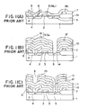
- FIGS.1(A) - 1(F) show a conventional process for fabricating a dynamic random access memory that uses the stacked fin structure for the memory cell capacitor.
- a p-type silicon substrate 1 is subjected to an oxidation process in a wet O 2 environment to form a field oxide film 1a of silicon oxide such that the field oxide film 1a covers the substrate 1 except for a device region in which the active part of the device is to be formed.
- a thin oxide film 2 of silicon oxide is formed on the surface of the substrate 1 in correspondence to the device region by a thermal oxidation process which is conducted in a dry O 2 environment.
- a polysilicon layer which is patterned subsequently to form a polysilicon word line WL.
- the word line WL extends over the oxide film 2 and acts as a gate electrode 3.
- the oxide film 2 located underneath the gate electrode 3 acts as a gate oxide film.
- an ion implantation of an n-type dopant such as As is conducted in accordance with the self-alignment process that uses the gate electrode 3 as a mask, and there are formed diffusion regions 4 and 5 in the substrate 1 at both sides of the gate electrode 3 respectively in correspondence to the drain and source of a MOS transistor.
- the MOS transistor forms a transfer gate transistor.
- a silicon oxide insulation layer 7 is deposited on the device thus formed by a CVD process such that the word line WL is buried under the insulation layer 7.
- a contact hole 8 is formed in the insulation layer 7 in correspondence to the source region 4 such that the surface of the substrate 1 and hence the source region 4 is exposed in correspondence to the contact hole 8, and a polysilicon layer is deposited on the layer 7 such that the polysilicon layer establishes a contact with the exposed surface of the source region 4.
- a polysilicon bit line is formed.
- a silicon nitride etching stopper 10 is deposited for example by a CVD process, and a silicon oxide layer 11 and a polysilicon layer 12 are deposited successively also by a CVD process. Further, another silicon oxide layer 13 is deposited on the polysilicon layer 12 similarly, and a contact hole 14 is formed through the layers 10 - 13 as well as through the underlying layers 2 and 7 to expose the upper major surface of the drain region 5 as shown in FIG.1(B).
- a polysilicon layer 15 is deposited by a CVD process to cover the upper major surface of the silicon oxide layer 13 as well as the side wall of the contact hole 14 and further the surface of the drain region 5 exposed by the contact hole 14. Further, an RIE process is applied to form a groove 6 that extends substantially vertically from the upper major surface of the polysilicon layer 15 to the upper major surface of the etching stopper 11 such that the groove 6 defines each memory cell capacitor. In other words, each memory cell capacitor is separated from adjacent memory cell capacitors by the groove 6. See the structure of FIG.1(C).
- FIG.1(C) an wet etching process using a HF etchant is applied to the structure of FIG.1(C) to dissolve the silicon oxide layers 11 and 13. Thereby, the etching acts selectively upon silicon oxide and a structure shown in FIG.1(D) is obtained. There, it will be noted that there is formed a stacked fin electrode 16 including a plurality of electrode fins formed of the polysilicon layers 12 and 15 such that the electrode structure 16 establishes a contact with the exposed upper major surface of the drain region 5.
- a silicon nitride film 17 is deposited on the exposed surface of the electrode 16 including the surface of the electrode fins 12 and 15 by a CVD process, and the structure thus formed is subjected to a thermal oxidation process for eliminating any pin holes formed in the silicon nitride film 17.
- a polysilicon layer 18 is deposited also by a CVD process as an opposing electrode such that the polysilicon layer 18 fills the gap between the electrode fins and buries the electrode 16 underneath.
- the decrease of the thickness of the electrode fin becomes essential for compensating for the decreased capacitance.
- the thickness of each electrode fin can be reduced successfully, the number of the fins and hence the capacitance of the memory cell capacitor would be increased.
- intensive investigations have been made to form the electrode fin as thin as possible.
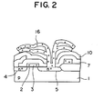
- the inventor of the present invention has discovered that there are cases wherein the electrode fins forming the stacked memory cell capacitor are deformed or bent as shown in FIG.2. When this occurs, the electrode fins are contacted with each other and the capacitance of the memory cell capacitor is decreased inevitably. It was found further that such a deformation occurs particularly in the step of FIG.1(D) for removing the oxide layers 11 and 13 by the wet etching process and in the step of providing the dielectric film 17 on the surface of the electrode fins. It is believed that the removal of the silicon oxide layer underlying the electrode fin causes the disappearance of the mechanical support of the electrode fin, and the electrode fin is subjected to a large thermal stress acting on the surface of the fin.
- Such a thermal stress is caused as a result of the difference in the thermal expansion between the polysilicon layer 12 or 15 and the silicon oxide layer 11 or 13.
- the thermal stress exceeds the yielding strength of the polysilicon layer, the fin starts to cause a ductile deformation. Further, the deposition of the dielectric film 17 and the heat treatment applied thereto contributes to the ductile deformation of the electrode fin. It should be noted that the yielding strength of materials generally decreases at elevated temperatures because of the movement of dislocations which is facilitated in such elevated temperatures.
- the deformation of the electrode fin tends to appear most conspicuously in the electrode fin at the top of the stacked fin capacitor because of the cumulative effect of the thermal stress. It should be noted that there occurs an accumulation of the stress during each deposition of the polysilicon layers and the silicon oxide layers.
- EP-A2-0 318 277 a method of fabricating a dynamic random access memory according to the preamble of claim 1 is known, wherein an additional silicon nitride film functioning as an etching stopper layer is deposited on the substrate. From EP-A3-0 295 709 a similar method providing an etching stopper layer is known.
- this object is achieved by a method as defined in claim 1.
- the problem of deformation of the electrode fin is successfully eliminated even when the thickness of the electrode fin is reduced below 100 nm, by forming the stacked fin electrode in the amorphous state and with a thickness smaller than 100 nm. It is believed that the absence of grain boundary in the amorphous silicon suppresses the ductile deformation of the electrode fin successfully. It should be noted that the ductile deformation involves a slip at the grain boundary in polycrystal materials. After the heat treatment applied at the time of depositing the dielectric film, the amorphous electrode fin crystallizes.
- the dynamic random access memory formed according to the process of the present invention is characterized by a coarse grain texture of the electrode fin as compared with other polysilicon electrodes that are formed from the beginning as the polycrystalline phase.
- These polysilicon electrodes include the word lines and the bit lines in addition to the foregoing opposing electrode.
- the present invention provides another advantageous feature that the electrode fin is formed with a uniform thickness even when the thickness of the fin is reduced below a few nanometers. It is believed that the formation of the island structure, which is pertinent to the growth of polysilicon layer on an insulator layer, is successfully eliminated by growing the fin electrode in the form of amorphous silicon. Thereby, a sufficient capacitance is secured even when the thickness of the electrode fin is reduced to a few nanometers.
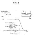
- FIG.3 shows the result of the experiments conducted for investigating the effect of the deposition temperature of the stacked fin electrode, on the occurrence of the deformation of the electrode fin, wherein FIG.3 shows the result in the form of a graph describing the percentage of deformation occurrence and the fin thickness.
- a model device shown in FIG.3 is used for the experiment, with a fin-shaped electrode EL having a lateral size 1 set to 1.7 ⁇ m.
- the device is fabricated by the steps similar to the process of FIGS.1(A) - 1(F). More specifically, the device is formed by depositing a silicon oxide layer (not shown) on a silicon substrate SB by a CVD process, forming a contact hole (not shown) on the silicon oxide layer, depositing a silicon layer on the silicon oxide layer by a CVD process and patterning the same to form the fin-shaped electrode EL in contact with the substrate at the contact hole, and removing the silicon oxide layer by a wet etching process.
- a silicon nitride film D is deposited on the surface of the electrode EL by a CVD process at 700 °C, and the structure thus formed is subjected to a thermal oxidation process at 850 °C for eliminating pin holes formed in the silicon nitride film D.
- the experiment was conducted in two series with respective CVD temperatures for the deposition of the silicon electrode EL.
- the deposition of the electrode EL was achieved at 620 °C, while in the second series, the temperature was set at 450 °C.
- monosilane SiH 4
- disilane Si 2 H 6
- the disilane gas used for the source of Si may be supplied of course with the usual He carrier gas.
- the pressure inside the reaction vessel was set at about 0.5 Torr. Thereby, a deposition rate of about 1.5 nm/min was obtained. It should be noted that, when the deposition is made at 620 °C, the silicon layer that forms the fin-shaped electrode EL is deposited as polysilicon. On the other hand, the silicon layer is deposited as an amorphous phase when the deposition is achieved at 450 °C.
- the occurrence of deformation of the fin-shaped electrode is almost eliminated when the deposition temperature is set at 450 °C, even when the thickness of the electrode fin is reduced below 100 nm. In fact, no noticeable deformation was observed even when the thickness of the fin is reduced to about 20 nm as indicated by the broken line. On the other hand, those samples that employed the deposition temperature of 620 °C showed the deformation occurring when the thickness of the fin is reduced below about 100 nm. Generally, it was found that the stacked fin electrodes provided on a smooth surface as the model device of FIG.3 experience less deformation as compared with the device of FIG.2 wherein the stacked fin electrode is provided on a non-flat surface.
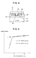
- FIGS.4 and 5 show the investigation, wherein FIG.4 shows the structure of the specimen used for the investigation and FIG.5 shows the result.
- the device used for the investigation is constructed on a p-type silicon substrate 20 and includes an n + -type diffusion region 21 that is formed at the surface of the substrate 20.
- the surface of the substrate 20 is covered by a silicon oxide film 22 having a thickness of 100 nm, and a contact hole is formed in the silicon oxide film 22 such that the diffusion region 21 is exposed.
- an electrode 23 of silicon is formed such that the electrode 23 establishes a contact with the exposed diffusion region 21, wherein the thickness of the electrode 23 is changed variously in the experiment.
- the electrode 23 is covered by a silicon nitride film 24 having a thickness of 6 nm, and a polysilicon electrode 25 is deposited to bury the electrode 23 together with the dielectric film 24 covering the electrode 23.
- the amorphous silicon deposited at low temperatures such as 450 °C covers the surface of the silicon oxide film 22 uniformly and a sufficient capacitance is secured as a result of the uniform coverage.
- the gradual decrease of the capacitance shown in FIG.5 for both the amorphous electrode and the polysilicon electrode is believed to be caused by the decrease of the thickness and hence the side wall area of the electrode.
- the result of FIG.5 clearly indicates the advantage of using amorphous silicon for the stacked fin electrode.
- the inventor of the present invention has conducted an investigation concerning the effect of the heat treatment applied to the dielectric film on the occurrence of the fin deformation.
- the silicon nitride film such as the film 17 of FIG.1(E) is formed by the CVD process that is conducted at a high temperature such as 700 °C.
- a thermal oxidation process is applied to the silicon nitride film 17 in order to eliminate short circuit of the capacitor via minute pin holes formed in the thin silicon nitride film.
- Such a thermal oxidation process also may be responsible for the deformation of the electrode fin.
- the vertical axis represents the percentage of occurrence of the deformation and the horizontal axis represents the thickness of the fin.
- a fin capacitor as shown in the same diagram is used with a fin size 1 set to 1.7 ⁇ m.
- the electrode of the fin capacitor is formed by depositing a polysilicon by a CVD process that uses a thermal decomposition of silane (SiH 4 ) at 620 °C.
- the formation of the stacked fin electrode is achieved by the process similar to the process described with reference to FIG.3 and the description will not be repeated.
- the continuous line represents the relationship for the specimen that has the stacked fin capacitor which is covered by a silicon nitride film deposited by a CVD process at 700 °C and oxidized subsequently at 850 °C
- the broken line represents the relationship for the specimen that has the stacked fin capacitor which is oxidized at 700 °C after the deposition of silicon nitride at 700 °C.
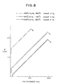
- FIG.7 shows the effect of the lateral size 1 on the occurrence of the fin deformation.
- the stacked fin capacitor is formed by polysilicon deposited by the CVD process of silane conducted at 620 °C.
- the relationship of FIG.4 indicates that the occurrence of deformation decreases when the size 1 and hence the surface area of the electrode fin is decreased. This result suggests that the deformation is caused by the thermal stress acting at the interface between the polysilicon electrode fin and the silicon nitride film that covers the electrode fin. Again, it will be seen that the deformation occurs more or less when the thickness of the electrode fin is reduced below about 100 nm even when the size 1 is reduced, as long as the fin electrode is formed of polysilicon.
- FIG.8 summarizes the foregoing findings and shows an optimum range of the fin length and the fin thickness in which the stacked fin capacitor can be fabricated without substantial deformation of the electrode fin.
- the boundary representing the allowable thickness of the electrode fin decreases with decreasing lateral size 1, reflecting the general relationship shown in FIG.3 and FIGS.5 - 7, wherein the position of the boundary changes with the depositing condition as well as with the processing condition of the electrode fin.
- the region located at the lower right side of the boundary line represents the region wherein the deformation of the electrode fin does not occur.
- the boundary represented by the continuous line indicates the case wherein the stacked fin electrode is deposited by the CVD process of monosilane at 620 °C and annealed at 850 °C in the oxidizing atmosphere after the formation of the silicon nitride film.
- the boundary represented by the broken line represents the case wherein the stacked fin electrode is deposited by the CVD process of monosilane also at 620 °C and annealed for oxidation at a lower temperature of 700 °C.
- the boundary represented by the one-dotted chain represents the case wherein the stacked fin electrode is deposited by the CVD process of disilane at 450 °C and annealed at 850 °C for oxidation.
- a p-type silicon substrate 31 corresponding to the substrate 1 of FIG.1(A) is covered by a thick field oxide film 32 of silicon oxide that corresponds to the field oxide region 1a of FIG.1(A) as well as by a thin silicon oxide film 33 that corresponds to the silicon oxide film 2 of FIG.1(A).
- the field oxide film 32 has a thickness of about 400 nm while the silicon oxide film 33 has a thickness of about 10 nm.
- a plurality of polysilicon word lines WL are provided to extend generally parallel with each other, wherein the part of the polysilicon word line WL that extends over the silicon oxide film 33 acts as a gate electrode 35 of a transfer gate transistor.
- the silicon oxide film 33 under the gate electrode 35 acts as a gate oxide film.
- the polysilicon word line WL is formed by the steps of: depositing a polysilicon layer with a thickness of about 200 nm; incorporating phosphorous ions with a concentration level of about 1 X 10 20 /cm 3 to increase the conductivity; and patterning the polysilicon layer.
- n + -type diffusion regions 36 and 37 are formed at both lateral sides of the gate electrode 35 respectively as the source and drain of the transfer gate transistor by the ion implantation process conducted by using the electrode 35 as a mask, similarly to the conventional device.
- the phosphorous ions are incorporated with a dose of about 3 X 10 13 /cm 2 .
- Tr there is formed a transfer gate transistor Tr having the diffusion region 36 as the source, the diffusion region 37 as the drain, and the polysilicon gate electrode 35 connected to the word line WL.
- a silicon oxide film 38 is provided by a CVD process as shown in FIG.1(B) with a thickness of about 100 nm as usual, and a contact hole 39 is provided through the layer 38 as well as through the layer 33 located underneath the layer 38 such that the surface of the diffusion region 36 is exposed at the contact hole 39. Further, a polysilicon layer 40 and a tungsten silicide layer 11 are deposited consecutively on the surface of the silicon oxide film 38 with respective thicknesses of 50 nm and 100 nm such that the layers 10 and 11 establish an electrical contact with the exposed upper major surface of the diffusion region 36.
- phosphorous ions are incorporated into the polysilicon layer 10 with an acceleration energy of 70 keV and a dose of 4 X 10 15 /cm 2 such that the polysilicon layer becomes conductive, and the layers 10 and 11 are patterned to form a bit line BL such that the bit line BL establishes a contact with the diffusion region 36 and acts as a source electrode 42 of the transfer gate transistor Tr. See FIG.9(B).
- a silicon nitride etching stopper 43 is formed with a thickness of 50 nm by a CVD process, and a silicon oxide layer 44 and an amorphous silicon layer 45 are deposited consecutively on the silicon nitride etching stopper 43 by a CVD process with respective thicknesses of 30 nm and 20 nm.
- the amorphous silicon layer 45 is deposited from disilane at the temperature of 400 - 550 °C, more preferably at the temperature of 450 °C as described previously with reference to FIG.3.
- the gaseous source for the deposition of amorphous silicon is not limited to disilane but monosilane can also be used though with a reduced deposition rate. Further, one may use trisilane (Si 3 H 8 ) for the same purpose. In this case, one can conduct the deposition in the temperature range of 350 °C - 500 °C. Generally, an amorphous silicon layer is obtained when the CVD process is achieved at the temperature below 500 °C.
- an ion implantation process of phosphorous is conducted with an acceleration energy of 5 keV and a dose of 4 x 10 15 /cm 2 , and another silicon oxide layer 46 is deposited on the amorphous silicon layer 45 by a CVD process with a thickness of 30 nm.
- a structure shown in FIG.9(C) is obtained.
- an annealing process for example at 600 - 700 °C for 30 - 180 minutes, after the ion implantation process.
- a photolithographic patterning is conducted to form a contact hole 47 by an RIE process such that the contact hole 47 exposes the upper major surface of the diffusion region 37 by extending through the layers 31, 38 and 43 - 46.
- an amorphous silicon layer 48 is deposited by a CVD process of disilane conducted at 450 °C such that the amorphous silicon layer 48 covers the side wall as well as the surface of the diffusion region 37 exposed at the bottom of the contact hole 47, and an ion implantation is conducted to incorporate phosphorus ions for rendering the amorphous silicon layer 48 conductive.
- the layers 45, 46 and 48 are patterned by a photolithographic process that uses an RIE process such that a groove 49 is formed to define a stacked fin electrode 50 laterally as shown in FIG.9(E).
- FIG.9(E) is subjected to a wet etching process for selectively removing the silicon oxide layers 44 and 49 with respect to the amorphous silicon layers 45 and 48.
- a wet etching process for selectively removing the silicon oxide layers 44 and 49 with respect to the amorphous silicon layers 45 and 48.
- a silicon nitride film 51 is deposited on the exposed surface of the stacked fin electrode 50 by a CVD process conducted at 800 °C with a thickness of about 7 nm, and the stacked fin electrode 50 thus covered by the silicon nitride film 51 is subjected to a thermal oxidation process conducted at about 800 °C in a wet O 2 environment.
- a silicon oxide film 52 covering the surface of the silicon nitride film 51 with a thickness of about 1 nm for eliminating the leak current caused by a pin hole formed in the silicon nitride film 51.
- the silicon nitride film 51 and the silicon oxide film 52 form together a dielectric film 53 of the memory cell capacitor.
- a deposition of polysilicon is conducted to form an opposing electrode 54 of polysilicon such that the electrode 54 buries the stacked fin electrode 50 as shown in FIG.9(H).
- the electrode 54 fills the gap formed between the electrode fins as usual in the stacked fin capacitor.
- a gas phase thermal diffusion process with POCl 3 as the source gas is applied to the electrode 54 at 800 °C for rendering the electrode 54 conductive.
- a planarizing insulation layer 55 of BPSG is provided on the electrode 54, and an interconnection conductor 56 such as the shunt word line is provided on the planarized surface of the insulation layer 55.
- FIG.10 shows the dynamic random access memory thus fabricated in the plan view.
- a device region X having an elongated rectangular shape in correspondence to the device region surrounded by the field oxide film 32 of FIG.9(A), and the contact hole 39 is formed in correspondence to the device region X.
- the bit lines BL of polysilicon are provided to extend generally parallel with each other in the lateral direction in the drawing, with an electrical connection with the diffusion region 36 at the contact hole 39.
- the other contact hole 47 is provided in the device region X to expose the diffusion region 37, and the stacked fin capacitor C, defined by a lateral boundary Y, is provided in contact with the diffusion region 37 at the contact hole 47.
- the polysilicon word lines WL extend generally parallel with each other in the vertical direction as illustrated in FIG.10.
- the contact hole 47 is provided with a lateral offset from the center of the stacked fin capacitor C such that the stacked fin capacitor C has a first lateral size 1 1 at one side of the contact hole 47 and a second, different lateral size 1 2 at the other side of the contact hole 47.
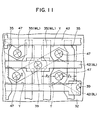
- FIG.11 shows another example of the layout of the dynamic random access memory in the plan view.
- the contact hole 39 is provided at the center of the device region X that is formed to have an elongated rectangular shape extending obliquely in the drawing.
- the bit line BL is provided in contact with the diffusion region 36 and to extend laterally in the drawing, while the word lines extend generally vertically at both sides of the contact hole 39.
- the contact holes 47 are formed at both ends of the device region X, and the stacked fin capacitor C is provided in contact with the diffusion region 37 at each contact hole 47.
- the contact hole 47 is located at the center of the capacitor and thus, the length 1 3 of the fin becomes smaller than the case of FIG.10. It should be noted that the layout shown in the plan view of FIG.10 or FIG.11 is already known and further description will be omitted.
- the stacked fin electrode 50 experiences a crystallization upon the heat treatment associated with the CVD process of the silicon nitride film 51 and the thermal oxidation process of the silicon oxide film 52.
- the electrode 50 crystallizes, it was found that there occurs a significant crystal growth in the electrode 50, resulting in a coarse grain texture characterized by the grain size which is much larger than the grain size of the polysilicon word lines WL or bit lines BL that are formed from the beginning as a polycrystalline phase.
- the grain size of the polysilicon layer is in the order of 0.2 - 0.3 ⁇ m even after the heat treatment conducted at about 800 °C.
- the dark patterns show the individual grains of silicon crystal forming the polysilicon layer.
- the attached PHOTO 2 shows the cross section of an amorphous silicon layer which was grown at 450 °C from disilane.
- PHOTO 2 showing the cross section in the same scale as in PHOTO 1, it will be noted that there exists a single boundary separating two large crystal grains.
- the word lines WL and the bit lines BL experience the heat treatment upon the formation of the dielectric film 53. Thereby, the crystal growth occurs also in these polycrystal electrodes. However, because of a competing process occurring in the grain growth between individual crystal grains in the polysilicon electrode, the growth of particular crystal is suppressed or obstructed. In the amorphous silicon electrode 50, on the other hand, the crystallization starting from a small number of nucleation sites can lead to a substantially unobstructed crystal growth, which eventually leads to a very coarse texture for the electrode 50. In fact, the grain size of the stacked fin electrode 50 is generally larger than the grain size of any of the word lines WL, bit lines BL and the opposing electrode 54 by at least about 500 nm.
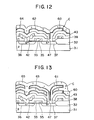
- FIG.12 shows another example of the dynamic random access memory fabricated according to the present invention corresponding to a modification of the first embodiment.
- the stacked memory cell capacitor C has only one electrode fin 60.
- the electrode fin 60 forming stacked fin electrode C is formed by depositing silicon in the amorphous state by the CVD process of disilane conducted at 450 °C.
- a dielectric film 62 is formed similarly to the dielectric film 53, and an opposing electrode 64 of polysilicon is provided to bury the stacked fin electrode 60 underneath.
- the rest of the feature of the device of FIG.12 is substantially identical with the device described previously, further description will be omitted.
- FIG.13 shows still another modification wherein the stacked fin capacitor C has two electrode fins 60 and 61 both formed as amorphous silicon layers.
- the parts other than the stacked fin capacitor C are fabricated similarly to the previous embodiments.
- an amorphous silicon layer is deposited directly on the silicon nitride etching stopper 43, and the oxide layer and amorphous silicon layer are stacked alternately on the amorphous silicon layer thus formed.
- the dynamic random access memory has a structure generally identical with the structure of the device of the previous embodiments except that the stacked fin capacitor C has three electrode fins 70 1 - 70 3 of polysilicon forming a stacked fin electrode 70.
- the stacked fin electrode 70 is thereby formed of polysilicon and is covered by a dielectric film 71 as usual. Further, an opposing electrode 72 of polysilicon covers the surface of the stacked fin electrode 70 such that the dielectric film 71 is sandwiched between the electrodes 70 and 72.
- the device of the present example is different from the previously described device in that the thickness of the electrode fin is changed depending upon the level thereof such that the fin 70 3 at the top of the stacked fin electrode 70 has an increased thickness as compared with the other electrode fins 70 1 and 70 2 locating at the lower level.
- the deformation of the electrode fin that occurs particularly conspicuous in the electrode fin 70 3 at the top of the electrode 70 due to the cumulative thermal stress is successfully eliminated.
- the deposition of the polysilicon layer forming the electrode fin and the silicon oxide layer to be etched away later induces a thermal stress at the interface between the polysilicon layer and such a thermal stress is accumulated from the lower level fin to the upper level fin.
- the result of FIG.8 clearly indicates that one can reduce or eliminate the deformation of the electrode fin when the thickness of the fin is increased.
- the present example uses a thickness of 20 nm for the fins 70 1 and 70 2 , while a thickness of 50 nm is used for the fin 70 3 .
- the stacked fin electrode 70 in the form of amorphous silicon instead of polysilicon.
- the inventor of the present invention has discovered that the deformation occurs not only at the time of the deposition of the dielectric film but also at the time when the silicon oxide layer is removed by the wet etching process as in the step of FIG.1(D). More particularly, it was discovered that the fin deformation can occur when the stacked fin electrode is dried after the wet etching has been completed. It was discovered further that such a deformation can occur in the deformation-free device when the device is immersed in purified water and dried subsequently.
- FIGS.16(A) - 16(C) show the possible mechanism of such a deformation of the electrode fin.
- FIG.16(A) showing the state wherein a water film w f fills the gap between adjacent electrode fins f 1 and f 2 , a surface tension acts at the interface between the water film w f and the electrode fin f 1 or f 2 .
- the electrode fin starts to bend as a result of the surface tension, and the deformation propagates toward the root part of the fin with the progress of the evaporation.
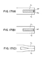
- the deformation occurs also when the etching of the silicon oxide layer is achieved by a dry etching process that uses a vapor mixture of HF and H 2 O.
- FIG.17(A) shows the state wherein the dry etching process by the mixture of a HF vapor and a H 2 O vapor has just started.
- a silicon oxide film S O to be etched, with the outer marginal part of the silicon oxide film S O slightly etched away.
- a film of a HF/H 2 O fluid which is an aqueous solution of HF.
- FIG.18(A) shows the state before the etching is started. As shown in FIG.18(A), there is formed a silicon oxide film S O between a pair of adjacent silicon electrode fins f 1 and f 2 .
- the outermost part of the silicon oxide film S O is etched away by a mixture of HF and H 2 O that are condensed from a vapor mixture of HF and H 2 O.
- reactions such as 2HF + H 2 O ⁇ H 3 O + + HF 2 - SiO 2 + 2H 3 O + + 2HF 2 - ⁇ SiF 4 + 4H 2 O SiO 2 + H 3 O + + 3HF 2 - ⁇ SiF 6 2- + 3H 2 O take place.
- the reaction (1) occurs between the HF vapor and the water vapor. This reaction may occur for example at the exposed surface of the silicon oxide film S O .
- the second reaction (2) occurs at the exposed surface of the silicon oxide film S O , and the silicon oxide film is etched by releasing SiF 4 .
- the compound SiF 4 is volatile and evaporates immediately upon formation.
- the third reaction (3) occurs when H 2 O is formed as a result of the reaction (2). Thereby, the etching reaction is enhanced by releasing SiF 6 2- which also evaporates upon formation.
- the present example avoids the problem of bending of the electrode fins by interrupting the etching process before the etching proceeds to the extent that the gap between the fins is filled by the fluid of the reaction product. More specifically, the supply of the HF vapor and H 2 O vapor is interrupted before the gap is filled by the fluid, and the supply of the etching gas is replaced with the supply of dry N 2 . As a result of the supply of dry N 2 , the fluid is removed as shown in FIG.18(C).
- the steps corresponding to FIG.9(C) for depositing the layers 44 and 46 are achieved by a plasma enhanced CVD process that employs acetylene (C 2 H 2 ) for the source gas.
- the acetylene is diluted by He or Ar, and the deposition is achieved at a pressure of 1 Torr and a temperature of 200 °C, while supplying an RF power of 32 watts at the industrial statutory frequency of 13.56 MHz.
- amorphous carbon layers are formed for the layers 44 and 46.
- the etching for forming the contact hole 47 corresponding to the process of FIG.9(D) is achieved by an RIE process conducted in the atmosphere containing oxygen. Further, the etching process corresponding to FIG.9(F) for removing the carbon layers 44 and 46 is achieved by a plasma etching process conducted in the atmosphere containing oxygen.
- the problem of surface tension caused by the fluid reactant is eliminated and the formation of the stacked fin capacitor with deformation-free electrode fins is guaranteed.
Description
- The present invention generally relates to a method for fabricating a dynamic random access memory that has a stacked fin capacitor for increased capacitance of the memory cell capacitors.
- The dynamic random access memories (DRAMs) are characterized by the simple device structure in that the device typically includes only a single memory cell capacitor for storing information and a single transfer gate transistor connected to the memory cell capacitor. Thus, the device can be fabricated easily with a large integration density and is suitable for constructing a semiconductor memory device having a large storage capacity. Currently, the devices having a storage capacity of 256 Mbits or 1 Gbits are studied intensively.
- In order to fabricate large-scale DRAMs having a large number of memory cells assembled therein, various efforts have been made so far. Such efforts of course include the development of the submicron patterning processes that are applicable to the fabrication of the DRAMs having extremely minute memory cells. Particularly, the development of optical lithography applicable to the submicron patterning is essential for the mass production of the DRAMs.
- Simultaneously, considerable efforts have been devoted for securing sufficient capacitance for the memory cell capacitors while reducing the size of the memory cells simultaneously. It should be noted that the reduction of the size of the memory cell capacitor generally invites a reduction in the capacitance of the memory cell. In the DRAMs, the capacitance of the memory cell capacitors is required to be larger than the parasitic capacitance of the bit lines.
- One obvious solution to compensate for such a decrease of the capacitance would be to increase the height of the memory cell capacitor such that a sufficient surface area is secured by the increased side wall area of the memory cell capacitor. This approach, however, causes a problem in that there appears a large difference in the level between a memory cell region wherein the memory cells are formed and a peripheral region wherein various peripheral circuits are formed. When such a large difference or step is formed on the surface of the device, the exposure of patterns particularly those extending between the memory cell region and the peripheral region across the boundary between these regions becomes extremely difficult or impossible. It should be noted that one has to use an optical system having a very large numerical aperture for conducting the exposure with submicron resolution, while the use of such a large numerical aperture inevitably reduces the focal depth of the optical system. In fact, an optical system having a focal depth in the order of 0.1 µm has been used for the submicron optical exposure. In such a submicron optical exposure, the surface irregularity caused by the tall memory cell capacitors is detrimental.
- In order to reduce the height of the memory cell capacitor and simultaneously to secure sufficient capacitance, the inventor of the present invention has proposed previously a stacked fin capacitor structure for the memory cell capacitor of the dynamic random access memories. In the stacked fin capacitor structure, a number of thin electrode plates or electrode fins are stacked with each other with a mutual separation and in connection with each other, and a thin dielectric film is deposited on the surface of the electrode fins. Further, an opposing electrode is provided to bury the stacked fin electrode by filling the space or gap formed between the electrode fins. Thereby, one can increase the surface area of the memory cell capacitor significantly without increasing the height.
- FIGS.1(A) - 1(F) show a conventional process for fabricating a dynamic random access memory that uses the stacked fin structure for the memory cell capacitor.
- Referring to FIG.1(A), a p-
type silicon substrate 1 is subjected to an oxidation process in a wet O2 environment to form a field oxide film 1a of silicon oxide such that the field oxide film 1a covers thesubstrate 1 except for a device region in which the active part of the device is to be formed. Further, athin oxide film 2 of silicon oxide is formed on the surface of thesubstrate 1 in correspondence to the device region by a thermal oxidation process which is conducted in a dry O2 environment. On thesubstrate 1 thus covered by the field oxide 1a and theoxide film 2, there is provided a polysilicon layer which is patterned subsequently to form a polysilicon word line WL. As usual, the word line WL extends over theoxide film 2 and acts as agate electrode 3. Thereby, theoxide film 2 located underneath thegate electrode 3 acts as a gate oxide film. - After the
gate electrode 3 is formed, an ion implantation of an n-type dopant such as As is conducted in accordance with the self-alignment process that uses thegate electrode 3 as a mask, and there are formeddiffusion regions substrate 1 at both sides of thegate electrode 3 respectively in correspondence to the drain and source of a MOS transistor. Thereby, the MOS transistor forms a transfer gate transistor. Next, a siliconoxide insulation layer 7 is deposited on the device thus formed by a CVD process such that the word line WL is buried under theinsulation layer 7. Further, acontact hole 8 is formed in theinsulation layer 7 in correspondence to thesource region 4 such that the surface of thesubstrate 1 and hence thesource region 4 is exposed in correspondence to thecontact hole 8, and a polysilicon layer is deposited on thelayer 7 such that the polysilicon layer establishes a contact with the exposed surface of thesource region 4. By patterning the polysilicon layer thus formed, a polysilicon bit line is formed. Thereby the structure of FIG.1(A) is obtained. - On the structure of FIG.1(A), a silicon
nitride etching stopper 10 is deposited for example by a CVD process, and a silicon oxide layer 11 and apolysilicon layer 12 are deposited successively also by a CVD process. Further, anothersilicon oxide layer 13 is deposited on thepolysilicon layer 12 similarly, and acontact hole 14 is formed through the layers 10 - 13 as well as through theunderlying layers drain region 5 as shown in FIG.1(B). - Next, a
polysilicon layer 15 is deposited by a CVD process to cover the upper major surface of thesilicon oxide layer 13 as well as the side wall of thecontact hole 14 and further the surface of thedrain region 5 exposed by thecontact hole 14. Further, an RIE process is applied to form agroove 6 that extends substantially vertically from the upper major surface of thepolysilicon layer 15 to the upper major surface of the etching stopper 11 such that thegroove 6 defines each memory cell capacitor. In other words, each memory cell capacitor is separated from adjacent memory cell capacitors by thegroove 6. See the structure of FIG.1(C). - Next, an wet etching process using a HF etchant is applied to the structure of FIG.1(C) to dissolve the
silicon oxide layers 11 and 13. Thereby, the etching acts selectively upon silicon oxide and a structure shown in FIG.1(D) is obtained. There, it will be noted that there is formed a stackedfin electrode 16 including a plurality of electrode fins formed of thepolysilicon layers electrode structure 16 establishes a contact with the exposed upper major surface of thedrain region 5. - Further, a
silicon nitride film 17 is deposited on the exposed surface of theelectrode 16 including the surface of theelectrode fins silicon nitride film 17. Further, apolysilicon layer 18 is deposited also by a CVD process as an opposing electrode such that thepolysilicon layer 18 fills the gap between the electrode fins and buries theelectrode 16 underneath. Thereby, a dynamic random access memory as shown in FIG.1(F) is obtained. In the device having the structure shown in FIG.1(F), it will be noted that the surface area of the memory cell capacitor is increased significantly without increasing the height thereof. Thus, the device has been used successfully for the dynamic random access memories having the storage capacity of up to 64 Mbits. - On the other hand, when the device having the structure of FIG.1(F) is used for the DRAMs having a larger storage capacity such as 256 Mbits or more, the decrease of the thickness of the electrode fin becomes essential for compensating for the decreased capacitance. When the thickness of each electrode fin can be reduced successfully, the number of the fins and hence the capacitance of the memory cell capacitor would be increased. Thus, intensive investigations have been made to form the electrode fin as thin as possible.
- In the effort to reduce the thickness of the electrode fin, the inventor of the present invention has discovered that there are cases wherein the electrode fins forming the stacked memory cell capacitor are deformed or bent as shown in FIG.2. When this occurs, the electrode fins are contacted with each other and the capacitance of the memory cell capacitor is decreased inevitably. It was found further that such a deformation occurs particularly in the step of FIG.1(D) for removing the
oxide layers 11 and 13 by the wet etching process and in the step of providing thedielectric film 17 on the surface of the electrode fins. It is believed that the removal of the silicon oxide layer underlying the electrode fin causes the disappearance of the mechanical support of the electrode fin, and the electrode fin is subjected to a large thermal stress acting on the surface of the fin. Such a thermal stress is caused as a result of the difference in the thermal expansion between thepolysilicon layer silicon oxide layer 11 or 13. When the thermal stress exceeds the yielding strength of the polysilicon layer, the fin starts to cause a ductile deformation. Further, the deposition of thedielectric film 17 and the heat treatment applied thereto contributes to the ductile deformation of the electrode fin. It should be noted that the yielding strength of materials generally decreases at elevated temperatures because of the movement of dislocations which is facilitated in such elevated temperatures. - Further, it was found that the deformation of the electrode fin tends to appear most conspicuously in the electrode fin at the top of the stacked fin capacitor because of the cumulative effect of the thermal stress. It should be noted that there occurs an accumulation of the stress during each deposition of the polysilicon layers and the silicon oxide layers.
- From EP-A2-0 318 277 a method of fabricating a dynamic random access memory according to the preamble of
claim 1 is known, wherein an additional silicon nitride film functioning as an etching stopper layer is deposited on the substrate. From EP-A3-0 295 709 a similar method providing an etching stopper layer is known. - From Patent Abstracts Of Japan, vol. 13, no. 531 (E-851)(3879), 28 November 1989, &JP-A-1217956, it is known to use amorphous silicon layers as lower capacitor electrodes in order to increase the dielectric strength.
- It is a general object of the present invention to provide a method of fabricating a novel and useful dynamic random access memory, wherein the foregoing problems are eliminated.
- In particular, it is the object of the present invention to provide a method of fabricating a dynamic random access memory having a stacked fin electrode for a memory cell capacitor wherein the deformation of fins forming the stacked fin electrode is successfully eliminated even when the thickness of the fin is reduced for increased storage capacity of the dynamic random acess memory.
- According to the present invention, this object is achieved by a method as defined in
claim 1. - According to the present invention, the problem of deformation of the electrode fin is successfully eliminated even when the thickness of the electrode fin is reduced below 100 nm, by forming the stacked fin electrode in the amorphous state and with a thickness smaller than 100 nm. It is believed that the absence of grain boundary in the amorphous silicon suppresses the ductile deformation of the electrode fin successfully. It should be noted that the ductile deformation involves a slip at the grain boundary in polycrystal materials. After the heat treatment applied at the time of depositing the dielectric film, the amorphous electrode fin crystallizes. Thereby, there occurs a significant grain growth in the electrode fin because of the absence of preexisting grains, and a coarse texture characterized by a small number of large grains much larger than the grains forming the opposing electrode, is obtained for the electrode fin. In the opposing electrode, which is deposited as a polycrystalline phase from the beginning, there occurs a competing process in the grain growth between individual crystals and such a competitive grain growth results in a suppressing of the selective growth of small number of crystals. Thus, the dynamic random access memory formed according to the process of the present invention is characterized by a coarse grain texture of the electrode fin as compared with other polysilicon electrodes that are formed from the beginning as the polycrystalline phase. These polysilicon electrodes include the word lines and the bit lines in addition to the foregoing opposing electrode. In addition to the foregoing advantageous feature of the resistance against ductile deformation, the present invention provides another advantageous feature that the electrode fin is formed with a uniform thickness even when the thickness of the fin is reduced below a few nanometers. It is believed that the formation of the island structure, which is pertinent to the growth of polysilicon layer on an insulator layer, is successfully eliminated by growing the fin electrode in the form of amorphous silicon. Thereby, a sufficient capacitance is secured even when the thickness of the electrode fin is reduced to a few nanometers.
- Other objects and further features of the present invention will become apparent from the following detailed description when read in conjunction with the attached drawings.
-
- FIGS.1(A) - 1(F) are diagrams showing the conventional process for fabricating a dynamic random access memory that has a stacked fin memory cell capacitor;
- FIG.2 is a diagram showing the deformation of the electrode fin occurring in the conventional fabrication process of a dynamic random access memory;
- FIG.3 is a diagram showing the frequency of occurrence of the deformation of the electrode fin as a function of the fin thickness for two different deposition conditions, one for depositing the electrode fin as a polycrystal phase and the other for depositing the electrode fin as an amorphous phase;
- FIG.4 is a diagram showing the cross section of a device used for the experiment to investigate the relationship between the capacitance of the memory cell capacitor and the condition of deposition of an electrode that forms the capacitor;
- FIG.5 is a diagram showing the relationship obtained by the experiment that uses the device of FIG.4;
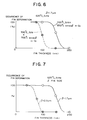
- FIG.6 is a diagram showing the frequency of occurrence of the deformation in the electrode fin as a function of the fin thickness for various heat treatment processes applied to a dielectric film that forms the memory cell capacitor;
- FIG.7 is a diagram showing the frequency of occurrence of the deformation of the electrode fin as a function of the fin thickness for various lateral sizes of the electrode fin;
- FIG.8 is a diagram showing the optimum range of the lateral size and thickness for the electrode fin that provides a successful suppressing of the fin deformation and simultaneously a sufficient capacitance as a memory cell capacitor;
- FIGS.9(A) - 9(H) are diagrams showing the fabrication process of a dynamic random access memory according to a first embodiment of the present invention;
- FIG.10 is diagram showing the dynamic random access memory fabricated according to the present invention in a plan view;
- FIG.11 is a diagram similar to FIG.10 showing another layout of the dynamic random access memory fabricated according to the process of the first embodiment;
- FIG.12 is a diagram showing another modification of the dynamic random access memory fabricated by the first embodiment process of the present invention;
- FIG.13 is a diagram showing still another modification of the dynamic random access memory fabricated by the first embodiment process of the present invention;
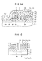
- FIG.14 is a diagram showing the structure of a dynamic random access memory;
- FIG.15 is a diagram showing a modification of the device of FIG.14;
- FIGS.16(A) - 16(C) are diagrams showing a mechanism of occurrence of the deformation of the electrode fin in the conventional fabrication process of the dynamic random access memory that employs a wet etching process for the formation of the stacked fin memory cell capacitor;
- FIGS.17(A) - 17(C) are diagrams similar to FIGS.16(A) - 16(C) showing a mechanism of occurrence of the deformation of the electrode fin in the conventional fabrication process of the dynamic random access memory that employs a dry etching process for the formation of the stacked fin memory cell capacitor; and
- FIGS.18(A) - 18(F) are diagrams showing a process for eliminating the deformation of the electrode fin.
-
-
PHOTO 1 shows the texture of a stacked fin electrode deposited in the form of polysilicon; and -
PHOTO 2 shows the texture of a stacked fin electrode deposited in the form of amorphous silicon and crystallized subsequently. - In order to understand the mechanism of deformation of the electrode fins of the stacked fin capacitor, the inventor of the present invention has conducted a series of experiments.
- FIG.3 shows the result of the experiments conducted for investigating the effect of the deposition temperature of the stacked fin electrode, on the occurrence of the deformation of the electrode fin, wherein FIG.3 shows the result in the form of a graph describing the percentage of deformation occurrence and the fin thickness.
- In the present investigation, a model device shown in FIG.3 is used for the experiment, with a fin-shaped electrode EL having a
lateral size 1 set to 1.7 µm. The device is fabricated by the steps similar to the process of FIGS.1(A) - 1(F). More specifically, the device is formed by depositing a silicon oxide layer (not shown) on a silicon substrate SB by a CVD process, forming a contact hole (not shown) on the silicon oxide layer, depositing a silicon layer on the silicon oxide layer by a CVD process and patterning the same to form the fin-shaped electrode EL in contact with the substrate at the contact hole, and removing the silicon oxide layer by a wet etching process. Further, a silicon nitride film D is deposited on the surface of the electrode EL by a CVD process at 700 °C, and the structure thus formed is subjected to a thermal oxidation process at 850 °C for eliminating pin holes formed in the silicon nitride film D. - The experiment was conducted in two series with respective CVD temperatures for the deposition of the silicon electrode EL. In the first series, the deposition of the electrode EL was achieved at 620 °C, while in the second series, the temperature was set at 450 °C. When depositing silicon at 620 °C, monosilane (SiH4) was used for the source of silicon similarly to the conventional case. When depositing the silicon electrode EL at 450 °C, on the other hand, disilane (Si2H6) was used for facilitating the deposition, with an optimum flowrate of 40 cc/min. The disilane gas used for the source of Si may be supplied of course with the usual He carrier gas. However, it was found that a more uniform thickness is obtained when the disilane gas alone is used. During the deposition, the pressure inside the reaction vessel was set at about 0.5 Torr. Thereby, a deposition rate of about 1.5 nm/min was obtained. It should be noted that, when the deposition is made at 620 °C, the silicon layer that forms the fin-shaped electrode EL is deposited as polysilicon. On the other hand, the silicon layer is deposited as an amorphous phase when the deposition is achieved at 450 °C.
- As can be seen clearly, the occurrence of deformation of the fin-shaped electrode is almost eliminated when the deposition temperature is set at 450 °C, even when the thickness of the electrode fin is reduced below 100 nm. In fact, no noticeable deformation was observed even when the thickness of the fin is reduced to about 20 nm as indicated by the broken line. On the other hand, those samples that employed the deposition temperature of 620 °C showed the deformation occurring when the thickness of the fin is reduced below about 100 nm. Generally, it was found that the stacked fin electrodes provided on a smooth surface as the model device of FIG.3 experience less deformation as compared with the device of FIG.2 wherein the stacked fin electrode is provided on a non-flat surface. Although the reason of this difference is not fully explored, it is thought probable that the absence of grain boundary in the amorphous silicon material prevents the ductile deformation of the amorphous silicon electrode EL. The result of FIG.3 encourages the use of low deposition temperature for the formation of the stacked fin capacitor.
- In order to investigate the feasibility of the low temperature deposition for forming the stacked fin capacitor, the inventor of the present invention has conducted experiments to measure the capacitance of the stacked fin capacitor while reducing the thickness of the electrode fin. FIGS.4 and 5 show the investigation, wherein FIG.4 shows the structure of the specimen used for the investigation and FIG.5 shows the result.
- Referring to FIG.4, the device used for the investigation is constructed on a p-
type silicon substrate 20 and includes an n+-type diffusion region 21 that is formed at the surface of thesubstrate 20. The surface of thesubstrate 20 is covered by asilicon oxide film 22 having a thickness of 100 nm, and a contact hole is formed in thesilicon oxide film 22 such that thediffusion region 21 is exposed. On the surface of thesilicon oxide film 22, anelectrode 23 of silicon is formed such that theelectrode 23 establishes a contact with the exposeddiffusion region 21, wherein the thickness of theelectrode 23 is changed variously in the experiment. Theelectrode 23 is covered by asilicon nitride film 24 having a thickness of 6 nm, and apolysilicon electrode 25 is deposited to bury theelectrode 23 together with thedielectric film 24 covering theelectrode 23. - In the present investigation, two series of experiments were conducted similarly to the investigation explained with reference to FIG.3, one having the
electrode 23 deposited in the form of amorphous silicon and the other having theelectrode 23 deposited in the form of polysilicon. Similarly to the investigation of FIG.3, the amorphous silicon electrode was formed by the CVD process of disilane conducted at 450 °C, while the polysilicon electrode was formed by the CVD process of monosilane at 620 °C. In each experiment, the capacitance across thediffusion region 21 and thepolysilicon electrode 25 was measured. - As shown in FIG.5 showing the result of the investigation, it was clearly demonstrated that a sufficient capacitance is secured even when the thickness of the electrode fin is reduced below about 5 nm when the electrode is formed as amorphous silicon. On the other hand, when the electrode is formed as polysilicon, the capacitance decreases rapidly when the thickness of the electrode fin is reduced below 5 nm. It is believed that the polysilicon forming the electrode fin forms an island structure on the
silicon oxide film 22 upon deposition. In such an island structure, the isolated islands of polysilicon are not connected to thediffusion region 21 electrically and do not contribute to the capacitance of the memory cell capacitor. On the other hand, it is believed that the amorphous silicon deposited at low temperatures such as 450 °C covers the surface of thesilicon oxide film 22 uniformly and a sufficient capacitance is secured as a result of the uniform coverage. The gradual decrease of the capacitance shown in FIG.5 for both the amorphous electrode and the polysilicon electrode is believed to be caused by the decrease of the thickness and hence the side wall area of the electrode. The result of FIG.5 clearly indicates the advantage of using amorphous silicon for the stacked fin electrode. - Further, the inventor of the present invention has conducted an investigation concerning the effect of the heat treatment applied to the dielectric film on the occurrence of the fin deformation. It should be noted that the silicon nitride film such as the
film 17 of FIG.1(E) is formed by the CVD process that is conducted at a high temperature such as 700 °C. Thereby, there can occur a large thermal stress at the interface between thefilm 17 and the electrode fin of the stackedfin electrode 16 because of the difference in the thermal expansion between thesilicon electrode 16 and thesilicon nitride film 17. Further, it should be noted that a thermal oxidation process is applied to thesilicon nitride film 17 in order to eliminate short circuit of the capacitor via minute pin holes formed in the thin silicon nitride film. Such a thermal oxidation process also may be responsible for the deformation of the electrode fin. - Referring to FIG.6 showing the result of the investigation, the vertical axis represents the percentage of occurrence of the deformation and the horizontal axis represents the thickness of the fin. In the experiment of FIG.6, a fin capacitor as shown in the same diagram is used with a
fin size 1 set to 1.7 µm. The electrode of the fin capacitor is formed by depositing a polysilicon by a CVD process that uses a thermal decomposition of silane (SiH4) at 620 °C. The formation of the stacked fin electrode is achieved by the process similar to the process described with reference to FIG.3 and the description will not be repeated. - In FIG.6, it should be noted that the continuous line represents the relationship for the specimen that has the stacked fin capacitor which is covered by a silicon nitride film deposited by a CVD process at 700 °C and oxidized subsequently at 850 °C, while the broken line represents the relationship for the specimen that has the stacked fin capacitor which is oxidized at 700 °C after the deposition of silicon nitride at 700 °C. In both experiments, it was shown that the deformation of the electrode fin is inevitable when the thickness of the fin is reduced below about 100 nm as long as the electrode fin is formed of polysilicon. The difference between the continuous line and the broken line is believed to reflect the effect of the thermal stress formed at the boundary between the fin and the silicon nitride film.
- FIG.7 shows the effect of the
lateral size 1 on the occurrence of the fin deformation. Again, the stacked fin capacitor is formed by polysilicon deposited by the CVD process of silane conducted at 620 °C. The relationship of FIG.4 indicates that the occurrence of deformation decreases when thesize 1 and hence the surface area of the electrode fin is decreased. This result suggests that the deformation is caused by the thermal stress acting at the interface between the polysilicon electrode fin and the silicon nitride film that covers the electrode fin. Again, it will be seen that the deformation occurs more or less when the thickness of the electrode fin is reduced below about 100 nm even when thesize 1 is reduced, as long as the fin electrode is formed of polysilicon. - FIG.8 summarizes the foregoing findings and shows an optimum range of the fin length and the fin thickness in which the stacked fin capacitor can be fabricated without substantial deformation of the electrode fin.
- As shown in FIG.8, the boundary representing the allowable thickness of the electrode fin decreases with decreasing
lateral size 1, reflecting the general relationship shown in FIG.3 and FIGS.5 - 7, wherein the position of the boundary changes with the depositing condition as well as with the processing condition of the electrode fin. In FIG.8, it should be noted that the region located at the lower right side of the boundary line represents the region wherein the deformation of the electrode fin does not occur. - In FIG.8, the boundary represented by the continuous line indicates the case wherein the stacked fin electrode is deposited by the CVD process of monosilane at 620 °C and annealed at 850 °C in the oxidizing atmosphere after the formation of the silicon nitride film. On the other hand, the boundary represented by the broken line represents the case wherein the stacked fin electrode is deposited by the CVD process of monosilane also at 620 °C and annealed for oxidation at a lower temperature of 700 °C. Further, the boundary represented by the one-dotted chain represents the case wherein the stacked fin electrode is deposited by the CVD process of disilane at 450 °C and annealed at 850 °C for oxidation. From this diagram, it will be understood that one can avoid the occurrence of the deformation of the electrode fin successfully even when the electrode fin has a
large lateral size 1, by forming the stacked fin capacitor by the CVD process conducted at low temperatures such that the stacked fin electrode is deposited in the form of amorphous silicon. - Next, a first embodiment of the present invention will be described with reference to FIGS.9(A) - 9(H).
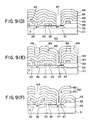
- Referring to FIG.9(A), a p-
type silicon substrate 31 corresponding to thesubstrate 1 of FIG.1(A) is covered by a thickfield oxide film 32 of silicon oxide that corresponds to the field oxide region 1a of FIG.1(A) as well as by a thinsilicon oxide film 33 that corresponds to thesilicon oxide film 2 of FIG.1(A). Typically, thefield oxide film 32 has a thickness of about 400 nm while thesilicon oxide film 33 has a thickness of about 10 nm. On the surface of thesubstrate 31 thus covered by thefield oxide film 32 and thesilicon oxide film 33, a plurality of polysilicon word lines WL are provided to extend generally parallel with each other, wherein the part of the polysilicon word line WL that extends over thesilicon oxide film 33 acts as agate electrode 35 of a transfer gate transistor. Thereby, thesilicon oxide film 33 under thegate electrode 35 acts as a gate oxide film. Typically, the polysilicon word line WL is formed by the steps of: depositing a polysilicon layer with a thickness of about 200 nm; incorporating phosphorous ions with a concentration level of about 1 X 10²⁰/cm3 to increase the conductivity; and patterning the polysilicon layer. Further, n+-type diffusion regions gate electrode 35 respectively as the source and drain of the transfer gate transistor by the ion implantation process conducted by using theelectrode 35 as a mask, similarly to the conventional device. Typically, the phosphorous ions are incorporated with a dose of about 3 X 10¹³/cm2. Thereby, there is formed a transfer gate transistor Tr having thediffusion region 36 as the source, thediffusion region 37 as the drain, and thepolysilicon gate electrode 35 connected to the word line WL. - On the surface of the structure of FIG.1(A), a
silicon oxide film 38 is provided by a CVD process as shown in FIG.1(B) with a thickness of about 100 nm as usual, and acontact hole 39 is provided through thelayer 38 as well as through thelayer 33 located underneath thelayer 38 such that the surface of thediffusion region 36 is exposed at thecontact hole 39. Further, apolysilicon layer 40 and a tungsten silicide layer 11 are deposited consecutively on the surface of thesilicon oxide film 38 with respective thicknesses of 50 nm and 100 nm such that thelayers 10 and 11 establish an electrical contact with the exposed upper major surface of thediffusion region 36. After the deposition of thelayers 10 and 11, phosphorous ions are incorporated into thepolysilicon layer 10 with an acceleration energy of 70 keV and a dose of 4X 10¹⁵/cm2 such that the polysilicon layer becomes conductive, and thelayers 10 and 11 are patterned to form a bit line BL such that the bit line BL establishes a contact with thediffusion region 36 and acts as asource electrode 42 of the transfer gate transistor Tr. See FIG.9(B). - On the structure of FIG.9(B), a silicon
nitride etching stopper 43 is formed with a thickness of 50 nm by a CVD process, and asilicon oxide layer 44 and anamorphous silicon layer 45 are deposited consecutively on the siliconnitride etching stopper 43 by a CVD process with respective thicknesses of 30 nm and 20 nm. Preferably, theamorphous silicon layer 45 is deposited from disilane at the temperature of 400 - 550 °C, more preferably at the temperature of 450 °C as described previously with reference to FIG.3. However, it should be noted that the gaseous source for the deposition of amorphous silicon is not limited to disilane but monosilane can also be used though with a reduced deposition rate. Further, one may use trisilane (Si3H8) for the same purpose. In this case, one can conduct the deposition in the temperature range of 350 °C - 500 °C. Generally, an amorphous silicon layer is obtained when the CVD process is achieved at the temperature below 500 °C. - After the deposition of the
amorphous silicon layer 45, an ion implantation process of phosphorous is conducted with an acceleration energy of 5 keV and a dose of 4 x 10¹⁵/cm2, and anothersilicon oxide layer 46 is deposited on theamorphous silicon layer 45 by a CVD process with a thickness of 30 nm. Thereby, a structure shown in FIG.9(C) is obtained. In order to reduce the thermal stress occurring at the interface between theamorphous silicon layer 45 and thesilicon oxide layer 44, one may apply an annealing process for example at 600 - 700 °C for 30 - 180 minutes, after the ion implantation process. - Next, in the step of FIG.9(D), a photolithographic patterning is conducted to form a
contact hole 47 by an RIE process such that thecontact hole 47 exposes the upper major surface of thediffusion region 37 by extending through thelayers - After the
contact hole 47 is formed as shown in FIG.9(D), anamorphous silicon layer 48 is deposited by a CVD process of disilane conducted at 450 °C such that theamorphous silicon layer 48 covers the side wall as well as the surface of thediffusion region 37 exposed at the bottom of thecontact hole 47, and an ion implantation is conducted to incorporate phosphorus ions for rendering theamorphous silicon layer 48 conductive. Next, thelayers groove 49 is formed to define astacked fin electrode 50 laterally as shown in FIG.9(E). - Next, the structure of FIG.9(E) is subjected to a wet etching process for selectively removing the silicon oxide layers 44 and 49 with respect to the amorphous silicon layers 45 and 48. Thereby, it will be seen in FIG.9(F) that the amorphous silicon layers 45 and 48 form the electrode fin of the stacked
fin electrode 50. As thelayers - In the step of FIG.9(G), a silicon nitride film 51 is deposited on the exposed surface of the stacked
fin electrode 50 by a CVD process conducted at 800 °C with a thickness of about 7 nm, and the stackedfin electrode 50 thus covered by the silicon nitride film 51 is subjected to a thermal oxidation process conducted at about 800 °C in a wet O2 environment. Thereby, there is formed a silicon oxide film 52 covering the surface of the silicon nitride film 51 with a thickness of about 1 nm for eliminating the leak current caused by a pin hole formed in the silicon nitride film 51. Thereby, the silicon nitride film 51 and the silicon oxide film 52 form together adielectric film 53 of the memory cell capacitor. - After the
dielectric film 53 is formed as shown in FIG.9(G), a deposition of polysilicon is conducted to form an opposingelectrode 54 of polysilicon such that theelectrode 54 buries the stackedfin electrode 50 as shown in FIG.9(H). There, theelectrode 54 fills the gap formed between the electrode fins as usual in the stacked fin capacitor. Further, a gas phase thermal diffusion process with POCl3 as the source gas is applied to theelectrode 54 at 800 °C for rendering theelectrode 54 conductive. Finally, aplanarizing insulation layer 55 of BPSG is provided on theelectrode 54, and aninterconnection conductor 56 such as the shunt word line is provided on the planarized surface of theinsulation layer 55. Thereby, the fabrication of the dynamic random access memory is completed. - FIG.10 shows the dynamic random access memory thus fabricated in the plan view.
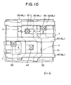
- Referring to FIG.10, there is formed a device region X having an elongated rectangular shape in correspondence to the device region surrounded by the
field oxide film 32 of FIG.9(A), and thecontact hole 39 is formed in correspondence to the device region X. Further, the bit lines BL of polysilicon are provided to extend generally parallel with each other in the lateral direction in the drawing, with an electrical connection with thediffusion region 36 at thecontact hole 39. Further, theother contact hole 47 is provided in the device region X to expose thediffusion region 37, and the stacked fin capacitor C, defined by a lateral boundary Y, is provided in contact with thediffusion region 37 at thecontact hole 47. Between the contact holes 39 and 47, the polysilicon word lines WL extend generally parallel with each other in the vertical direction as illustrated in FIG.10. In the illustrated example, thecontact hole 47 is provided with a lateral offset from the center of the stacked fin capacitor C such that the stacked fin capacitor C has afirst lateral size 11 at one side of thecontact hole 47 and a second,different lateral size 12 at the other side of thecontact hole 47. - FIG.11 shows another example of the layout of the dynamic random access memory in the plan view. In the present example, the
contact hole 39 is provided at the center of the device region X that is formed to have an elongated rectangular shape extending obliquely in the drawing. In correspondence to thecontact hole 39, the bit line BL is provided in contact with thediffusion region 36 and to extend laterally in the drawing, while the word lines extend generally vertically at both sides of thecontact hole 39. Further, the contact holes 47 are formed at both ends of the device region X, and the stacked fin capacitor C is provided in contact with thediffusion region 37 at eachcontact hole 47. In the present structure, thecontact hole 47 is located at the center of the capacitor and thus, thelength 13 of the fin becomes smaller than the case of FIG.10. It should be noted that the layout shown in the plan view of FIG.10 or FIG.11 is already known and further description will be omitted. - In the dynamic random access memory fabricated according to the process described heretofore, it should be noted that the stacked
fin electrode 50 experiences a crystallization upon the heat treatment associated with the CVD process of the silicon nitride film 51 and the thermal oxidation process of the silicon oxide film 52. When theelectrode 50 crystallizes, it was found that there occurs a significant crystal growth in theelectrode 50, resulting in a coarse grain texture characterized by the grain size which is much larger than the grain size of the polysilicon word lines WL or bit lines BL that are formed from the beginning as a polycrystalline phase. - As shown in the attached
PHOTO 1 showing the cross section of a polysilicon layer grown from monosilane at 620 °C, the grain size of the polysilicon layer is in the order of 0.2 - 0.3 µm even after the heat treatment conducted at about 800 °C. InPHOTO 1, the dark patterns show the individual grains of silicon crystal forming the polysilicon layer. On the other hand, the attachedPHOTO 2 shows the cross section of an amorphous silicon layer which was grown at 450 °C from disilane. InPHOTO 2 showing the cross section in the same scale as inPHOTO 1, it will be noted that there exists a single boundary separating two large crystal grains. These photographs clearly demonstrate the coarse texture of the stackedfin electrode 50 as compared with polysilicon electrodes such as the word line WL, bit line BL or the opposingelectrode 54. - It should be noted that the word lines WL and the bit lines BL experience the heat treatment upon the formation of the
dielectric film 53. Thereby, the crystal growth occurs also in these polycrystal electrodes. However, because of a competing process occurring in the grain growth between individual crystal grains in the polysilicon electrode, the growth of particular crystal is suppressed or obstructed. In theamorphous silicon electrode 50, on the other hand, the crystallization starting from a small number of nucleation sites can lead to a substantially unobstructed crystal growth, which eventually leads to a very coarse texture for theelectrode 50. In fact, the grain size of the stackedfin electrode 50 is generally larger than the grain size of any of the word lines WL, bit lines BL and the opposingelectrode 54 by at least about 500 nm. - FIG.12 shows another example of the dynamic random access memory fabricated according to the present invention corresponding to a modification of the first embodiment. In the present embodiment, the stacked memory cell capacitor C has only one
electrode fin 60. Similarly to the first embodiment, theelectrode fin 60 forming stacked fin electrode C is formed by depositing silicon in the amorphous state by the CVD process of disilane conducted at 450 °C. On the surface of theelectrode fin 60, adielectric film 62 is formed similarly to thedielectric film 53, and an opposingelectrode 64 of polysilicon is provided to bury the stackedfin electrode 60 underneath. As the rest of the feature of the device of FIG.12 is substantially identical with the device described previously, further description will be omitted. - FIG.13 shows still another modification wherein the stacked fin capacitor C has two
electrode fins nitride etching stopper 43, and the oxide layer and amorphous silicon layer are stacked alternately on the amorphous silicon layer thus formed. As the rest of the feature of the present invention is obvious from the preceding description, further description will be omitted. - Next, another example for eliminating the deformation of the electrode fin will be described with reference to FIG.14.
- Referring to FIG.14, it will be noted that the dynamic random access memory according to the present embodiment has a structure generally identical with the structure of the device of the previous embodiments except that the stacked fin capacitor C has three electrode fins 701 - 703 of polysilicon forming a
stacked fin electrode 70. The stackedfin electrode 70 is thereby formed of polysilicon and is covered by adielectric film 71 as usual. Further, an opposing electrode 72 of polysilicon covers the surface of the stackedfin electrode 70 such that thedielectric film 71 is sandwiched between theelectrodes 70 and 72. - On the other hand, the device of the present example is different from the previously described device in that the thickness of the electrode fin is changed depending upon the level thereof such that the
fin 703 at the top of the stackedfin electrode 70 has an increased thickness as compared with theother electrode fins electrode fin 703 at the top of theelectrode 70 due to the cumulative thermal stress, is successfully eliminated. As already noted, the deposition of the polysilicon layer forming the electrode fin and the silicon oxide layer to be etched away later induces a thermal stress at the interface between the polysilicon layer and such a thermal stress is accumulated from the lower level fin to the upper level fin. On the other hand, the result of FIG.8 clearly indicates that one can reduce or eliminate the deformation of the electrode fin when the thickness of the fin is increased. Thus, the present example uses a thickness of 20 nm for thefins fin 703. Of course, one may form the stackedfin electrode 70 in the form of amorphous silicon instead of polysilicon. Further, one may increase the thickness of the fins gradually from the bottom to the top as indicated in FIG.15. - Next, a further example will be described first with reference to FIGS.16(A) - 16(C) and FIGS.17(A) - 17(C) and later with reference to FIG.18(A) - 18(F).
- In the investigation conducted in search of the possible cause of the electrode fin deformation, the inventor of the present invention has discovered that the deformation occurs not only at the time of the deposition of the dielectric film but also at the time when the silicon oxide layer is removed by the wet etching process as in the step of FIG.1(D). More particularly, it was discovered that the fin deformation can occur when the stacked fin electrode is dried after the wet etching has been completed. It was discovered further that such a deformation can occur in the deformation-free device when the device is immersed in purified water and dried subsequently.
- FIGS.16(A) - 16(C) show the possible mechanism of such a deformation of the electrode fin. As shown in FIG.16(A) showing the state wherein a water film wf fills the gap between adjacent electrode fins f1 and f2, a surface tension acts at the interface between the water film wf and the electrode fin f1 or f2. With the evaporation occurring as shown in FIG.16(B), the electrode fin starts to bend as a result of the surface tension, and the deformation propagates toward the root part of the fin with the progress of the evaporation.
- Further, it was discovered that the deformation occurs also when the etching of the silicon oxide layer is achieved by a dry etching process that uses a vapor mixture of HF and H2O.
- FIG.17(A) shows the state wherein the dry etching process by the mixture of a HF vapor and a H2O vapor has just started. There, it can be seen that the gap between the adjacent fins f1 and f2 is still filled by a silicon oxide film SO to be etched, with the outer marginal part of the silicon oxide film SO slightly etched away. In correspondence to the part that has been etched, there is formed a film of a HF/H2O fluid which is an aqueous solution of HF. With the progress of the etching, the silicon oxide film SO is removed completely and the gap is now filled completely by the film of the HF/H2O fluid. When the HF film is removed by drying, the surface tension acting at the surface of the fin causes the bending as shown in FIG.17(C).
- In the effort to eliminate these problems that occur particularly at the time of drying, the inventor of the present invention has discovered that a stepwise and alternate progress of etching and drying can solve the problem of bending. Hereinafter, this finding will be explained with reference to FIGS.18(A) - 18(F).
- FIG.18(A) shows the state before the etching is started. As shown in FIG.18(A), there is formed a silicon oxide film SO between a pair of adjacent silicon electrode fins f1 and f2.
- In the step of FIG.18(B), the outermost part of the silicon oxide film SO is etched away by a mixture of HF and H2O that are condensed from a vapor mixture of HF and H2O. In this state, it is believed that reactions such as


- First, the reaction (1) occurs between the HF vapor and the water vapor. This reaction may occur for example at the exposed surface of the silicon oxide film SO. Next, the second reaction (2) occurs at the exposed surface of the silicon oxide film SO, and the silicon oxide film is etched by releasing SiF4. The compound SiF4 is volatile and evaporates immediately upon formation. Further, the third reaction (3) occurs when H2O is formed as a result of the reaction (2). Thereby, the etching reaction is enhanced by releasing SiF6 2- which also evaporates upon formation.
- When the reaction is continued in the state of FIG.18(B), the etching proceeds deeply into the space or gap formed between the electrode fins and the gap is filled by the fluid HF/H2O. It should be noted that this situation is exactly the same as the situation in FIG.17(B). Upon evaporation of the fluid between the gap, the bending of the electrode fin cannot be avoided.
- The present example avoids the problem of bending of the electrode fins by interrupting the etching process before the etching proceeds to the extent that the gap between the fins is filled by the fluid of the reaction product. More specifically, the supply of the HF vapor and H2O vapor is interrupted before the gap is filled by the fluid, and the supply of the etching gas is replaced with the supply of dry N2. As a result of the supply of dry N2, the fluid is removed as shown in FIG.18(C).
- In the state of FIG.18(C), a substantial part of the silicon oxide film SO remains unetched, and the etching process is restarted by resuming the supply of the HF vapor and H2O vapor. Again, the etching is interrupted before the gap is filled completely by the fluid by interrupting the supply of the HF/H2O vapor. See FIG.18(D).
- After the supply of the vapor is interrupted, the reactant fluid filling the gap partially is removed by supplying a dry N2 gas. Thereby, a state as shown in FIG.18(E) is obtained. Thus, by repeating the supply of the vapor and the supply of dry N2 alternately, one can obtain the structure shown in FIG.18(F) wherein the silicon oxide film SO is eliminated completely while maintaining the electrode fins f1 and f2 substantially free from deformation.
- It should be noted that the technique described with reference to the further example of Figs. 16A-16C is particularly useful for extending the deformation-free region as defined in FIG.8 particularly with respect to the device that has the stacked fin electrode formed as amorphous silicon.
- Further, one may avoid the problem of deformation of the electrode fin associated with the etching by employing amorphous carbon for the material filling the gap between the electrode fins. In this approach, the steps corresponding to FIG.9(C) for depositing the
layers layers contact hole 47 corresponding to the process of FIG.9(D) is achieved by an RIE process conducted in the atmosphere containing oxygen. Further, the etching process corresponding to FIG.9(F) for removing the carbon layers 44 and 46 is achieved by a plasma etching process conducted in the atmosphere containing oxygen. In the present embodiment, the problem of surface tension caused by the fluid reactant is eliminated and the formation of the stacked fin capacitor with deformation-free electrode fins is guaranteed.
Claims (8)
- A method for fabricating a dynamic random access memory having a fin capacitor electrode, said method comprising the steps of:forming a diffusion region (37) of a first conductivity type in a semiconductor substrate (31) of a second, opposite conductivity type;depositing an etching stopper layer (43), which is immune to an etching process, over said substrate (31);providing a first spacer layer (46) over said etching stopper layer (43);forming a contact hole (47) in said spacer layer (46) such that said diffusion region (37) is exposed at said contact hole;depositing a conductor layer (48) on an upper major surface of said first spacer layer (46) such that said conductor layer invades into said contact hole;patterning said conductor layer (48) to form a fin capacitor electrode (50) such that said capacitor electrode is in contact with said diffusion region (37) at said contact hole (47);removing said first spacer layer (46) by a wet etching process while leaving said etching stopper layer (43) and said fin capacitor electrode substantially intact;depositing a dielectric film (53) on said fin capacitor electrode such that said dielectric film covers upper and lower major surfaces of said fin capacitor electrode and further an exposed sidewall of said fin capacitor electrode; anddepositing a conductor material to form an opposing electrode (54) such that said opposing electrode buries said capacitor electrode underneath while establishing an intimate contact with said dielectric film (53) that covers said capacitor electrode,characterized in that
said conductor layer (48) is deposited in the armorphous state with a thickness smaller than 100 nm. - A method according to claim 1,
characterized in that
said step of depositing said amorphous conductor layer (48) is achieved by a CVD process at a temperature below about 500°C. - A method according to claim 2,
characterized in that
said CVD process is conducted by a thermal decomposition of disilane at a temperature of about 450°C. - A method according to claim 2,
characterized in that
said CVD process is conducted by a thermal decomposition of trisilane at a temperature between 350°C and 500°C. - A method according to anyone of claims 1-4,
characterized by further comprising the steps ofafter said step of depositing said etching stopper layer (43) but before said step of providing said first spacer layer (46), depositing consecutively a second spacer layer (44) and a second conductor layer (45) on said etching stopper layer (43) such that said second conductor layer is deposited in the armorphous state and having a thickness smaller than 100 nm; andafter said step of patterning said conductor layer (48), removing said second spacer layer (44) by a wet etching process while leaving said etching stopper layer (43) and said fin capacitor electrode substantially intact said fin capacitor electrode being constituted by said first and second conductor layers (48,45). - A method according to claim 5,
characterized in that
said step of depositing said second spacer layer (44) and said second conductor layer (45) is consecutively repeated a plurality of times. - A method according to claim 5 or 6,
characterized in that
said step of depositing said dielectric film (53) is conducted such that said dielectric film (53) covers further an exposed surface of said second conductor layer (45). - A method according to anyone of claims 5-7,
characterized in that
said first and second conductor layers (45, 48) comprise silicon, and said first and second spacer layers (44, 46) comprise silicon oxide.
Priority Applications (1)
| Application Number | Priority Date | Filing Date | Title |
|---|---|---|---|
| EP97103295A EP0782195B1 (en) | 1991-07-25 | 1992-07-17 | Method for dynamic random access memory having a stacked fin capacitor with reduced fin thickness |
Applications Claiming Priority (6)
| Application Number | Priority Date | Filing Date | Title |
|---|---|---|---|
| JP186155/91 | 1991-07-25 | ||
| JP3186155A JP2827181B2 (en) | 1991-07-25 | 1991-07-25 | Semiconductor device and manufacturing method thereof |
| JP239045/91 | 1991-09-19 | ||
| JP3239045A JP3044861B2 (en) | 1991-09-19 | 1991-09-19 | Semiconductor storage device |
| JP31754/92 | 1992-02-19 | ||
| JP4031754A JPH05235292A (en) | 1992-02-19 | 1992-02-19 | Manufacture of fin structure |
Related Child Applications (2)
| Application Number | Title | Priority Date | Filing Date |
|---|---|---|---|
| EP97103295A Division EP0782195B1 (en) | 1991-07-25 | 1992-07-17 | Method for dynamic random access memory having a stacked fin capacitor with reduced fin thickness |
| EP97103295.8 Division-Into | 1997-02-27 |
Publications (3)
| Publication Number | Publication Date |
|---|---|
| EP0528183A2 EP0528183A2 (en) | 1993-02-24 |
| EP0528183A3 EP0528183A3 (en) | 1993-05-12 |
| EP0528183B1 true EP0528183B1 (en) | 1997-10-08 |
Family
ID=27287451
Family Applications (2)
| Application Number | Title | Priority Date | Filing Date |
|---|---|---|---|
| EP92112279A Expired - Lifetime EP0528183B1 (en) | 1991-07-25 | 1992-07-17 | Method for fabricating a dynamic random access memory having a stacked fin capacitor with reduced fin thickness |
| EP97103295A Expired - Lifetime EP0782195B1 (en) | 1991-07-25 | 1992-07-17 | Method for dynamic random access memory having a stacked fin capacitor with reduced fin thickness |
Family Applications After (1)
| Application Number | Title | Priority Date | Filing Date |
|---|---|---|---|
| EP97103295A Expired - Lifetime EP0782195B1 (en) | 1991-07-25 | 1992-07-17 | Method for dynamic random access memory having a stacked fin capacitor with reduced fin thickness |
Country Status (4)
| Country | Link |
|---|---|
| US (1) | US5661340A (en) |
| EP (2) | EP0528183B1 (en) |
| KR (1) | KR960005243B1 (en) |
| DE (1) | DE69230156T2 (en) |
Families Citing this family (14)
| Publication number | Priority date | Publication date | Assignee | Title |
|---|---|---|---|---|
| US5525534A (en) * | 1992-03-13 | 1996-06-11 | Fujitsu Limited | Method of producing a semiconductor device using a reticle having a polygonal shaped hole |
| JPH09129848A (en) * | 1995-11-06 | 1997-05-16 | Mitsubishi Electric Corp | Manufacture of semiconductor device having capacitor |
| US5879988A (en) * | 1996-06-12 | 1999-03-09 | Mosel Vitelic Incorporated | Capacitor of a DRAM cell and method of making same |
| KR100250174B1 (en) * | 1996-06-14 | 2000-04-01 | 흥 치우 후 | Method of making capacitor of a dram cell |
| JPH10144886A (en) * | 1996-09-11 | 1998-05-29 | Toshiba Corp | Semiconductor device and fabrication thereof |
| CN1063288C (en) * | 1997-05-23 | 2001-03-14 | 联华电子股份有限公司 | Structure and mfg. method for NAND logical non crystalline silicon read-only memory device |
| US6022782A (en) * | 1997-05-30 | 2000-02-08 | Stmicroelectronics, Inc. | Method for forming integrated circuit transistors using sacrificial spacer |
| US5885867A (en) * | 1997-12-03 | 1999-03-23 | Samsung Electronics Co., Ltd. | Methods of forming hemispherical grained silicon layers including anti-nucleation gases |
| KR100339244B1 (en) | 1999-06-30 | 2002-05-31 | 박종섭 | A method of fabricating high load register type SRAM |
| DE10016971A1 (en) * | 2000-04-06 | 2001-10-11 | Angew Solarenergie Ase Gmbh | Process for coating and/or treating a surface of a substrate used in the production of semiconductor elements such as thin layer solar cells comprises bombarding the surface |
| US6559017B1 (en) * | 2002-06-13 | 2003-05-06 | Advanced Micro Devices, Inc. | Method of using amorphous carbon as spacer material in a disposable spacer process |
| JP4085891B2 (en) * | 2003-05-30 | 2008-05-14 | ソニー株式会社 | Semiconductor device and manufacturing method thereof |
| US7102204B2 (en) * | 2004-06-29 | 2006-09-05 | International Business Machines Corporation | Integrated SOI fingered decoupling capacitor |
| CN105845630B (en) * | 2015-01-13 | 2019-03-12 | 旺宏电子股份有限公司 | A kind of memory device and its manufacturing method |
Citations (4)
| Publication number | Priority date | Publication date | Assignee | Title |
|---|---|---|---|---|
| EP0295709A2 (en) * | 1987-06-17 | 1988-12-21 | Fujitsu Limited | Dynamic random access memory device and method of producing the same |
| US4994404A (en) * | 1989-08-28 | 1991-02-19 | Motorola, Inc. | Method for forming a lightly-doped drain (LDD) structure in a semiconductor device |
| EP0415530A1 (en) * | 1989-07-05 | 1991-03-06 | Fujitsu Limited | Semiconductor memory device having stacked capacitor and method of producing the same |
| EP0449000A2 (en) * | 1990-03-08 | 1991-10-02 | Fujitsu Limited | Layer structure having contact hole for fin-shaped capacitors in DRAMS and method of producing the same |
Family Cites Families (5)
| Publication number | Priority date | Publication date | Assignee | Title |
|---|---|---|---|---|
| JPS634670A (en) * | 1986-06-25 | 1988-01-09 | Hitachi Ltd | Manufacture of semiconductor integrated circuit device |
| JPS6481227A (en) * | 1987-09-24 | 1989-03-27 | Hitachi Ltd | Etching method |
| KR910009805B1 (en) * | 1987-11-25 | 1991-11-30 | 후지쓰 가부시끼가이샤 | Dynamic random access memory device and method of fabrication therefor |
| JP2835723B2 (en) * | 1988-02-26 | 1998-12-14 | 富士通株式会社 | Capacitor and method of manufacturing capacitor |
| US5223729A (en) * | 1990-09-26 | 1993-06-29 | Matsushita Electric Industrial Co., Ltd. | Semiconductor device and a method of producing the same |
-
1992
- 1992-07-17 DE DE69230156T patent/DE69230156T2/en not_active Expired - Fee Related
- 1992-07-17 EP EP92112279A patent/EP0528183B1/en not_active Expired - Lifetime
- 1992-07-17 EP EP97103295A patent/EP0782195B1/en not_active Expired - Lifetime
- 1992-07-24 KR KR1019920013316A patent/KR960005243B1/en not_active IP Right Cessation
-
1993
- 1993-10-26 US US08/141,691 patent/US5661340A/en not_active Expired - Fee Related
Patent Citations (4)
| Publication number | Priority date | Publication date | Assignee | Title |
|---|---|---|---|---|
| EP0295709A2 (en) * | 1987-06-17 | 1988-12-21 | Fujitsu Limited | Dynamic random access memory device and method of producing the same |
| EP0415530A1 (en) * | 1989-07-05 | 1991-03-06 | Fujitsu Limited | Semiconductor memory device having stacked capacitor and method of producing the same |
| US4994404A (en) * | 1989-08-28 | 1991-02-19 | Motorola, Inc. | Method for forming a lightly-doped drain (LDD) structure in a semiconductor device |
| EP0449000A2 (en) * | 1990-03-08 | 1991-10-02 | Fujitsu Limited | Layer structure having contact hole for fin-shaped capacitors in DRAMS and method of producing the same |
Also Published As
| Publication number | Publication date |
|---|---|
| US5661340A (en) | 1997-08-26 |
| EP0528183A2 (en) | 1993-02-24 |
| EP0782195B1 (en) | 1999-10-13 |
| DE69230156D1 (en) | 1999-11-18 |
| EP0782195A3 (en) | 1997-11-05 |
| EP0528183A3 (en) | 1993-05-12 |
| KR960005243B1 (en) | 1996-04-23 |
| DE69230156T2 (en) | 2000-05-25 |
| EP0782195A2 (en) | 1997-07-02 |
Similar Documents
| Publication | Publication Date | Title |
|---|---|---|
| US5464791A (en) | Method of fabricating a micro-trench storage capacitor | |
| US5091761A (en) | Semiconductor device having an arrangement of IGFETs and capacitors stacked thereover | |
| EP0750347B1 (en) | Dynamic random access memory device and method of producing the same | |
| US5913119A (en) | Method of selective growth of a hemispherical grain silicon layer on the outer sides of a crown shaped DRAM capacitor structure | |
| EP0528183B1 (en) | Method for fabricating a dynamic random access memory having a stacked fin capacitor with reduced fin thickness | |
| US7432152B2 (en) | Methods of forming HSG layers and devices | |
| KR960012254B1 (en) | Semiconductor device and manufacturing method thereof | |
| US6709919B2 (en) | Method for making auto-self-aligned top electrodes for DRAM capacitors with improved capacitor-to-bit-line-contact overlay margin | |
| US6198121B1 (en) | Method fabricating a DRAM cell with an area equal to four times the used minimum feature | |
| US6037219A (en) | One step in situ doped amorphous silicon layers used for selective hemispherical grain silicon formation for crown shaped capacitor applications | |
| JP2007110088A (en) | Semiconductor integrated circuit device and method for manufacturing the same | |
| US6384437B1 (en) | Low-leakage DRAM structures using selective silicon epitaxial growth (SEG) on an insulating layer | |
| JP2000058652A (en) | Manufacture of contact hole for semiconductor device | |
| US5292679A (en) | Process for producing a semiconductor memory device having memory cells including transistors and capacitors | |
| US6127221A (en) | In situ, one step, formation of selective hemispherical grain silicon layer, and a nitride-oxide dielectric capacitor layer, for a DRAM application | |
| JP3230663B2 (en) | Manufacturing method of cylindrical stack electrode | |
| US5792688A (en) | Method to increase the surface area of a storage node electrode, of an STC structure, for DRAM devices, via formation of polysilicon columns | |
| JP4950373B2 (en) | Semiconductor manufacturing method | |
| US5650647A (en) | Dynamic random access memory device and method of producing same | |
| JPH07109877B2 (en) | Semiconductor memory device and manufacturing method thereof | |
| US6040230A (en) | Method of forming a nano-rugged silicon-containing layer | |
| JP3407022B2 (en) | Semiconductor device, method of manufacturing the same, and semiconductor storage device | |
| US6291293B1 (en) | Method for fabricating an open can-type stacked capacitor on an uneven surface | |
| JP2530175B2 (en) | Method for manufacturing semiconductor memory device | |
| JP3085831B2 (en) | Method for manufacturing semiconductor device |
Legal Events
| Date | Code | Title | Description |
|---|---|---|---|
| PUAI | Public reference made under article 153(3) epc to a published international application that has entered the european phase |
Free format text: ORIGINAL CODE: 0009012 |
|
| AK | Designated contracting states |
Kind code of ref document: A2 Designated state(s): DE FR GB IT |
|
| PUAL | Search report despatched |
Free format text: ORIGINAL CODE: 0009013 |
|
| AK | Designated contracting states |
Kind code of ref document: A3 Designated state(s): DE FR GB IT |
|
| 17P | Request for examination filed |
Effective date: 19930812 |
|
| 17Q | First examination report despatched |
Effective date: 19950428 |
|
| GRAG | Despatch of communication of intention to grant |
Free format text: ORIGINAL CODE: EPIDOS AGRA |
|
| GRAH | Despatch of communication of intention to grant a patent |
Free format text: ORIGINAL CODE: EPIDOS IGRA |
|
| RBV | Designated contracting states (corrected) |
Designated state(s): GB IT |
|
| REG | Reference to a national code |
Ref country code: DE Ref legal event code: 8566 |
|
| GRAH | Despatch of communication of intention to grant a patent |
Free format text: ORIGINAL CODE: EPIDOS IGRA |
|
| GRAA | (expected) grant |
Free format text: ORIGINAL CODE: 0009210 |
|
| AK | Designated contracting states |
Kind code of ref document: B1 Designated state(s): GB IT |
|
| XX | Miscellaneous (additional remarks) |
Free format text: TEILANMELDUNG 97103295.8 EINGEREICHT AM 27/02/97. |
|
| ITF | It: translation for a ep patent filed |
Owner name: STUDIO JAUMANN P. & C. S.N.C. |
|
| PLBE | No opposition filed within time limit |
Free format text: ORIGINAL CODE: 0009261 |
|
| STAA | Information on the status of an ep patent application or granted ep patent |
Free format text: STATUS: NO OPPOSITION FILED WITHIN TIME LIMIT |
|
| 26N | No opposition filed | ||
| REG | Reference to a national code |
Ref country code: GB Ref legal event code: IF02 |
|
| PGFP | Annual fee paid to national office [announced via postgrant information from national office to epo] |
Ref country code: IT Payment date: 20080731 Year of fee payment: 17 |
|
| PGFP | Annual fee paid to national office [announced via postgrant information from national office to epo] |
Ref country code: GB Payment date: 20080723 Year of fee payment: 17 |
|
| GBPC | Gb: european patent ceased through non-payment of renewal fee |
Effective date: 20090717 |
|
| PG25 | Lapsed in a contracting state [announced via postgrant information from national office to epo] |
Ref country code: GB Free format text: LAPSE BECAUSE OF NON-PAYMENT OF DUE FEES Effective date: 20090717 |
|
| PG25 | Lapsed in a contracting state [announced via postgrant information from national office to epo] |
Ref country code: IT Free format text: LAPSE BECAUSE OF NON-PAYMENT OF DUE FEES Effective date: 20090717 |