EP0526972B1 - Improvements in security enclosures - Google Patents
Improvements in security enclosures Download PDFInfo
- Publication number
- EP0526972B1 EP0526972B1 EP92305197A EP92305197A EP0526972B1 EP 0526972 B1 EP0526972 B1 EP 0526972B1 EP 92305197 A EP92305197 A EP 92305197A EP 92305197 A EP92305197 A EP 92305197A EP 0526972 B1 EP0526972 B1 EP 0526972B1
- Authority
- EP
- European Patent Office
- Prior art keywords
- layer
- lines
- enclosure
- insulating material
- laminate
- Prior art date
- Legal status (The legal status is an assumption and is not a legal conclusion. Google has not performed a legal analysis and makes no representation as to the accuracy of the status listed.)
- Expired - Lifetime
Links
Images


Classifications
-
- G—PHYSICS
- G08—SIGNALLING
- G08B—SIGNALLING SYSTEMS, e.g. PERSONAL CALLING SYSTEMS; ORDER TELEGRAPHS; ALARM SYSTEMS
- G08B13/00—Burglar, theft or intruder alarms
- G08B13/02—Mechanical actuation
- G08B13/12—Mechanical actuation by the breaking or disturbance of stretched cords or wires
- G08B13/126—Mechanical actuation by the breaking or disturbance of stretched cords or wires for a housing, e.g. a box, a safe, or a room
- G08B13/128—Mechanical actuation by the breaking or disturbance of stretched cords or wires for a housing, e.g. a box, a safe, or a room the housing being an electronic circuit unit, e.g. memory or CPU chip
-
- E—FIXED CONSTRUCTIONS
- E05—LOCKS; KEYS; WINDOW OR DOOR FITTINGS; SAFES
- E05G—SAFES OR STRONG-ROOMS FOR VALUABLES; BANK PROTECTION DEVICES; SAFETY TRANSACTION PARTITIONS
- E05G1/00—Safes or strong-rooms for valuables
- E05G1/10—Safes or strong-rooms for valuables with alarm, signal or indicator
-
- Y—GENERAL TAGGING OF NEW TECHNOLOGICAL DEVELOPMENTS; GENERAL TAGGING OF CROSS-SECTIONAL TECHNOLOGIES SPANNING OVER SEVERAL SECTIONS OF THE IPC; TECHNICAL SUBJECTS COVERED BY FORMER USPC CROSS-REFERENCE ART COLLECTIONS [XRACs] AND DIGESTS
- Y10—TECHNICAL SUBJECTS COVERED BY FORMER USPC
- Y10S—TECHNICAL SUBJECTS COVERED BY FORMER USPC CROSS-REFERENCE ART COLLECTIONS [XRACs] AND DIGESTS
- Y10S206/00—Special receptacle or package
- Y10S206/807—Tamper proof
-
- Y—GENERAL TAGGING OF NEW TECHNOLOGICAL DEVELOPMENTS; GENERAL TAGGING OF CROSS-SECTIONAL TECHNOLOGIES SPANNING OVER SEVERAL SECTIONS OF THE IPC; TECHNICAL SUBJECTS COVERED BY FORMER USPC CROSS-REFERENCE ART COLLECTIONS [XRACs] AND DIGESTS
- Y10—TECHNICAL SUBJECTS COVERED BY FORMER USPC
- Y10S—TECHNICAL SUBJECTS COVERED BY FORMER USPC CROSS-REFERENCE ART COLLECTIONS [XRACs] AND DIGESTS
- Y10S428/00—Stock material or miscellaneous articles
- Y10S428/914—Transfer or decalcomania
- Y10S428/915—Fraud or tamper detecting
-
- Y—GENERAL TAGGING OF NEW TECHNOLOGICAL DEVELOPMENTS; GENERAL TAGGING OF CROSS-SECTIONAL TECHNOLOGIES SPANNING OVER SEVERAL SECTIONS OF THE IPC; TECHNICAL SUBJECTS COVERED BY FORMER USPC CROSS-REFERENCE ART COLLECTIONS [XRACs] AND DIGESTS
- Y10—TECHNICAL SUBJECTS COVERED BY FORMER USPC
- Y10S—TECHNICAL SUBJECTS COVERED BY FORMER USPC CROSS-REFERENCE ART COLLECTIONS [XRACs] AND DIGESTS
- Y10S428/00—Stock material or miscellaneous articles
- Y10S428/916—Fraud or tamper detecting
Definitions
- This invention relates to improvements in security enclosures, and in particular to security enclosures provided with protected laminated walls.
- the invention also relates to sheets and laminates for use in making such enclosures.
- Security enclosures may be used in the protection of items in transit or storage such as documents or magnetic information, and may be used to contain components to which it is desired to restrict access, such as electronic circuits containing memory information.
- Documents and magnetic files containing security sensitive information have to be sent throughout the world and it is often necessary to ensure that the documents have not been interfered with in transit or that if any attempt is made to reveal the information by an unauthorised person an alarm is sounded and the information destroyed or erased.
- Printed circuit boards, computers and data conversion equipment often contain memory devices which must be secured against unauthorised access. Any attempt to access or tap onto the board or device should ideally result in erasure of any memory information.
- the enclosure should provide protection from many forms of attack, from very crude destructive attacks to highly sophisticated laboratory attacks, but at the same time be sufficiently insensitive as not to be triggered by normal environmental effects such as temperature, humidity and vibration.
- a security enclosure is described in U.K. Patent Application GB 2220513A to W. L. Gore & Associates Inc.
- the disclosed enclosure is formed from layers of flexible material.
- One layer carries flexible semi-conductive lines arranged to extend over the whole area of the enclosure. Any interruption of the lines by unauthorised opening of the enclosure changes the resistance of the line and so may be detected by a monitoring circuit.
- two layers of semi-conductive fibres cover the whole area of the enclosure and are separated by an insulating layer.
- the length of the fibres forming the layers is greater than the thickness of the insulating layer so that if the enclosure is pierced fibres from one layer will be forced into contact with fibres from the other layer. This will change the combined resistance of the layers and this may also be detected by the monitoring circuit.
- the layer carrying the flexible semi-conductive lines forms the second outermost layer of the enclosure, being covered by a further insulating layer of polyester.
- One method of penetrating the disclosed enclosure would involve isolating selected flexible semi-conductive lines so that they could be cut through without the breaks in the lines being detected by the monitoring circuit. To gain the necessary access to the semi-conductive lines it would be necessary to peel back selected areas of the outer insulating layer.
- a further form of security enclosure, in the form of a container, is disclosed in British Patent No. 1375926 to GAO Deutschen Fur Automation und Organisation mbH.
- the inside faces of the walls of the disclosed container are lined with an insulating foil on which conductors may be deposited by evaporation or by etching.
- the conductors are monitored by measuring the currents flowing in the conductors, a change in current indicating interference with the container.
- a plurality of foils may be glued on to one another and the adhesion of a conductor web on the foil is less than the adhesion which is produced when one foil is glued on to the other with a particular adhesive. As a result, when one foil is separated, the conductor web on the other foil may be positively torn away.
- a security enclosure comprising a first layer of an insulating material extending over the whole of the area of the enclosure and carrying a linear electrically responsive element on at least one surface.
- a low tensile strength layer having lower cohesion than adhesion is located between the first layer of insulating material and the electrically responsive element.
- a second layer of insulating material is adhered to and covers the electrically responsive element.
- the element is arranged in a configuration on the surface so dividing the surface that attempted penetration of the enclosure changes an electrical characteristic of the element, the change being detectable by an electrical circuit.
- An attempt to remove the second layer of insulating material to gain access to the element results in breakup of the low tensile strength layer and thus damage to the element and produces a detectable change in an electrical characteristic of the element.
- the materials used to form the layers are flexible to allow the laminate formed by the layers to be folded and creased.
- the linear electrically responsive element is formed of a carrier filled with conductive material, and most preferably a first polymer filled with carbon or graphite.
- the low tensile strength layer may be a second polymer and the adhesive used to adhere the second layer of insulating material to the element a third polymer.
- the various polymers are selected to minimise migration of conductive material from the first polymer to the second and third polymers.
- a laminate for use in forming a security enclosure comprising a first layer of an insulating material carrying a linear electrically responsive element on at least one surface.
- a layer of low tensile strength material having lower cohesion than adhesion is located between the first layer of insulating material and the electrically responsive element.
- a second layer of insulating material is adhered to and covers the electrically responsive element.
- the element is arranged in a configuration on the surface so dividing the surface that attempted penetration of the laminate changes an electrical characteristic of the element, which change may be detected by an appropriate electrical circuit. Attempts to remove the second layer of insulating material to gain access to the linear electrically responsive element will result in breakup of the low tensile strength layer and thus damage to the element and produce a detectable change in an electrical characteristic of the element.
- a security enclosure comprising a flexible laminate which is folded and joined at overlapping edge portions to define the enclosure, the laminate comprising a flexible first layer of insulating material extending over the whole of the area of the enclosure and carrying lines of electrically responsive material on one side.
- a further layer of insulating material is adhered to and cover the lines, though the lines at at least one of the overlapping edges of the laminate are exposed beyond an adjacent edge of the insulating layer.
- the lines are arranged in a configuration on the surface so dividing the laminate that attempted penetration of the enclosure changes an electrical characteristic of the lines. Means are provided for detecting such changes in the electrical characteristics of the lines.
- a layer of low tensile strength material is provided between the first layer of insulating material and the lines of electrically responsive material at said at least one of the overlapping edges.
- the low tensile strength material has lower cohesion than adhesion and any attempt to separate the overlapping edges to gain access to the enclosure results in breakup of the low tensile strength layer and damage to the lines producing a detectable change in an electrical characteristic of the lines.
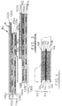
- Figure 1 of the drawings illustrates a laminate 10 in accordance with a first preferred embodiment of the present invention.
- the laminate 10 is intended for use in forming security enclosures, such as described in the abovementioned U.K. patent application No. 2220513A.
- the laminate 10 comprises various layers which are intended to provide an indication if any attempt is made to penetrate the laminate in order to gain access to material or objects contained within an enclosure formed using the laminate.
- the laminate 10 can be thought of as comprising two portions 12, 14 and the present invention relates to improvements to the upper portion 12 (as seen in Figure 1), while the lower portion 14 is similar to the corresponding portion of the laminate described in the above mentioned U.K. patent application.
- the upper portion 12 comprises a flexible sheet of insulating material which will normally be provided in the form of a thin insulating film 16.
- Lines 18, 20 of electrically responsive material, preferably semi-conductive material are printed on both sides of the film 16.
- the lines 18, 20 preferably extend diagonally over the film 16 and are formed of semi-conductive ink, most preferably comprising a matrix of low molecular weight polyester resin filled with carbon and graphite.
- each line may be formed with a resistivity of 6 ohms - cm for 25% carbon loading in polyester and is applied by screen printing to a dry thickness of approximately 10 microns.
- the lines 18, 20 are spaced to produce a matrix of diamond shaped areas of no larger dimensions than 10 millimetres,
- the matrix of lines 18, 20 forms a continually connected circuit which will be broken if attempts are made to penetrate the film by cutting, abrasion, application of solvent, or application of heat.
- second and third layers of insulating material in the form of films 22, 24 are adhered to and cover the respective lines.
- the second insulating film 22 will form the outer surface of the enclosure.
- the insulating films 22, 24 are secured by means of layers 26, 28, 30 of adhesive, as will be described in more detail. It will also be noted that there is a further layer 32 between the insulating film 16 and the semi-conductive lines 18, which will also be described in more detail.
- the second portion 14 of the laminate comprises two layers 36, 38 of semi-conductive fibrous material separated by a layer 40 of thin insulating film.
- Each semi-conductive layer 36, 38 is made throughout of fibrous material such that, in use, if a sharp object penetrates the layers, the object will pull fragments of the upper semi-conductive layer 36 through the intervening insulating layer 40 to touch, and make electrical contact with, the lower semi-conductive layer 38.
- the insulating layer should be thinner than the length of the conductive fibres produced by pushing an object through one of the semi-conductive layers 36, 38.
- the insulating layer 40 should therefore be no thicker than, and preferably is thinner than, the semi-conductive layers 36, 38.
- the preferred semi-conductive fibrous material is low densified conductive polytetrafluoroethylene (PTFE) having a volume resistivity typically from 1 to 10 ohms - cm and the preferred insulating material is polyester film, around 12 microns thick.
- PTFE conductive polytetrafluoroethylene
- Fig 1 also shows patterned adhesive layers 42, 44 between the insulating film layer 40 and the semi-conductive fibrous layers 36, 38.
- the two portions 12, 14 are joined together by means of a layer of adhesive 49.
- the laminate 10 may be folded or formed into an enclosure and various ones of the layers of the laminate are connected to means for detecting changes in the electrical characteristics of the layers, in the form of a monitoring device 50.
- a monitoring device 50 will typically maintain the lines 18, 20 and semi-conductive layers 36, 38 at reference potentials. Thus, any break or damage to the lines 18, 20 caused by penetration of the upper portion 12 will result in a detectable change in the potential of the lines. Similarly, penetration of the semi-conductive fibrous layers 36, 38 by an object will result in electrical connection between the layers and thus also produce a detectable change in the potential of the layers 36, 38.
- the monitoring device 50 On detecting an attempt to penetrate the enclosure the monitoring device 50 produces an output signal which may, for example, activate an alarm or destroy or erase information contained in or on objects contained within the enclosure.
- An unauthorised entry to the enclosure may include an attempt to separate the layers of the laminate, and in particular to separate the layers to reveal the semi-conductive lines 18, 20 so that, for example, attempts can be made to isolate particular lines from the monitoring device 50 to allow them to be cut through or removed. This would typically involve an attempt to peel back the outermost insulating film 22 and it is to this method of gaining entry that this invention particularly relates.
- a low tensile strength layer 32 having lower cohesion than adhesion is printed on at least the top side of the film 16.
- the material for the layer has considerably lower cohesion than adhesion.
- the layer 32 may comprise an ethylvinyl acetate (EVA) having high vinyl acetate (VA) content, for example 70% VA, also filled to 45%-60% (by weight EVA) with fumed silica (typically having particle size of 12 nm and 20 m 2 /g surface area). It is also preferred that the material contains a black pigment such that the carbon loaded semi-conductive lines 18 are not easily visible on the layer 32.
- EVA ethylvinyl acetate
- VA vinyl acetate
- fumed silica typically having particle size of 12 nm and 20 m 2 /g surface area
- the two layers of adhesive 26, 28 become homogeneous after a time, typically one or two days.
- the lines 18 are effectively sandwiched and supported between two layers of adhesive, in this particular example the adhesive layers 28, 32 being of EVA and one being filled with fumed silica to reduce its tensile strength. In practise, the adhesive will flow to occupy the air gaps which may be seen between the lines 18 in the Figure. Also, it should be noted that the thickness of the adhesive layers shown in the Figures is somewhat exaggerated.
- the materials which form the adhesive layers 26, 28 and the low tensile strength layer 32 and the matrix material of the lines 18 are selected such that the lines 28 and the other layers are chemically different such that only moderate carbon migration takes place from the lines 18 to the layers 26, 28, 30 and 32. Such migration results in a slight but acceptable rise in electrical resistance of the lines 18.
- the resulting laminate is robust in normal use and may be folded and creased without track damage.
- Figure 2 of the drawings illustrates a laminate in accordance with a second preferred embodiment of the present invention.
- the laminate is substantially similar to the laminate that described with reference to Figure 1 and to avoid repetition the similar features of the laminate of Figure 2 will not be described again, similar reference numerals as appeared in Figure 1 being used to indicate similar elements in Figure 2, though prefixed with a 1 in Figure 2.
- the difference between the laminates 10, 110 lies in the provision of at least one layer of fusible material between the semi-conductive fibrous layers 136, 138.
- the provision is of two layers 60, 62 of fusible material one on each side of the insulating layer 140 separating the layers 136, 138.
- the semi-conductive fusible or low melt material which forms the layers 60, 62 will melt and flow through any breaks in the insulating layer 140, to form an electrical connection between the semi-conductive layers 36, 38. This will of course affect the electrical characteristics of the layers 136, 138 and will be detected by the monitoring device 150. Details of such low melt materials are contained in our European Patent Application Serial No. 0459838.
- the upper insulating film 122a extends beyond the edge of the upper portion 112a to form a flap A.
- the underside of the flap A is provided with adhesive layer 126a, which is utilised to secure the flap A to the other edge portion.
- the lower portion 114a does not extend to the edge of the upper portion 112a and at the "exposed" inner face of the portion 112a, an edge layer of low tensile strength material 133a is provided below the conductive lines 120a.
- An additional layer of adhesive 70a is provided over the exposed lines 120a and continues over the edge of the inner face of the lower portion 114a.
- the upper insulating film 122b does not extend to the edge of the laminate, leaving a portion of the adhesive layer 128b exposed.
- a further layer of adhesive 70b is provided on the edge of the film 122b.
- Figure 4 which illustrates the edge configuration of the lower portion 114 for forming both upper and lower overlapping parts
- the various insulating layers 124, 140, 146 are simply extended relative to the semi-conductive layers 136, 138 to ensure there is no contact between the layers 136, 138 at the edges.
- edges of the laminate are brought together in the relative overlapping positions shown in Figure 3 and the various layers of adhesive 126a, 70a, 128b, 70b which come into contact become homogeneous over a period of time to provide a secure join. If any attempt is made to separate the edges, as the outer insulating film 122a, or any of the other layers is peeled back, one or more of the low tensile strength layers 132a, 133a, 132b will fragment, breaking the lines 118a, 120a, 118b.
Landscapes
- Engineering & Computer Science (AREA)
- Computer Hardware Design (AREA)
- General Engineering & Computer Science (AREA)
- Physics & Mathematics (AREA)
- General Physics & Mathematics (AREA)
- Laminated Bodies (AREA)
- Burglar Alarm Systems (AREA)
- Packaging For Recording Disks (AREA)
- Casings For Electric Apparatus (AREA)
- Electrical Discharge Machining, Electrochemical Machining, And Combined Machining (AREA)
Description
Claims (12)
- A security enclosure comprising a first layer (16) of an insulating material extending over the whole of the area of the enclosure and carrying a linear electrically responsive element (18) on at least one surface thereof, a low tensile strength layer (32) having lower cohesion than adhesion located between the first layer (16) of insulating material and the electrically responsive element (18) and a second layer (22) of insulating material adhered to and covering the electrically responsive element (18), the element (18) being arranged in a configuration on the surface of the first layer (16) so dividing the surface that attempted penetration of the enclosure changes an electrical characteristic of the element (18), and detection means (50) being provided for detecting said change, an attempt to remove the second layer (22) of insulating material to gain access to the element (18) resulting in breakup of the low tensile strength layer (32) and thus damaging the element (18) to produce a detectable change in said electrical characteristic of the element (18).
- The security enclosure of claim 1 wherein the first and second layers (16, 22), the low tensile strength layer (32) and the electrically responsive element (18) are flexible to allow the laminate to be folded and creased.
- The security enclosure of claim 1 or claim 2 wherein the linear electrically responsive element (18) is a carrier filled with conductive material.
- The security enclosure of claim 3 wherein the linear electrically responsive element (18) is a first polymer filled with carbon or graphite.
- The security enclosure of claim 4 wherein the low tensile strength layer (32) is a second polymer and an adhesive (26, 28) provided between the second layer (22) of insulating material and the element (18) is a third polymer and said polymers are selected to minimise migration of conductive material from the first polymer to the second and third polymers.
- The security enclosure of any one of claims 3, 4 or 5 wherein the electrically responsive element (18) is a semi-conductive ink comprising a matrix of low molecular weight polyester resin filled with carbon and graphite.
- The security enclosure of any one of claims 1 through 6 wherein the low tensile strength layer (32) is a polymer filled with granular material.
- The security enclosure of claim 7 wherein the low tensile strength layer (18) is an ethyl vinyl acetate having high vinyl acetate content and filled to 45% to 60% by weight of fumed silica.
- The security enclosure of any one of claims 1 through 8 wherein the other surface of the first layer (16) of insulating material carries a further linear electrically responsive element (20) and a third layer (24) of insulating material is adhered to and covers the further element (20), the electrically responsive elements (18, 20) being in the form of lines and the lines on one side of the first layer (16) extending obliquely relative to the lines on the other side and being connected thereto at edge portions of the first layer (16) to form at least one conductor so dividing the first layer (16) into a number of relatively small areas that attempted penetration of the enclosure changes an electrical characteristic of said at least one conductor.
- The security enclosure of claim 9 wherein the layers define a laminate which is folded and joined at overlapping edge portions to define the enclosure and the lines (118b, 120a) at at least one of the overlapping edges of the laminate are exposed beyond an adjacent edge of the respective insulating layer (122b, 124), and a layer (132b, 133a) of low tensile strength material is provided between the first layer of insulating material (116) and the lines of electrically responsive material (118b, 120a) at said at least one of the overlapping edges so that any attempt to separate the overlapping edges to gain access to the enclosure results and breakup of the low tensile strength layer (132b, 133a) and damage to the lines (118b, 120a).
- A laminate for use in forming a security enclosure, the laminate (10) comprising a first layer of an insulating material (16) carrying a linear electrically responsive element (18, 20) on at least one surface thereof, a layer of low tensile strength material (32) having lower cohesion than adhesion being located between the first layer of insulating material (16) and the electrically responsive element (18), a second layer of insulating material (22) being adhered to and covering the electrically responsive element (18), the element (18) being arranged in a configuration on the surface so dividing the surface that attempted penetration of the laminate (10) changes an electrical characteristic of the element (18), which change may be detected by an appropriate electrical circuit and an attempt to remove the second layer (22) of insulating material to gain access to the linear electrically responsive element (18) will result in breakup of the low tensile strength layer (32) and thus damage the element (18) and produce a detectable change in said electrical characteristic of the element (18).
- A security enclosure comprising a flexible laminate (64) which is folded and joined at overlapping edge portions to define the enclosure, the laminate (64) comprising a flexible first layer of insulating material (116) extending over the whole of the area of the enclosure and carrying lines of electrically responsive material (120) on one side thereof, a further layer of insulating material (124) being adhered to and covering the lines (120) with the lines (120a) at at least one of the overlapping edges of the laminate being exposed beyond and adjacent edge of the insulating layer (124), the lines (120) being arranged in a configuration on the surface so dividing the laminate that attempted penetration of the enclosure changes an electrical characteristic of the lines (120), means (50) being provided for detecting said changes in the electrical characteristics of the lines (120) and a layer of low tensile strength material (133a) being provided between the first layer of insulating material (116) and the lines of electrical responsive material (120a) at said at least one of the overlapping edges, the low tensile strength material having lower cohesion than adhesion and any attempt to separate the overlapping edges to gain access to the enclosure resulting in breakup of the low tensile strength layer (133a) and damage to the lines (120a) to produce said detectable change.
Applications Claiming Priority (2)
| Application Number | Priority Date | Filing Date | Title |
|---|---|---|---|
| GB9113437 | 1991-06-21 | ||
| GB919113437A GB9113437D0 (en) | 1991-06-21 | 1991-06-21 | Improvements in security enclosures |
Publications (3)
| Publication Number | Publication Date |
|---|---|
| EP0526972A2 EP0526972A2 (en) | 1993-02-10 |
| EP0526972A3 EP0526972A3 (en) | 1993-10-06 |
| EP0526972B1 true EP0526972B1 (en) | 1998-03-04 |
Family
ID=10697091
Family Applications (1)
| Application Number | Title | Priority Date | Filing Date |
|---|---|---|---|
| EP92305197A Expired - Lifetime EP0526972B1 (en) | 1991-06-21 | 1992-06-05 | Improvements in security enclosures |
Country Status (8)
| Country | Link |
|---|---|
| US (1) | US5289785A (en) |
| EP (1) | EP0526972B1 (en) |
| JP (1) | JP3366666B2 (en) |
| DE (1) | DE69224567T2 (en) |
| DK (1) | DK0526972T3 (en) |
| ES (1) | ES2114915T3 (en) |
| GB (2) | GB9113437D0 (en) |
| NO (1) | NO305817B1 (en) |
Families Citing this family (36)
| Publication number | Priority date | Publication date | Assignee | Title |
|---|---|---|---|---|
| GB2270785B (en) * | 1992-09-22 | 1996-05-08 | Gore & Ass | Improvements in security enclosure manufacture |
| GB2297540B (en) * | 1993-03-12 | 1997-01-29 | Gore & Ass | Tamper respondent enclosure |
| FR2730088B1 (en) * | 1995-01-26 | 1997-04-18 | Plastiques Franc Des | PLASTIC CASE, ESPECIALLY FOR A COMPACT DISC |
| US6667004B2 (en) | 1995-01-26 | 2003-12-23 | La Francaise Des Plastiques | Method of forming a box or box element of plastic material |
| AU5535896A (en) * | 1995-04-06 | 1996-10-23 | Regents Of The University Of California, The | Puncture detecting barrier materials |
| DE19600770C2 (en) * | 1996-01-11 | 1997-11-13 | Ibm | Security film with EMC protection |
| US5681122A (en) * | 1996-02-20 | 1997-10-28 | Ncr Corporation | Fluid isolation and dispersion system for tactile input devices |
| US5802459A (en) * | 1996-02-20 | 1998-09-01 | Ncr Corporation | Peripheral device having a communication port for cable or wireless module connection |
| US5686909A (en) * | 1996-06-05 | 1997-11-11 | Steinhauser; Louis P. | Alarm system for boat covers and automobile convertible tops |
| IL119509A (en) * | 1996-10-28 | 2000-02-17 | Hi G Tek Ltd | Electronic tag |
| GB9712145D0 (en) | 1997-06-12 | 1997-08-13 | Gore W L & Ass Uk | Folding apparatus |
| EP0955616A1 (en) * | 1998-05-07 | 1999-11-10 | Hi-G-Tek Ltd | Electronic tag |
| US6097482A (en) * | 1999-06-08 | 2000-08-01 | Philip Morris Incorporated | High speed flaw detecting system for reflective material |
| US6268567B1 (en) | 2000-01-25 | 2001-07-31 | International Business Machines Corporation | Dual purpose ribbon cable |
| US6597283B2 (en) * | 2000-05-02 | 2003-07-22 | Hard 2 Top Products, Inc. | Protective cover assembly |
| NO312373B1 (en) * | 2000-06-29 | 2002-04-29 | Kjell Birkeland | Wall construction, especially for a valuables storage box, as well as the use of such a wall structure sometimes sidewalls in a storage box |
| US6982642B1 (en) | 2000-11-20 | 2006-01-03 | International Business Machines Corporation | Security cloth design and assembly |
| SE524753C2 (en) * | 2002-02-06 | 2004-09-28 | Sqs Ab | Method and apparatus for containers |
| GB2412996B (en) | 2004-04-08 | 2008-11-12 | Gore & Ass | Tamper respondent covering |
| JP4879174B2 (en) * | 2004-07-14 | 2012-02-22 | ジェイ.ダー ハビッブ | Composite container for preventing tampering that incorporates equipment related to the application |
| US7323986B2 (en) | 2004-09-03 | 2008-01-29 | Gore Enterprise Holdings, Inc. | Reusable tamper respondent enclosure |
| US7015823B1 (en) * | 2004-10-15 | 2006-03-21 | Systran Federal Corporation | Tamper resistant circuit boards |
| US7736710B2 (en) * | 2005-08-01 | 2010-06-15 | Stora Enso Ab | Package and method of closing and opening a package |
| EP1912872A1 (en) * | 2005-08-01 | 2008-04-23 | Stora Enso Ab | A package |
| US8487763B2 (en) * | 2006-10-06 | 2013-07-16 | University Of Maine System Board Of Trustees | Breach detection system for containers |
| US7760086B2 (en) | 2006-11-03 | 2010-07-20 | Gore Enterprise Holdings, Inc | Tamper respondent sensor and enclosure |
| US7799394B2 (en) * | 2006-11-14 | 2010-09-21 | Millercoors, Llc | Container with insulative label |
| US20080278353A1 (en) * | 2007-05-11 | 2008-11-13 | Measurement Specialties, Inc. | Tamper resistant electronic transaction assembly |
| US7787256B2 (en) | 2007-08-10 | 2010-08-31 | Gore Enterprise Holdings, Inc. | Tamper respondent system |
| US8344885B2 (en) * | 2008-01-22 | 2013-01-01 | Angel Secure Networks Inc. | Container with interior enclosure of composite material having embedded security element |
| US8698627B2 (en) * | 2009-01-07 | 2014-04-15 | Meadwestvaco Corporation | Security packaging |
| US8836509B2 (en) * | 2009-04-09 | 2014-09-16 | Direct Payment Solutions Limited | Security device |
| US8669886B2 (en) * | 2010-10-28 | 2014-03-11 | Xac Automation Corp. | Data entry module |
| DE102010054683A1 (en) * | 2010-12-14 | 2012-06-14 | Sächsisches Textilforschungsinstitut e.V. | Security packer |
| CN103538776B (en) * | 2013-10-22 | 2016-06-08 | 浙江纺织服装职业技术学院 | A kind of antitheft printing bag of logistics |
| CN105962652A (en) * | 2016-04-22 | 2016-09-28 | 杜方兴 | Novel account book storage device |
Family Cites Families (19)
| Publication number | Priority date | Publication date | Assignee | Title |
|---|---|---|---|---|
| BE665729A (en) * | 1964-07-01 | 1900-01-01 | ||
| US3594770A (en) * | 1968-10-28 | 1971-07-20 | Lewis Eng Co | Printed-circuit type security apparatus for protecting areas |
| AT315019B (en) * | 1971-02-23 | 1974-05-10 | Gao Ges Automation Org | Security container or the like. |
| US3925584A (en) * | 1972-08-24 | 1975-12-09 | Daiichi Seiyaku Co | Adhesive seal and tape for sealing |
| US4000488A (en) * | 1974-04-19 | 1976-12-28 | Bernard Ephraim | Label alarm system |
| WO1983000246A1 (en) * | 1981-07-06 | 1983-01-20 | Jorgensen, Poul, Richter | Alarm system for safeguarding against the breakthrough of a surface |
| GB2209618B (en) * | 1986-05-03 | 1991-01-09 | Adrian Francis Wolf | Alarm system |
| EP0260330A1 (en) * | 1986-09-13 | 1988-03-23 | Tele-Security-Foto Überwachungsanlagen GmbH | Theft protection for objects |
| US4749084A (en) * | 1986-11-12 | 1988-06-07 | Minnesota Mining And Manufacturing Co. | Tamper-indicating package with randomly disposed filaments |
| US4954185A (en) * | 1987-01-14 | 1990-09-04 | Kollmorgen Corporation | Method of applying adherent coating on copper |
| JPS63274196A (en) * | 1987-05-06 | 1988-11-11 | Mitsubishi Electric Corp | Metal core printed circuit board |
| EP0303225A3 (en) * | 1987-08-10 | 1990-01-10 | Kashima Industries, Co. | Epoxy resin film covered with metal foil and flexible printed wiring board |
| US4754629A (en) * | 1987-11-10 | 1988-07-05 | Allen Mark L | Safe relocking system |
| DE3743780A1 (en) * | 1987-12-23 | 1989-07-06 | Bayer Ag | METHOD FOR IMPROVING THE ADHESIVITY OF CURRENTLY DEPOSITED METAL LAYERS ON POLYIMIDE SURFACES |
| GB8814471D0 (en) * | 1988-06-17 | 1988-07-20 | Gore & Ass | Security enclosure |
| US4985294A (en) * | 1988-08-25 | 1991-01-15 | The Yokohama Rubber Co., Ltd. | Printed wiring board |
| GB9012272D0 (en) * | 1990-06-01 | 1990-07-18 | Gore W L & Ass Uk | Flexible sheeting |
| GB9113455D0 (en) * | 1991-06-21 | 1991-08-07 | Gore W L & Ass Uk | Improvements in security enclosures |
| US10234158B2 (en) * | 2017-03-06 | 2019-03-19 | Mitsubishi Electric Research Laboratories, Inc. | Coordinated operation of multiple space-conditioning systems |
-
1991
- 1991-06-21 GB GB919113437A patent/GB9113437D0/en active Pending
-
1992
- 1992-06-05 EP EP92305197A patent/EP0526972B1/en not_active Expired - Lifetime
- 1992-06-05 DE DE69224567T patent/DE69224567T2/en not_active Expired - Lifetime
- 1992-06-05 ES ES92305197T patent/ES2114915T3/en not_active Expired - Lifetime
- 1992-06-05 GB GB9211963A patent/GB2256958B/en not_active Revoked
- 1992-06-05 DK DK92305197T patent/DK0526972T3/en active
- 1992-06-18 US US07/900,866 patent/US5289785A/en not_active Expired - Lifetime
- 1992-06-19 NO NO922450A patent/NO305817B1/en not_active IP Right Cessation
- 1992-06-22 JP JP16280092A patent/JP3366666B2/en not_active Expired - Lifetime
Also Published As
| Publication number | Publication date |
|---|---|
| ES2114915T3 (en) | 1998-06-16 |
| DE69224567T2 (en) | 1998-09-17 |
| NO922450L (en) | 1992-12-22 |
| NO922450D0 (en) | 1992-06-19 |
| GB9113437D0 (en) | 1991-08-07 |
| EP0526972A2 (en) | 1993-02-10 |
| JP3366666B2 (en) | 2003-01-14 |
| DK0526972T3 (en) | 1998-09-28 |
| EP0526972A3 (en) | 1993-10-06 |
| NO305817B1 (en) | 1999-07-26 |
| GB2256958A (en) | 1992-12-23 |
| GB9211963D0 (en) | 1992-07-15 |
| JPH05201483A (en) | 1993-08-10 |
| GB2256958B (en) | 1994-11-16 |
| DE69224567D1 (en) | 1998-04-09 |
| US5289785A (en) | 1994-03-01 |
Similar Documents
| Publication | Publication Date | Title |
|---|---|---|
| US5289785A (en) | Security enclosures | |
| EP0663096B1 (en) | Improvements in security enclosure manufacture | |
| US4972175A (en) | Security enclosures | |
| EP1023707A1 (en) | Tamper respondent enclosure | |
| TWI617943B (en) | Safety device with tearable substrate | |
| EP0526066B1 (en) | Improvements in security enclosures | |
| EP0540139B1 (en) | Improvements in security enclosures | |
| GB2504478A (en) | Security Wrap Film for Protecting Electronic Device | |
| US20180124915A1 (en) | Tamper-respondent assemblies with trace regions of increased susceptibility to breaking | |
| EP0526971A2 (en) | Improvement in security enclosures | |
| GB2330439A (en) | Tamper respondent enclosure | |
| GB2254720A (en) | Security enclosure |
Legal Events
| Date | Code | Title | Description |
|---|---|---|---|
| PUAI | Public reference made under article 153(3) epc to a published international application that has entered the european phase |
Free format text: ORIGINAL CODE: 0009012 |
|
| AK | Designated contracting states |
Kind code of ref document: A2 Designated state(s): DE DK ES FR GB IT SE |
|
| PUAL | Search report despatched |
Free format text: ORIGINAL CODE: 0009013 |
|
| AK | Designated contracting states |
Kind code of ref document: A3 Designated state(s): DE DK ES FR GB IT SE |
|
| 17P | Request for examination filed |
Effective date: 19940318 |
|
| GRAG | Despatch of communication of intention to grant |
Free format text: ORIGINAL CODE: EPIDOS AGRA |
|
| 17Q | First examination report despatched |
Effective date: 19970414 |
|
| GRAG | Despatch of communication of intention to grant |
Free format text: ORIGINAL CODE: EPIDOS AGRA |
|
| GRAH | Despatch of communication of intention to grant a patent |
Free format text: ORIGINAL CODE: EPIDOS IGRA |
|
| GRAH | Despatch of communication of intention to grant a patent |
Free format text: ORIGINAL CODE: EPIDOS IGRA |
|
| GRAA | (expected) grant |
Free format text: ORIGINAL CODE: 0009210 |
|
| AK | Designated contracting states |
Kind code of ref document: B1 Designated state(s): DE DK ES FR GB IT SE |
|
| REF | Corresponds to: |
Ref document number: 69224567 Country of ref document: DE Date of ref document: 19980409 |
|
| ITF | It: translation for a ep patent filed | ||
| ET | Fr: translation filed | ||
| REG | Reference to a national code |
Ref country code: ES Ref legal event code: FG2A Ref document number: 2114915 Country of ref document: ES Kind code of ref document: T3 |
|
| REG | Reference to a national code |
Ref country code: DK Ref legal event code: T3 |
|
| PLBE | No opposition filed within time limit |
Free format text: ORIGINAL CODE: 0009261 |
|
| STAA | Information on the status of an ep patent application or granted ep patent |
Free format text: STATUS: NO OPPOSITION FILED WITHIN TIME LIMIT |
|
| 26N | No opposition filed | ||
| REG | Reference to a national code |
Ref country code: GB Ref legal event code: IF02 |
|
| PGFP | Annual fee paid to national office [announced via postgrant information from national office to epo] |
Ref country code: DK Payment date: 20040621 Year of fee payment: 13 |
|
| PG25 | Lapsed in a contracting state [announced via postgrant information from national office to epo] |
Ref country code: DK Free format text: LAPSE BECAUSE OF NON-PAYMENT OF DUE FEES Effective date: 20050630 |
|
| REG | Reference to a national code |
Ref country code: DK Ref legal event code: EBP |
|
| PGFP | Annual fee paid to national office [announced via postgrant information from national office to epo] |
Ref country code: SE Payment date: 20110629 Year of fee payment: 20 Ref country code: FR Payment date: 20110629 Year of fee payment: 20 Ref country code: ES Payment date: 20110628 Year of fee payment: 20 |
|
| PGFP | Annual fee paid to national office [announced via postgrant information from national office to epo] |
Ref country code: GB Payment date: 20110628 Year of fee payment: 20 |
|
| PGFP | Annual fee paid to national office [announced via postgrant information from national office to epo] |
Ref country code: IT Payment date: 20110627 Year of fee payment: 20 |
|
| PGFP | Annual fee paid to national office [announced via postgrant information from national office to epo] |
Ref country code: DE Payment date: 20110629 Year of fee payment: 20 |
|
| REG | Reference to a national code |
Ref country code: DE Ref legal event code: R071 Ref document number: 69224567 Country of ref document: DE |
|
| REG | Reference to a national code |
Ref country code: DE Ref legal event code: R071 Ref document number: 69224567 Country of ref document: DE |
|
| REG | Reference to a national code |
Ref country code: GB Ref legal event code: PE20 Expiry date: 20120604 |
|
| PG25 | Lapsed in a contracting state [announced via postgrant information from national office to epo] |
Ref country code: DE Free format text: LAPSE BECAUSE OF EXPIRATION OF PROTECTION Effective date: 20120606 |
|
| REG | Reference to a national code |
Ref country code: SE Ref legal event code: EUG |
|
| PG25 | Lapsed in a contracting state [announced via postgrant information from national office to epo] |
Ref country code: GB Free format text: LAPSE BECAUSE OF EXPIRATION OF PROTECTION Effective date: 20120604 |
|
| REG | Reference to a national code |
Ref country code: ES Ref legal event code: FD2A Effective date: 20130711 |
|
| PG25 | Lapsed in a contracting state [announced via postgrant information from national office to epo] |
Ref country code: ES Free format text: LAPSE BECAUSE OF EXPIRATION OF PROTECTION Effective date: 20120606 |