EP0526334B1 - Electroless palladium plating composition - Google Patents
Electroless palladium plating composition Download PDFInfo
- Publication number
- EP0526334B1 EP0526334B1 EP92402190A EP92402190A EP0526334B1 EP 0526334 B1 EP0526334 B1 EP 0526334B1 EP 92402190 A EP92402190 A EP 92402190A EP 92402190 A EP92402190 A EP 92402190A EP 0526334 B1 EP0526334 B1 EP 0526334B1
- Authority
- EP
- European Patent Office
- Prior art keywords
- plating
- palladium
- plating composition
- hypophosphite
- composition
- Prior art date
- Legal status (The legal status is an assumption and is not a legal conclusion. Google has not performed a legal analysis and makes no representation as to the accuracy of the status listed.)
- Expired - Lifetime
Links
Images


Classifications
-
- C—CHEMISTRY; METALLURGY
- C23—COATING METALLIC MATERIAL; COATING MATERIAL WITH METALLIC MATERIAL; CHEMICAL SURFACE TREATMENT; DIFFUSION TREATMENT OF METALLIC MATERIAL; COATING BY VACUUM EVAPORATION, BY SPUTTERING, BY ION IMPLANTATION OR BY CHEMICAL VAPOUR DEPOSITION, IN GENERAL; INHIBITING CORROSION OF METALLIC MATERIAL OR INCRUSTATION IN GENERAL
- C23C—COATING METALLIC MATERIAL; COATING MATERIAL WITH METALLIC MATERIAL; SURFACE TREATMENT OF METALLIC MATERIAL BY DIFFUSION INTO THE SURFACE, BY CHEMICAL CONVERSION OR SUBSTITUTION; COATING BY VACUUM EVAPORATION, BY SPUTTERING, BY ION IMPLANTATION OR BY CHEMICAL VAPOUR DEPOSITION, IN GENERAL
- C23C18/00—Chemical coating by decomposition of either liquid compounds or solutions of the coating forming compounds, without leaving reaction products of surface material in the coating; Contact plating
- C23C18/16—Chemical coating by decomposition of either liquid compounds or solutions of the coating forming compounds, without leaving reaction products of surface material in the coating; Contact plating by reduction or substitution, e.g. electroless plating
- C23C18/31—Coating with metals
- C23C18/42—Coating with noble metals
- C23C18/44—Coating with noble metals using reducing agents
Definitions
- the present invention relates to a composition for electroless palladium plating.
- noble metals or alloys thereof are stable in electrical characteristics and highly resistant to corrosion and abrasion, they have been widely used, for example as materials for contacts of electronic components.
- noble metals are chiefly used for electroplating, particularly gold electroplating, the gold plating involving high costs.
- High density surface mounting technology is the mainstream in the field of printed board production.
- a surface mounted substrate is generally prepared by plating a copper circuit with gold.
- gold plating diffuses with copper in soft soldering, the copper circuit must be pretreated with electroless nickel plating, which leads to complicated preparation process and lower productivity.
- the use of palladium electroplating in place of gold electroplating is on the increase.
- compositions widely used for electroless palladium plating are, for example, a composition comprising a bivalent palladium salt, ammonia, ethylenediaminetetraacetate salt and hydrazine and a composition comprising a bivalent palladium salt, ethylenediamine, ethylenediaminetetraacetate salt and sodium hypophosphite (disclosed in Japanese Examined Patent Publication No. 26764/1971).
- these plating compositions are unstable in baths and decomposed in a short period of time.
- methods comprising adding a bivalent sulfur-containing organic compound have been proposed in Japanese Examined Patent Publications No. 37045/1978 and Japanese Unexamined Patent Publication No. 124280/1987, etc.
- GB-A-1 164 776 discloses an electroless palladium plating composition
- a palladium compound at least one member selected from the group consisting of ammonia and saturated alkylamine compounds, a hypophosphite reducing agent and which composition is preferably used in a pH-range of 8 to 11.
- the purpose of the present invention is to provide a composition for electroless palladium plating which can be used in an industrial scale.
- an electroless palladium composition containing high-molecular weight polyethyleneimine having molecular weight of 300 to 100,000 and unsaturated alkylamine exhibits a good bath stability and enables the formation of a uniform, minute and close palladium plating while suppressing or preventing the occurrence of internal stress in the plating.
- the present invention has been accomplished based on this novel finding.
- the present invention provides an electroless palladium plating composition which comprises (1) 0.001-0.1 mol/l of a palladium compound, (2) 0.01-1 mol/l of a hypophosphite compound, (3) 0.01-5 mol/l of at least one member selected from the group consisting of ammonia and saturated alkylamine compounds, (4) 0.01-20 mg/l of high-molecular weight polyethyleneimine having molecular weight of 300 to 100,000 and (5) 0.01-10 g/l of unsaturated alkylamine, and which is used at a pH in the range of 5-10.
- Examples of palladium compounds useful in the invention include known compounds such as palladium oxide, palladium chloride, palladium nitrate, palladium acetate, sodium palladium chloride, potassium palladium chloride, ammonium palladium chloride, palladium sulfate, tetraammine palladium chloride, dinitrodiammine palladium and like palladium compounds.
- the concentration of the palladium compound in the plating composition of the invention is in the range of 0.001 to 0.1 mol/l, preferably 0.003 to 0.05 mol/l. When the concentration is lower than 0.001 mol/l, the deposition rate is lowered and thus leads to lower productivity, whereas when the concentration is higher than 0.1 mol/l, the plating composition becomes unstable, hence undesirable.
- hypophosphite compounds useful in the invention include known compounds such as hypophosphorous acid, ammonium hypophosphite, potassium hypophosphite, sodium hypophosphite, lithium hypophosphite, calcium hypophosphite.
- the hypophosphite compound acts as a reducing agent for palladium ions in the plating composition of the invention.
- the concentration of the hypophosphite compound in the plating composition of the invention is in the range of 0.01 to 1 mol/l, preferably 0.05 to 0.5 mol/l. When the concentration is lower than 0.01 mol/l, the deposition rate is lowered, whereas when the concentration is higher than 1 mol/l, the plating composition becomes unstable, hence undesirable.
- saturated alkylamine compounds for use in the invention include widely used compounds; such as methylamine, ethylamine, propylamine, dimethylamine, trimethylamine, methylethylamine, isopropylamine; methylenediamine, ethylenediamine, propylenediamine, butylenediamine; dimethylenetriamine, diethylenetriamine, triethylenetetramine, tetraethylenepentamine, pentaethylenehexamine; ethylenediaminetetraacetic acid, diethylenetriaminepentacetic acid, N-hydroxyethylethylenediaminetriacetic acid, nitrilotriacetic acid and alkali metal salts thereof; glycine, N-methylglycine.
- At least one member selected from the group consisting of saturated alkylamine compounds and ammonia is added to the plating composition so that palladium-complexes can be formed to stabilize palladium in the plating solution.
- the concentration of the saturated alkylamine compound and ammonia in the plating composition of the invention is in the range of 0.01 to 5 mol/l, preferably 0.05 to 3 mol/l.
- the use of the saturated alkylamine compound in a concentration lower than 0.01 mol/l makes the plating composition unstable, whereas the use thereof in a concentration higher than 5 mol/l stabilizes the plating composition but lowers the deposition rate and increases costs, hence undesirable.
- At least two compounds selected from ammonia and saturated alkylamine compounds can be used in combination insofar as total concentration thereof is within the above-mentioned range.
- High-molecular weight polyethyleneimine to be used in the invention has a molecular weight of 300 to 100,000 (polymerization degree 8 to 2350), preferably 600 to 70,000 (polymerization degree 14 to 1600).
- Polyethyleneimine having a molecular weight of less than 300 has an insufficient effect on the stabilization of the plating composition, whereas polyethyleneimine having a molecular weight of more than 100,000 makes the plating composition so stable as to lower the deposition rate, hence undesirable.
- High-molecular weight polyethyleneimine of the invention may be a complete linear polymer or a polymer containing tertiary amine which branches off at nitrogen in the molecule. These polymers can be used simply or in combination thereof.
- the concentration of the high-molecular weight polyethyleneimine in the plating composition of the invention is in the range of 0.01 to 20 mg/l.
- the use of the polyethyleneimine in a concentration lower than 0.01 mg/l produces an insufficient effect on the stabilization of the plating composition, whereas the use thereof in a concentration higher than 20 mg/l lowers the deposition rate, hence undesirable.
- unsaturated alkylamines useful in the invention include known compounds such as monoethynylamine, diethynylamine, monovinylamine, divinylamine, monoallylamine, diallylamine, propenylamine, isopropenylamine, aniline; N-monoethynylethylenediamine, N-monovinylethylenediamine, N-monoallylethylenediamine, N,N'-diallylethylenediamine, N-isopropenylethylenediamine, N-phenylethylenediamine ; N-allyldiethylenetriamine, N,N'-diallyldiethylenetriamine, N-vinyltriethylenetetramine.
- the concentration of the unsaturated alkylamine in the plating composition of the invention is in the range of 0.01 to 10 g/l, preferably 0.1 to 5 g/l.
- the use of unsaturated alkylamine in a concentration lower than 0.01 g/l produces an insufficient effect on the stabilization of the plating composition, whereas the use thereof in a concentration higher than 10 g/l contributes to stabilization of the plating composition but is uneconomical. Therefore, the concentration of lower than 0.01 g/l or higher than 10 g/l is undesirable.
- the unsaturated alkylamine of the invention may be partially hydrolyzed into an amine and an aldehyde or a ketone compound in the plating composition.
- An electroless palladium plating composition of the invention comprising said ingredients is usually usable at a wide range of temperature, i.e., 25 to 80°C, preferably 35 to 70°C.
- temperature i.e. 25 to 80°C, preferably 35 to 70°C.
- the temperature is lower than 25°C, the deposition rate is lowered, hence not practical.
- the temperature is higher than 80°C, the deposition rate is increased but the plating composition becomes unstable, hence undesirable.
- the plating composition of the invention is used at a pH in the range of 5 to 10, preferably 5.5 to 9.
- a pH in the range of 5 to 10, preferably 5.5 to 9.
- the pH of the plating composition can be adjusted by a usual method using an acid solution such as hydrochloric acid and sulfuric acid or an alkaline solution such as sodium hydroxide.
- an electroless palladium plating composition of the invention When an electroless palladium plating composition of the invention is applied to metals such as Fe, Ni, Au, Ag, Pt, Ru, Rh and Pd or alloys thereof, a plating layer is autocatalytically deposited on the metals or alloys by simply immersing them in the plating composition.
- a plating layer When the composition is applied to non-catalytic materials such as resins, ceramics and glasses, the materials are catalyzed by a sensitizing-activating method or characterizing-accelerating method to autocatalytically deposit a plating layer on the materials.
- Electroless palladium plating composition of the invention has the following excellent properties.
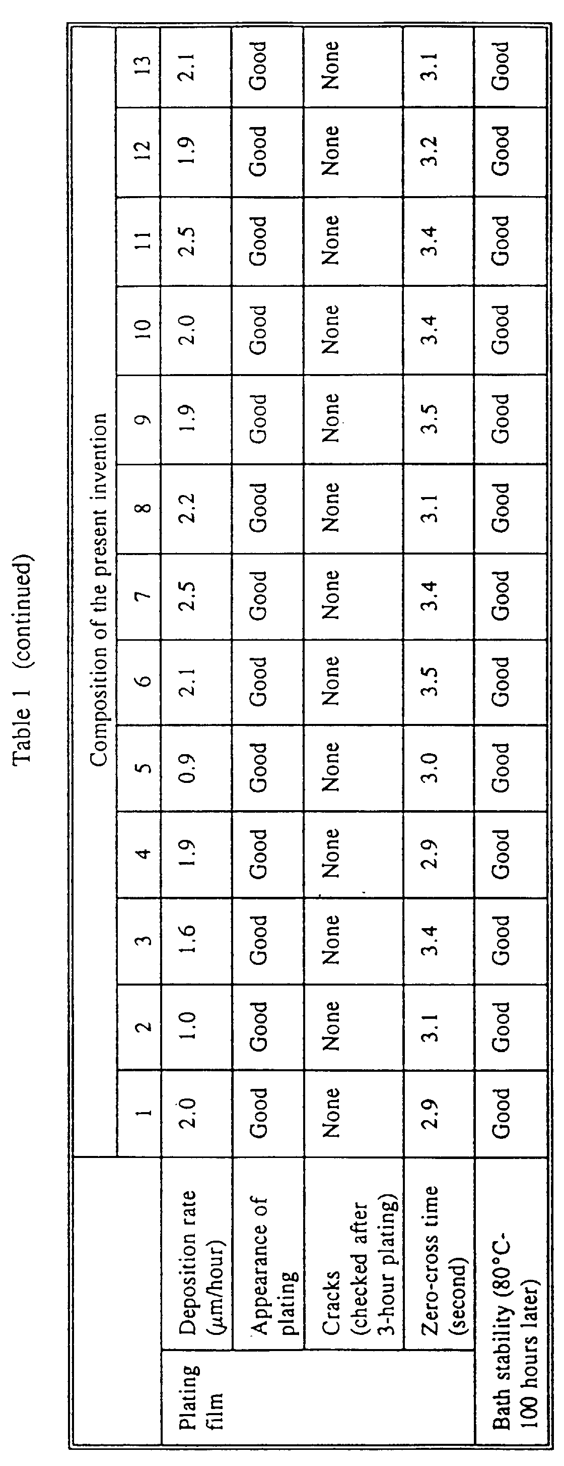
- Plating compositions of the invention (Nos.1-13) were prepared by incorporating ingredients in the ratios given in Table 1 and placed in baths. Plating was carried out in each of the plating baths and the films formed and baths were evaluated. The results are shown in Table 1.
- Copper sheets (2 cm x 2 cm x 0. 03 cm) were used as substrates for plating.
- Plating treatment consists of the following steps. Copper sheets were immersed in an aqueous solution of 50 g/l of an alkali degreasing agent (trademark “OPC-250 Cleaner M", product of Okuno Chemical Industry Co., Ltd.) at 60°C for 5 minutes for degrease of the copper plate, then washed with water, further immersed in an aqueous solution of 200 ml/l of an activating reagent (trademark "ICP Accera", product of Okuno Chemical Industry Co., Ltd.) at 25°C for 1 minute for activation of the copper plate, thereafter washed with water and finally immersed in 1l of respective plating compositions (Nos.1-13) to carry out plating.
- the copper sheets were rocked with an amplitude of 5 cm at the speed of 2 m/min for agitation during plating treatment.
- Solderability of each plating was evaluated according to a usual menisco-graph method. Stated more specifically, copper sheet test pieces (1 cm x 5 cm x 0.03 cm) were subjected to the foregoing electroless palladium plating treatment to form films of 1 ⁇ m thickness thereon and then immersed in rosin flux (a solution of 350 g of resin in 1l of isopropyl alcohol) for 10 seconds. Subsequently, using a solder checker (product of Lesca Co.
- the occurrence of cracks was determined by examining the films formed by three consecutive hour plating under an electron microscope with a magnification of 4,000.
- the films formed had nice gloss and exhibited a good adhesion property in a folding test. After three consecutive hour plating, the plating films kept glossy and no cracks were observed under the electron microscope. Furthermore, the stability of the plating baths did not change, i.e., the plating compositions were stable. In contrast, when compositions Nos.14-21 were used, all the plating baths except sulfuric additive-containing ones showed insufficient stability, i.e., all decomposed when they were allowed to stand at 80°C for 100 hours. Although the sulfuric additive-containing plating baths were stable, cracks were observed in the films when plating continued for three hours.
- Example 1 The same electroless palladium plating composition as in Example 1 (No.1 in Table 1) was used to form thick electroless palladium plating films. Copper sheets (2 cm x 2 cm x 0.03 cm) were used as test pieces. The same plating treatment and conditions as in Example 1 were used except that the plating baths were divided in two and kept one at 50°C and the other at 60°C. The results are shown in Figure 1.
- electroless palladium plating films were formed on four different materials other than copper: a steal plate, an electroless nickel-plated plate, ABS resin and alumina ceramics.
- graphs show the relation between plating time and thickness of the plating layer deposited on each substrate material.
- a cold rolled steel plate (2 cm x 5 cm x 0.03 cm) was used as a substrate and first degreased by the immersion thereof in an aqueous solution of 50 g/l of an alkali degreasing agent (trademark “OPC-250 Cleaner M", product of Okuno Chemical Industry Co., Ltd.) at 60°C for 5 minutes and thereafter by cathode electrolysis (1A/dm 2 ) in an aqueous solution of 100 g/l of an electrolytic degreasing agent (trademark "Ace Clean MK", product of Okuno Chemical Industry Co., Ltd.) at 60°C for 1 minute.
- an alkali degreasing agent trademark "OPC-250 Cleaner M", product of Okuno Chemical Industry Co., Ltd.
- the steel plate was washed with water, then immersed in an aqueous solution of 100 ml/l of 36% hydrochloric acid for 1 minute for activation and thereafter washed with water. Finally an electroless palladium plating of the invention was formed on the steel plate.
- the steel plate was rocked with an amplitude of 5 cm at the speed of 2 m/min for agitation during plating treatment.
- An electroless nickel-plated plate (2 cm x 5 cm x 0.03 cm) was used as a test piece and an electroless palladium plating was formed thereon by the same plating treatment and conditions as in the above steel plate plating.
- the electroless nickel-plated plate was prepared as follows.
- a copper sheet (2 cm x 5 cm x 0.03 cm) was immersed in an aqueous solution of 50 g/l of an alkali degreasing agent (trademark “OPC-250 Cleaner M", product of Okuno Chemical Industry Co., Ltd.) at 60°C for 5 minutes for degrease, then washed with water, further immersed in an aqueous solution of 200 ml/l of an activating reagent (trademark "ICP Accera”, product of Okuno chemical Industry Co., Ltd.) at 25°C for 1 minute for activation, thereafter washed with water and finally immersed in an electroless nickel plating composition (trademark "ICP Nicoron U", product of Okuno Chemical Industry Co., Ltd.) at 85°C for 30 minutes to form an electroless nickel plating film of about 5 ⁇ m thickness thereon.
- an alkali degreasing agent trademark "OPC-250 Cleaner M", product of Okuno Chemical Industry Co., Ltd.
- ABS resin plate (2 cm x 5 cm x 0.3 cm) was used as a test piece, first immersed in an aqueous solution of 50 g/l of an alkali degreasing agent (trademark "OPC-250 Cleaner M", product of Okuno Chemical Industry Co., Ltd.) at 60°C for 5 minutes for degrease, then washed with water, further immersed in an etching solution (an aqueous solution of 400 g/l of chromic acid anhydride and 400 ml/l of 98% sulfuric acid) at 70°C for 5 minutes for surface roughening and thereafter washed with water.
- an alkali degreasing agent trademark "OPC-250 Cleaner M", product of Okuno Chemical Industry Co., Ltd.
- the resin was immersed in an aqueous solution of 100 ml/l of 36% hydrochloric acid at room temperature for 1 minute for removing of chromic acid, then washed with water, further immersed in a standard bath of a catalyst solution (trademark "A-30 Catalyst", product of Okuno Chemical Industry Co., Ltd.) at room temperature for 3 minutes for catalyst impartation and thereafter washed with water.
- a catalyst solution trademark "A-30 Catalyst", product of Okuno Chemical Industry Co., Ltd.
- the resin was immersed in an aqueous solution of 100 ml/l of an activating agent (trademark "OPC-500 Accelerator", product of Okuno Chemical Industry Co., Ltd.) at 35°C for 5 minutes for activation, then washed with water and finally immersed in the electroless palladium plating composition of the invention at 60°C to form a plating film thereon.
- an activating agent trademark "OPC-500 Accelerator", product of Okuno Chemical Industry Co., Ltd.
- the resin was rocked with an amplitude of 5 cm at the speed of 2 m/min for agitation during plating treatment.
- Alumina ceramics plate (2 cm x 5 cm x 0.1 cm) was used as a test piece, first immersed in an aqueous solution of 50 g/l of an alkali degreasing agent (trademark "OPC-250 Cleaner M", product of Okuno Chemical Industry Co., Ltd.) at 60°C for 5 minutes for degrease, then washed with water and thereafter immersed in an etching solution (an aqueous solution of 250 g/l of an acidic ammonium fluoride) at room temperature for 5 minutes for surface roughening.
- an alkali degreasing agent trademark "OPC-250 Cleaner M", product of Okuno Chemical Industry Co., Ltd.
- the plate After ultrasonic cleaning with water, the plate was immersed in an aqueous solution of 200 ml/l of a sensitizer (trademark "Sensitizer", product of Okuno Chemical Industry Co., Ltd.) at room temperature for 3 minute for sensitization, then washed with water, thereafter immersed in an aqueous solution of 50 ml/l of an activating agent (trademark "Activator”, product of Okuno Chemical Industry Co., Ltd.) at room temperature for 3 minutes for activation, then washed with water and finally immersed in 1l of the electroless palladium plating composition of the invention at 60°C to form a plating film thereon.
- the plate was rocked with an amplitude of 5 cm at the speed of 2 m/min for agitation during plating treatment.
- the results are summarized as follows.
- the rates of deposition on the steel plate, electroless nickel-plated plate, ABS resin plate and alumina ceramics plate were 1.9 ⁇ m/hour, 1.7 ⁇ m/hour, 2.1 ⁇ m/hour and 1.9 ⁇ m/hour respectively.
- the films on all of the above plates became thicker as time passed; the increase in thickness is in direct proportion to the plating time. Even when plating continued for seven hours, films had nice gloss and no cracks were observed.
- the electroless palladium plating composition of the invention enables the formation of an excellent plating film which exhibits good adhesion to nonmetallic materials (insulators) such as resin and ceramics as well as to metals such as nickel and steel and which is free of cracks.
- nonmetallic materials insulators
- metals such as nickel and steel
- Fig. 1 shows the relation between plating time and thickness of the plating layers formed in a plating bath of the invention (No.1) and comparative baths (Nos.14 and 15) respectively.
- Fig. 2 shows the relation between plating time and thickness of the plating layers deposited on respective materials in a plating bath of the invention.
Landscapes
- Chemical & Material Sciences (AREA)
- General Chemical & Material Sciences (AREA)
- Chemical Kinetics & Catalysis (AREA)
- Engineering & Computer Science (AREA)
- Materials Engineering (AREA)
- Mechanical Engineering (AREA)
- Metallurgy (AREA)
- Organic Chemistry (AREA)
- Chemically Coating (AREA)
Description



Claims (6)
- An electroless palladium plating composition which comprises (1) 0.001-0.1 mol/ℓ of a palladium compound, (2) 0.01-1 mol/ℓ of a hypophosphite compound, (3) 0.01-5 mol/ℓ of at least one member selected from the group consisting of ammonia and saturated alkylamine compounds, (4) 0.01-20 mg/ℓ of high-molecular weight polyethyleneimine having molecular weight of 300 to 100,000 and (5) 0.01-10 g/ℓ of unsaturated alkylamine, and which composition is used at a pH in the range of 5-10.
- The plating composition as defined in Claim 1 wherein the palladium compound is at least one member selected from the group consisting of palladium oxide, palladium chloride, palladium nitrate, palladium acetate, sodium palladium chloride, potassium palladium chloride, ammonium palladium chloride, palladium sulfate, tetraammine palladium chloride and dinitrodiammine palladium.
- The plating composition as defined in Claim 1 wherein the hypophosphite compound is at least one member selected from the group consisting of hypophosphorous acid, ammonium hypophosphite, potassium hypophosphite, sodium hypophosphite, lithium hypophosphite and calcium hypophosphite.
- The plating composition as defined in Claim 1 wherein the saturated alkylamine compound is at least one member selected from the group consisting of methylamine, ethylamine, propylamine, dimethylamine, trimethylamine, methylethylamine, isopropylamine, methylenediamine, ethylenediamine, propylenediamine, butylenediamine, dimethylenetriamine, diethylenetriamine, triethylenetetramine, tetraethylenepentamine, pentaethylenehexamine, ethylenediaminetetraacetic acid, diethylenetriaminepentacetic acid, N-hydroxyethylethylenediaminetriacetic acid, nitrilotriacetic acid, alkali metal salts of the above compounds, glycine and N-methylglycine.
- The plating composition as defined in Claim 1 wherein the unsaturated alkylamine is at least one member selected from the group consisting of monoethynylamine, diethynylamine, monovinylamine, divinylamine, monoallylamine, diallylamine, propenylamine, isopropenylamine, aniline, N-monoethynylethylenediamine, N-monovinylethylenediamine, N-monoallylethylenediamine, N,N'-diallylethylenediamine, N-isopropenylethylenediamine, N-phenylethylenediamine, N-allyldiethylenetriamine, N,N'-diallyldiethylenetriamine and N-vinyltriethylenetetramine.
- A plating composition as defined in Claim 1 wherein the plating composition is used at a temperature of 25-80°C.
Applications Claiming Priority (2)
| Application Number | Priority Date | Filing Date | Title |
|---|---|---|---|
| JP3194451A JPH0539580A (en) | 1991-08-02 | 1991-08-02 | Electroless palladium plating liquid |
| JP194451/91 | 1991-08-02 |
Publications (3)
| Publication Number | Publication Date |
|---|---|
| EP0526334A2 EP0526334A2 (en) | 1993-02-03 |
| EP0526334A3 EP0526334A3 (en) | 1994-08-03 |
| EP0526334B1 true EP0526334B1 (en) | 1998-01-21 |
Family
ID=16324792
Family Applications (1)
| Application Number | Title | Priority Date | Filing Date |
|---|---|---|---|
| EP92402190A Expired - Lifetime EP0526334B1 (en) | 1991-08-02 | 1992-07-30 | Electroless palladium plating composition |
Country Status (4)
| Country | Link |
|---|---|
| US (1) | US5292361A (en) |
| EP (1) | EP0526334B1 (en) |
| JP (1) | JPH0539580A (en) |
| DE (1) | DE69224114T2 (en) |
Cited By (1)
| Publication number | Priority date | Publication date | Assignee | Title |
|---|---|---|---|---|
| WO2003098681A1 (en) * | 2002-05-16 | 2003-11-27 | National University Of Singapore | Wafer level electroless copper metallization and bumping process, and plating solutions for semiconductor wafer and microchip |
Families Citing this family (27)
| Publication number | Priority date | Publication date | Assignee | Title |
|---|---|---|---|---|
| US5600692A (en) * | 1993-10-29 | 1997-02-04 | General Electric Company | Method for improving tenacity and loading of palladium on palladium-doped metal surfaces |
| EP0697805A1 (en) * | 1994-08-05 | 1996-02-21 | LeaRonal, Inc. | Printed circuit board manufacture utilizing electroless palladium |
| JP3302512B2 (en) * | 1994-08-19 | 2002-07-15 | 日本エレクトロプレイテイング・エンジニヤース株式会社 | Electroless gold plating solution |
| JP3331261B2 (en) * | 1994-08-19 | 2002-10-07 | 日本エレクトロプレイテイング・エンジニヤース株式会社 | Electroless gold plating solution |
| US6436816B1 (en) * | 1998-07-31 | 2002-08-20 | Industrial Technology Research Institute | Method of electroless plating copper on nitride barrier |
| JP2002224566A (en) * | 2001-02-02 | 2002-08-13 | Cataler Corp | Ammine solution |
| JP4932094B2 (en) * | 2001-07-02 | 2012-05-16 | 日本リーロナール有限会社 | Electroless gold plating solution and electroless gold plating method |
| KR100767942B1 (en) | 2003-10-17 | 2007-10-17 | 닛코킨조쿠 가부시키가이샤 | Plating solution for electroless copper plating |
| JP4479528B2 (en) * | 2004-07-27 | 2010-06-09 | 富士電機デバイステクノロジー株式会社 | Method of plating on glass substrate, method of manufacturing disk substrate for magnetic recording medium using the plating method, and method of manufacturing perpendicular magnetic recording medium |
| JP4479571B2 (en) * | 2005-04-08 | 2010-06-09 | 富士電機デバイステクノロジー株式会社 | Method for manufacturing magnetic recording medium |
| US7704307B2 (en) | 2005-07-20 | 2010-04-27 | Nippon Mining & Metals Co., Ltd. | Electroless palladium plating liquid |
| JP4844716B2 (en) | 2005-09-27 | 2011-12-28 | 上村工業株式会社 | Electroless palladium plating bath |
| JP4621190B2 (en) * | 2006-10-04 | 2011-01-26 | 荏原ユージライト株式会社 | Reaction accelerator for electroless copper plating bath |
| JP4117016B1 (en) * | 2007-08-15 | 2008-07-09 | 小島化学薬品株式会社 | Electroless palladium plating solution |
| JP4511623B1 (en) * | 2009-05-08 | 2010-07-28 | 小島化学薬品株式会社 | Electroless palladium plating solution |
| KR101445461B1 (en) * | 2010-03-23 | 2014-09-26 | 제이엑스 닛코 닛세키 킨조쿠 가부시키가이샤 | Electroless plating pretreatment agent, electroless plating method using same, and electroless plated object |
| US9052289B2 (en) * | 2010-12-13 | 2015-06-09 | Schlumberger Technology Corporation | Hydrogen sulfide (H2S) detection using functionalized nanoparticles |
| EP2469992B1 (en) | 2010-12-23 | 2015-02-11 | Atotech Deutschland GmbH | Method for obtaining a palladium surface finish for copper wire bonding on printed circuit boards and IC-substrates |
| EP2535929A1 (en) | 2011-06-14 | 2012-12-19 | Atotech Deutschland GmbH | Wire bondable surface for microelectronic devices |
| EP2887779A1 (en) | 2013-12-20 | 2015-06-24 | ATOTECH Deutschland GmbH | Silver wire bonding on printed circuit boards and IC-substrates |
| WO2016035645A1 (en) | 2014-09-04 | 2016-03-10 | 日本高純度化学株式会社 | Palladium plating solution and palladium coating obtained using same |
| CN104498918A (en) * | 2014-11-28 | 2015-04-08 | 广东致卓精密金属科技有限公司 | Chemical palladium plating solution for intermediate layer of chemical nickel, palladium and gold plating process |
| US9603258B2 (en) | 2015-08-05 | 2017-03-21 | Uyemura International Corporation | Composition and method for electroless plating of palladium phosphorus on copper, and a coated component therefrom |
| TWI707061B (en) * | 2015-11-27 | 2020-10-11 | 德商德國艾托特克公司 | Plating bath composition and method for electroless plating of palladium |
| CN112301334B (en) * | 2020-10-30 | 2021-09-10 | 吉安宏达秋科技有限公司 | Chemical palladium plating solution, application thereof and chemical palladium plating method |
| CN113277953A (en) * | 2021-05-19 | 2021-08-20 | 嘉兴润博化工科技有限公司 | Method for producing N, N, N '-trimethyl-N' -hydroxyethyl ethylenediamine by using monoatomic palladium/graphene catalyst |
| CN113897603B (en) * | 2021-08-31 | 2023-09-05 | 信丰正天伟电子科技有限公司 | Corrosion-resistant palladium chemical plating solution and application thereof |
Family Cites Families (5)
| Publication number | Priority date | Publication date | Assignee | Title |
|---|---|---|---|---|
| GB1164776A (en) * | 1968-06-22 | 1969-09-24 | Burroughs Corp | Improvements in or relating to the electroless deposition of palladium |
| DE2116389C3 (en) * | 1971-03-30 | 1980-04-03 | Schering Ag, 1000 Berlin Und 4619 Bergkamen | Solution for activating surfaces for metallization |
| JPS5337045A (en) * | 1976-09-17 | 1978-04-05 | Asahi Glass Co Ltd | Antireflection plastic lens |
| JPS62124280A (en) * | 1985-08-21 | 1987-06-05 | Ishihara Yakuhin Kk | Electroless palladium plating solution |
| US5158604A (en) * | 1991-07-01 | 1992-10-27 | Monsanto Company | Viscous electroless plating solutions |
-
1991
- 1991-08-02 JP JP3194451A patent/JPH0539580A/en active Pending
-
1992
- 1992-07-30 EP EP92402190A patent/EP0526334B1/en not_active Expired - Lifetime
- 1992-07-30 US US07/923,097 patent/US5292361A/en not_active Expired - Fee Related
- 1992-07-30 DE DE69224114T patent/DE69224114T2/en not_active Expired - Fee Related
Cited By (1)
| Publication number | Priority date | Publication date | Assignee | Title |
|---|---|---|---|---|
| WO2003098681A1 (en) * | 2002-05-16 | 2003-11-27 | National University Of Singapore | Wafer level electroless copper metallization and bumping process, and plating solutions for semiconductor wafer and microchip |
Also Published As
| Publication number | Publication date |
|---|---|
| US5292361A (en) | 1994-03-08 |
| EP0526334A3 (en) | 1994-08-03 |
| DE69224114T2 (en) | 1998-09-17 |
| DE69224114D1 (en) | 1998-02-26 |
| JPH0539580A (en) | 1993-02-19 |
| EP0526334A2 (en) | 1993-02-03 |
Similar Documents
| Publication | Publication Date | Title |
|---|---|---|
| US5292361A (en) | Electroless palladium plating composition | |
| EP0512724B1 (en) | Acidic palladium strike bath | |
| CA1177204A (en) | Process and composition for the immersion deposition of gold | |
| JPS6344822B2 (en) | ||
| EP0100452A1 (en) | Method for conditioning a substrate for plating | |
| GB2039534A (en) | Electroless tin-plating solutions | |
| WO2002036853A1 (en) | Method for electroless nickel plating | |
| JP2013155437A (en) | Plating catalyst and method | |
| TW200302878A (en) | Electroless gold plating solution | |
| CA2060121A1 (en) | Zincate solutions for treatment of aluminum and aluminum alloys | |
| JPH0397873A (en) | Process for coating plastic product | |
| TW446755B (en) | Method and solution for producing gold layers | |
| GB2040316A (en) | Palladium alloy and baths for the electroless deposition thereof | |
| EP0133800B1 (en) | Electroless copper plating solution | |
| JP3337802B2 (en) | Direct plating method by metallization of copper(I) oxide colloid | |
| WO2002016668A1 (en) | Electroless displacement gold plating solution and additive for preparing said plating solution | |
| USRE30434E (en) | Electroless tin and tin-lead alloy plating baths | |
| US4341846A (en) | Palladium boron plates by electroless deposition alloy | |
| JP3051683B2 (en) | Electroless gold plating method | |
| US4670312A (en) | Method for preparing aluminum for plating | |
| JP4467794B2 (en) | Nickel / boron-containing paint | |
| TW201932476A (en) | Electroless gold plating bath | |
| JP3035676B2 (en) | Method for electroless nickel plating on zinc-aluminum alloy, composition for catalytic treatment, composition for activation treatment, and composition for electroless nickel strike plating | |
| JP5517275B2 (en) | Post-treatment agent for etching treatment with chromic acid-sulfuric acid mixture | |
| JP2560842B2 (en) | Method for manufacturing corrosion resistant film |
Legal Events
| Date | Code | Title | Description |
|---|---|---|---|
| PUAI | Public reference made under article 153(3) epc to a published international application that has entered the european phase |
Free format text: ORIGINAL CODE: 0009012 |
|
| AK | Designated contracting states |
Kind code of ref document: A2 Designated state(s): DE FR GB |
|
| PUAL | Search report despatched |
Free format text: ORIGINAL CODE: 0009013 |
|
| AK | Designated contracting states |
Kind code of ref document: A3 Designated state(s): DE FR GB |
|
| 17P | Request for examination filed |
Effective date: 19950131 |
|
| GRAG | Despatch of communication of intention to grant |
Free format text: ORIGINAL CODE: EPIDOS AGRA |
|
| 17Q | First examination report despatched |
Effective date: 19970319 |
|
| GRAG | Despatch of communication of intention to grant |
Free format text: ORIGINAL CODE: EPIDOS AGRA |
|
| GRAH | Despatch of communication of intention to grant a patent |
Free format text: ORIGINAL CODE: EPIDOS IGRA |
|
| GRAH | Despatch of communication of intention to grant a patent |
Free format text: ORIGINAL CODE: EPIDOS IGRA |
|
| GRAA | (expected) grant |
Free format text: ORIGINAL CODE: 0009210 |
|
| AK | Designated contracting states |
Kind code of ref document: B1 Designated state(s): DE FR GB |
|
| PG25 | Lapsed in a contracting state [announced via postgrant information from national office to epo] |
Ref country code: FR Free format text: LAPSE BECAUSE OF FAILURE TO SUBMIT A TRANSLATION OF THE DESCRIPTION OR TO PAY THE FEE WITHIN THE PRESCRIBED TIME-LIMIT Effective date: 19980121 |
|
| REF | Corresponds to: |
Ref document number: 69224114 Country of ref document: DE Date of ref document: 19980226 |
|
| EN | Fr: translation not filed | ||
| PG25 | Lapsed in a contracting state [announced via postgrant information from national office to epo] |
Ref country code: GB Free format text: LAPSE BECAUSE OF NON-PAYMENT OF DUE FEES Effective date: 19980730 |
|
| PLBE | No opposition filed within time limit |
Free format text: ORIGINAL CODE: 0009261 |
|
| STAA | Information on the status of an ep patent application or granted ep patent |
Free format text: STATUS: NO OPPOSITION FILED WITHIN TIME LIMIT |
|
| 26N | No opposition filed | ||
| GBPC | Gb: european patent ceased through non-payment of renewal fee |
Effective date: 19980730 |
|
| PGFP | Annual fee paid to national office [announced via postgrant information from national office to epo] |
Ref country code: DE Payment date: 20000913 Year of fee payment: 9 |
|
| PG25 | Lapsed in a contracting state [announced via postgrant information from national office to epo] |
Ref country code: DE Free format text: LAPSE BECAUSE OF NON-PAYMENT OF DUE FEES Effective date: 20020501 |