EP0522534B1 - Fractionally spaced crosspolarization interference canceller - Google Patents
Fractionally spaced crosspolarization interference canceller Download PDFInfo
- Publication number
- EP0522534B1 EP0522534B1 EP92111587A EP92111587A EP0522534B1 EP 0522534 B1 EP0522534 B1 EP 0522534B1 EP 92111587 A EP92111587 A EP 92111587A EP 92111587 A EP92111587 A EP 92111587A EP 0522534 B1 EP0522534 B1 EP 0522534B1
- Authority
- EP
- European Patent Office
- Prior art keywords
- signal
- transmission data
- cross
- polarization interference
- interference canceller
- Prior art date
- Legal status (The legal status is an assumption and is not a legal conclusion. Google has not performed a legal analysis and makes no representation as to the accuracy of the status listed.)
- Expired - Lifetime
Links
Images




Classifications
-
- H—ELECTRICITY
- H04—ELECTRIC COMMUNICATION TECHNIQUE
- H04B—TRANSMISSION
- H04B7/00—Radio transmission systems, i.e. using radiation field
- H04B7/002—Reducing depolarization effects
Definitions
- the present invention relates to a cross-polarization interference canceller (XPIC) using a fractionally-spaced adaptive filter for generating a compensation signal.
- XPIC cross-polarization interference canceller
- a high level of XPD cross-polarization discrimination
- the XPD sometimes deteriorates, for example, because of multipath fading in a microwave band or because of the presence of inclined raindrops in a frequency band higher than a semi-millimeter wave
- the XPIC is introduced into the system in order to compensate for the deterioration of the XPD.
- An adaptive transversal filter is normally used for shaping a received signal in the other polarization wave to thereby generate a compensation signal.
- the compensation signal is added to a main signal to compensate for the cross-polarization interference distortion.
- Coefficients of the adaptive transversal filter are controlled by correlating signals at tapped delay line nodes of the filter with an error signal in a compensated signal.
- EP-A-0 410 474 discloses a prior art cross-polarization canceller using a fractionally-spaced adaptive filter.
- the signals at tapped delay line nodes used to calculate the coefficients are updated in the operating frequency of the filter, but the error signal is updated only in the transmission data frequency, because estimates of transmission data used to generate the error signal are obtained only in the transmission data frequency in a decision-directed adaptation. Therefore, in the conventional compensation signal generator, the adaptive filter applies an error value in the first half of a data interval to an error value in the second half of the data interval.
- the above compensation signal generator does not generate a precise compensation signal, particularly, in the second portions of data intervals.
- D/U ⁇
- the compensation signal generator since the compensation signal generator must generate a compensation signal having a level of zero, the compensation signal output from the generator has a level of zero in the first half of the data intervals and has levels freely varying in the second half of the data intervals, because the compensated signal in the second half of the data intervals are not reflected in the correction of levels of the compensation signal.
- This phenomenum wherein levels of zero and levels freely varying alternately appear is referred to as the "skewer" phenomenum.
- a cross-polarization interference canceller for compensating for the effect of cross-polarization interference on transmission data carried on a first polarized wave, comprising:
- Figure 1 shows the aforementioned conventional fractionally-spaced cross-polarization interference canceller.
- a baseband signal obtained from a received vertically polarized wave (V) is converted into a digital signal consisting of a plurality of data bits in an analog/digital converter 10.
- the analog/digital converter 10 samples an input signal in synchronizm with a clock signal having a frequency f that is transmission data frequency.
- a part of a baseband signal obtained from a received horizontally polarized wave (H) is distributed to generate a compensation signal.
- the distribution signal is converted into a digital signal consisting of a plurality of data bits in an analog/digital converter 12, and is fed into a compensation signal generator 14 including a transversal-type filter.
- the analog/digital converter 12 and the compensation signal generator 14 operates in synchronizm with a clock signal having a frequency 2 f .
- An output signal of the compensation signal generator 14 is sampled in synchronizm with the transmission data clock f to convert the frequency from 2 f into f in a frequency converter 16.
- a compensation signal output from the frequency converter 16 is added to a main signal output from the analog/digital converter 10 in an adder 18.
- the most significant bit among the other less significant bits corresponds to a sign of the decision error, and therefore, is used as an error signal ⁇ for calculating coefficients of the transversal filter of the compensation signal generator 14.
- a received signal is demodulated into an I-phase signal and a Q-phase signal, each having four levels. Therefore, more significant two bits represent transmission symbols and the third significant bit is used as the error signal.
- Fig. 1 and the drawings described hereinafter one of the circuits for an I-phase signal and a Q-phase signal is shown and the other is left out.
- Figure 3 is a block diagram showing the construction of a cross-polarization interference canceller according to an embodiment of the present invention.
- the frequency converter 16 is provided in an output side of the adder 18, and the addition operation in the adder 18 is carried out in frequency 2 f .
- the frequency converter 16 samples the output signal of the adder 18 at the first half of the data intervals, to thus outputs a more precise compensation result in frequency f .
- FIG. 4 shows an example of a more detailed construction of the compensation signal generator 14.
- the compensation signal generator 14 shown in Fig. 4 comprises a transversal-type filter consisting of six delay units 20, seven multipliers 22, and an adder 24.
- the six delay units 20 constitute a delay line having seven nodes spaced at T/2 intervals where T is a period of the transmission data.
- Input signals at the seven nodes are multiplied by coefficients C -3/2 , C -1 , C -1/2 , C 0 , C 1/2 , C 1 , and C 3/2 , respectively, in the multipliers 22, and are summed up in the adder 24 to generate the compensation signal.
- the coefficients C -3/2 to C 3/2 are controlled in a coefficient control unit 26.
- the coefficient control unit 26 The coefficients C -3/2 to C 3/2 are calculated according to MZF (Modified Zero-Forcing) algorithm represented by the following formula.
- LMS Least Mean Square
- MSE Mel Square Error
- Figure 5 is a block diagram of a cross-polarization interference canceller according to another embodiment of the present invention.
- an adder 28 is further included.
- the adder 28 adds the compensation signal to the main signal to generate the error signal in frequency 2 f .
- the skewer phenomenum does not occur and a more precise compensation is attained.
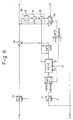
- FIG. 6 shows a cross-polarization interference canceller according to another embodiment of the present invention.
- the compensator of Fig. 6 comprises a interpolation calculation circuit 30 for generating a more precise error signal in the second half of the data intervals.
- the interpolation circuit 30 consists of a delay element 32, an adder 34, and an adder 36.
- the delay element 32 delays the output signal of the adder 18 by time T.
- the adder 34 adds a signal delayed by the delay element 32 to the output signal of the adder 18, and divides the sum by two by shifting the sum one bit position to the right.
- the output signal of the adder 34 corresponds to a mean value of two adjacent symbols.
- the adder 36 adds an output signal of the compensation signal generator 14 to the output signal of the adder 34, to calculate a more precise error signal in the second half of the data intervals.
- a selector 38 selects the output signal of the adder 18 in the first half of the data intervals and selects the output signal of the interpolation calculation circuit 30 in the second half of the data intervals and feeds the selected error signal to the compensation signal generator 14.
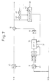
- Figure 7 shows a cross-polarization interference canceller according to another embodiment of the present invention.
- the canceller of Fig. 7 comprises a plurality of delay elements 40 each having a delay time of T and a calculator 42.
- a plurality of time adjacent data obtained by the delay elements 40 are input to the calculator 42.
- the calculator 42 calculates a more precise error signal ⁇ from the plurality of time adjacent data in the frequency 2 f .
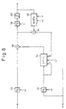
- Figure 8 is a block diagram showing the construction of a cross-polarization interference canceller according to another embodiment of the present invention.
- an analog/digital converter 50 for the main signal, an analog/digital converter 52 for the compensation signal, and a compensation signal generator 54 operate in synchronizm with a clock signal having a frequency of n f where n is an integer more than two and f is a frequency of the transmission data.
- the compensation signal generator 54 comprises an adaptive transversal filter having a construction similar to that of Fig. 4, except that delay time of the delay units is T/n.
- a compensation signal generated in the generator 54 is added to the main digital signal in an adder 56.
- An output signal of the adder 56 is a compensated baseband signal varying in frequency n f .
- the compensated baseband signal is sampled in synchronism with a clock signal having a frequency f in a frequency converter 58, and the sampled signal is fed to a decision circuit 60 used to determine the transmission data.
- the decision circuit 60 may be realized by merely extracting more significant data bits as described previously with reference to Fig. 1.
- a waveform generator 62 generates digital values of the baseband signal in frequency n f using the transmission data decided in the decision circuit 60 and coefficients of an impulse response of a transmission path.
- a subtracter 64 an exact error signal ⁇ is obtained in frequency n f by subtracting the compensated baseband signal from the estimate of the baseband signal output from the waveform generator 62.
- the waveform generator 62 of Fig. 8 is realized by a construction shown in Figure 9.
- four delay elements 66 constitute a tapped delay line retaining the values A -2 to A 2 .
- the values A -2 to A 2 are multiplied by the coefficients h -2 to h 2 , respectively, in multipliers 70 and are summed up in an adder 72.
- the memory 74 stores n sets of coefficients h -2 to h 2 and cyclically outputs the coefficients h -2 to h 2 , according to the value k output from the counter 73.
- the multipliers 70, the adder 72, and calculators 76, 78 can be replaced by a read-only memory 80 as shown in Figure 12.
- the values A 0 , A 1 and k are input to the read-only memory 80 as an address input, and the read-only memory 80 outputs the value V of the baseband signal determined by the address input.
- the values V are calculated in advance according to the formulae (2), (3) and (4) and are stored in the read-only memory 80.
Landscapes
- Engineering & Computer Science (AREA)
- Computer Networks & Wireless Communication (AREA)
- Signal Processing (AREA)
- Cable Transmission Systems, Equalization Of Radio And Reduction Of Echo (AREA)
Description
- The present invention relates to a cross-polarization interference canceller (XPIC) using a fractionally-spaced adaptive filter for generating a compensation signal.
- In a radio transmission, a technique utilizing orthogonal polarization, wherein signals are carried on both of the polarized waves orthogonal to each other (a vertically polarized wave (V) and a horizontally polarized wave (H)) in the same frequencies, has been realized in order to elevate the utilization efficiency of frequencies.
- In a system utilizing the orthogonal polarization, a high level of XPD (cross-polarization discrimination) is required to ensure stable transmission. Since the XPD sometimes deteriorates, for example, because of multipath fading in a microwave band or because of the presence of inclined raindrops in a frequency band higher than a semi-millimeter wave, the XPIC is introduced into the system in order to compensate for the deterioration of the XPD.
- An adaptive transversal filter is normally used for shaping a received signal in the other polarization wave to thereby generate a compensation signal. The compensation signal is added to a main signal to compensate for the cross-polarization interference distortion. Coefficients of the adaptive transversal filter are controlled by correlating signals at tapped delay line nodes of the filter with an error signal in a compensated signal.
- When a randomly varying phase difference occurs between two orthogonal polarization waves because of multipath feding, etc., the compensation signal generator operating in a frequency of transmission data cannot precisely compensate for the cross-polarization interference distortion. To overcome this problem, the introduction of a fractionally-spaced adaptive transversal filter having a fractionally-spaced tapped delay line and for updating the coefficients in a frequency more than two times the transmission data frequency, has been considered.
- EP-A-0 410 474 discloses a prior art cross-polarization canceller using a fractionally-spaced adaptive filter.
- In a conventional compensation signal generator using the fractionally-spaced adaptive transversal filter, the signals at tapped delay line nodes used to calculate the coefficients are updated in the operating frequency of the filter, but the error signal is updated only in the transmission data frequency, because estimates of transmission data used to generate the error signal are obtained only in the transmission data frequency in a decision-directed adaptation. Therefore, in the conventional compensation signal generator, the adaptive filter applies an error value in the first half of a data interval to an error value in the second half of the data interval.
- For this reason, the above compensation signal generator does not generate a precise compensation signal, particularly, in the second portions of data intervals. For example, in the extreme case of D/U = ∞, i.e., in the case that cross-polarization interference does not occur, although the compensation signal generator must generate a compensation signal having a level of zero, the compensation signal output from the generator has a level of zero in the first half of the data intervals and has levels freely varying in the second half of the data intervals, because the compensated signal in the second half of the data intervals are not reflected in the correction of levels of the compensation signal. This phenomenum wherein levels of zero and levels freely varying alternately appear is referred to as the "skewer" phenomenum.
- It is an object of the present invention to provide a fractionally-spaced cross-polarization interference canceller wherein the skewer phenomenum does not occur.
- It is another object of the present invention to provide a fractionally-spaced cross-polarization interference canceller wherein a more precise compensation is attained.
- In accordance with the present invention, there is provided a cross-polarization interference canceller for compensating for the effect of cross-polarization interference on transmission data carried on a first polarized wave, comprising:
- a first analog/digital conversion means for converting a first analog baseband signal obtained from the first polarized wave into a first digital signal;
- a second analog/digital conversion means for converting a second analog baseband signal obtained from a second polarized wave orthogonal to the first polarized wave into a second digital signal in an integral multiple frequency of a frequency of the transmission data;
- a filter means for shaping the second digital signal into a compensation signal in the integral multiple frequency; the filter means having coefficients controlled using an error signal in a compensated signal;
- an addition means for adding the compensation signal to the first digital signal to thereby output the compensated signal; and
- an error signal creating means for creating the error signal in the integral multiple frequency.
-
- Figure 1 is a block diagram showing the construction of a conventional fractionally-spaced cross-polarization interference canceller;
- Figure 2 is a diagram representing the "skewer" phenomenum;
- Figure 3 is a block diagram showing the construction of the fractionally-spaced cross-polarization interference canceller according to an embodiment of the present invention;
- Figure 4 is a block diagram showing a detailed construction of the
compensation signal generator 14 of Fig. 3; - Figure 5 is a block diagram showing the construction of the compensator according to another embodiment of the present invention;
- Figure 6 is a block diagram showing the construction of the canceller according to another embodiment of the present invention;
- Figure 7 is a block diagram showing the construction of the canceller according to another embodiment of the present invention;
- Figure 8 is a block diagram showing the construction of the canceller according to another embodiment of the present invention;
- Figure 9 is a block diagram showing the construction of an example of the
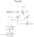
waveform generator 62 of Fig. 8; - Figure 10 is a block diagram showing the construction of another example of the
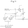
waveform generator 62 of Fig. 8; - Figure 11 is a block diagram showing the construction of another example of the
waveform generator 62 of Fig. 8; and - Figure 12 is a block diagram showing the construction of another example of the
waveform generator 62 of Fig. 8. - Before describing the preferred embodiments according to the present invention, examples of the related art are given with reference to the accompanying drawings.
- Figure 1 shows the aforementioned conventional fractionally-spaced cross-polarization interference canceller.
- A baseband signal obtained from a received vertically polarized wave (V) is converted into a digital signal consisting of a plurality of data bits in an analog/
digital converter 10. The analog/digital converter 10 samples an input signal in synchronizm with a clock signal having a frequency f that is transmission data frequency. A part of a baseband signal obtained from a received horizontally polarized wave (H) is distributed to generate a compensation signal. The distribution signal is converted into a digital signal consisting of a plurality of data bits in an analog/digital converter 12, and is fed into acompensation signal generator 14 including a transversal-type filter. The analog/digital converter 12 and thecompensation signal generator 14 operates in synchronizm with a clock signal having afrequency 2f. An output signal of thecompensation signal generator 14 is sampled in synchronizm with the transmission data clock f to convert the frequency from 2f into f in afrequency converter 16. A compensation signal output from thefrequency converter 16 is added to a main signal output from the analog/digital converter 10 in anadder 18. - Among data bits of the compensated signal output from the
adder 18, a prescribed number of more significant bits represent transmission symbols and the other less significant bits represent a decision error. Thus, the most significant bit among the other less significant bits corresponds to a sign of the decision error, and therefore, is used as an error signal ε for calculating coefficients of the transversal filter of thecompensation signal generator 14. - For example, in the case of 16 QAM (Quadrature Amplitude Modulation), a received signal is demodulated into an I-phase signal and a Q-phase signal, each having four levels. Therefore, more significant two bits represent transmission symbols and the third significant bit is used as the error signal. In Fig. 1 and the drawings described hereinafter, one of the circuits for an I-phase signal and a Q-phase signal is shown and the other is left out.
- As mentioned previously, in the conventional fractionally-spaced cross-polarization interference canceller shown in Fig. 1, a so-called "skewer" phenomenum occurs as shown in Figure 2, wherein levels of the compensation signal in the second half of the data intervals T varies freely, because the compensation signal in the second half of the data intervals T are discarded in the
frequency converter 16 and are not reflected in the correction of the compensation signal. - The preferred embodiments of the present invention will now be described with reference to the accompanying drawings.
- Figure 3 is a block diagram showing the construction of a cross-polarization interference canceller according to an embodiment of the present invention.
- In this embodiment, the
frequency converter 16 is provided in an output side of theadder 18, and the addition operation in theadder 18 is carried out infrequency 2f. The error signal ε is taken from a signal between theadder 18 and thefrequency converter 16. Therefore, the error signal ε is updated infrequency 2f. Since the compensation results in the second half of the data intervals as well as the first half are fed back to thecompensation signal generator 14, a compensation signal output from thecompensation signal generator 14 converges to a level of zero in the extreme case of D/U = ∞ and the "skewer" phenomenum does not occur. - The frequency converter 16 samples the output signal of the
adder 18 at the first half of the data intervals, to thus outputs a more precise compensation result in frequency f. - Figure 4 shows an example of a more detailed construction of the
compensation signal generator 14. Thecompensation signal generator 14 shown in Fig. 4 comprises a transversal-type filter consisting of sixdelay units 20, sevenmultipliers 22, and anadder 24. The sixdelay units 20 constitute a delay line having seven nodes spaced at T/2 intervals where T is a period of the transmission data. Input signals at the seven nodes are multiplied by coefficients C-3/2, C-1, C-1/2, C0, C1/2, C1, and C3/2, respectively, in themultipliers 22, and are summed up in theadder 24 to generate the compensation signal. The coefficients C-3/2 to C3/2 are controlled in acoefficient control unit 26. The most significant bits of input data at the seven delay line nodes D-3/2, D-1, D-1/2, D0, D1/2, D1, and D3/2, and the error bit ε are input to thecoefficient control unit 26. The coefficients C-3/2 to C3/2 are calculated according to MZF (Modified Zero-Forcing) algorithm represented by the following formula.
- Other known control algorithms such as LMS (Least Mean Square) and MSE (Mean Square Error) may be used in the
coefficient control unit 26. - Figure 5 is a block diagram of a cross-polarization interference canceller according to another embodiment of the present invention. In contrast to that of Fig. 1, an
adder 28 is further included. Theadder 28 adds the compensation signal to the main signal to generate the error signal infrequency 2f. Similar to the embodiment of Fig. 3, in the cross-polarization interference compensator of Fig. 5, the skewer phenomenum does not occur and a more precise compensation is attained. - Figure 6 shows a cross-polarization interference canceller according to another embodiment of the present invention. The compensator of Fig. 6 comprises a
interpolation calculation circuit 30 for generating a more precise error signal in the second half of the data intervals. Theinterpolation circuit 30 consists of adelay element 32, anadder 34, and anadder 36. Thedelay element 32 delays the output signal of theadder 18 by time T. Theadder 34 adds a signal delayed by thedelay element 32 to the output signal of theadder 18, and divides the sum by two by shifting the sum one bit position to the right. The output signal of theadder 34 corresponds to a mean value of two adjacent symbols. Theadder 36 adds an output signal of thecompensation signal generator 14 to the output signal of theadder 34, to calculate a more precise error signal in the second half of the data intervals. Aselector 38 selects the output signal of theadder 18 in the first half of the data intervals and selects the output signal of theinterpolation calculation circuit 30 in the second half of the data intervals and feeds the selected error signal to thecompensation signal generator 14. - Figure 7 shows a cross-polarization interference canceller according to another embodiment of the present invention. The canceller of Fig. 7 comprises a plurality of
delay elements 40 each having a delay time of T and acalculator 42. A plurality of time adjacent data obtained by thedelay elements 40 are input to thecalculator 42. Thecalculator 42 calculates a more precise error signal ε from the plurality of time adjacent data in thefrequency 2f. - Figure 8 is a block diagram showing the construction of a cross-polarization interference canceller according to another embodiment of the present invention.
- In Fig. 8, an analog/
digital converter 50 for the main signal, an analog/digital converter 52 for the compensation signal, and acompensation signal generator 54 operate in synchronizm with a clock signal having a frequency of nf where n is an integer more than two and f is a frequency of the transmission data. Thecompensation signal generator 54 comprises an adaptive transversal filter having a construction similar to that of Fig. 4, except that delay time of the delay units is T/n. A compensation signal generated in thegenerator 54 is added to the main digital signal in anadder 56. An output signal of theadder 56 is a compensated baseband signal varying in frequency nf. The compensated baseband signal is sampled in synchronism with a clock signal having a frequency f in afrequency converter 58, and the sampled signal is fed to adecision circuit 60 used to determine the transmission data. Thedecision circuit 60 may be realized by merely extracting more significant data bits as described previously with reference to Fig. 1. - A
waveform generator 62, described in detail later, generates digital values of the baseband signal in frequency nf using the transmission data decided in thedecision circuit 60 and coefficients of an impulse response of a transmission path. In asubtracter 64, an exact error signal ε is obtained in frequency nf by subtracting the compensated baseband signal from the estimate of the baseband signal output from thewaveform generator 62. - Since the value V of the baseband signal at any time can be represented by the formula

waveform generator 62 of Fig. 8 is realized by a construction shown in Figure 9. In Fig. 9, fourdelay elements 66 constitute a tapped delay line retaining the values A-2 to A2. Namely, the summation in formula (2) is calculated within a range from m = -2 to m = 2. The values A-2 to A2 are multiplied by the coefficients h-2 to h2, respectively, inmultipliers 70 and are summed up in anadder 72. A counter 73 counts the clock nf and cyclically outputs a count value k where k = 0, 1...n-1. Thememory 74 stores n sets of coefficients h-2 to h2 and cyclically outputs the coefficients h-2 to h2, according to the value k output from thecounter 73. At the timing of clock f, i.e., when k = 0, thememory 74 outputs h0 = 1 and h±1, ±2 = 0 . At the time displaced from the timing of clock f, i.e., when k = 1, 2, ...n-1, thememory 74 outputs hm = h(
- When the number of taps is two, the circuit is simplified as shown in Figure 10.
- Furthermore, upon considering an approximation of the baseband signal by linear interpolaration, the coefficients h0 and h1 are written as


memory 74 is replaced bycalculators - Furthermore, the
multipliers 70, theadder 72, andcalculators only memory 80 as shown in Figure 12. In Fig. 12, the values A0, A1 and k are input to the read-only memory 80 as an address input, and the read-only memory 80 outputs the value V of the baseband signal determined by the address input. The values V are calculated in advance according to the formulae (2), (3) and (4) and are stored in the read-only memory 80. - Reference signs in the claims are intended for better understanding and shall not limit the scope.
Claims (11)
- A cross-polarization interference canceller for compensating for the effect of cross-polarization interference on transmission data carried on a first polarized wave, comprising:a first analog/digital conversion means (10; 50) for converting a first analog baseband signal obtained from the first polarized wave into a first digital signal;a second analog/digital (12, 52) conversion means for converting a second analog baseband signal obtained from a second polarized wave orthogonal to the first polarized wave into a second digital signal in an integral multiple frequency of a frequency of the transmission data;a filter means (14; 54) for shaping the second digital signal into a compensation signal in the integral multiple frequency; the filter means having coefficients controlled using an error signal in a compensated signal;an addition means (18; 28; 56) for adding the compensation signal to the first digital signal to thereby output the compensated signal; andan error signal creating means for creating said an error signal in the integral multiple frequency.
- A cross-polarization interference canceller as claimed in claim 1, wherein the first analog/digital conversion means (10) performs the conversion in the transmission data frequency.
- A cross-polarization interference canceller, as claimed in claim 2, wherein the error signal creating means creates the error signal from the compensated signal output from the addition means and varies in the integral multiple frequency.
- A cross-polarization interference canceller, as claimed in claim 2, wherein the error signal creating means includesa unit (32, 34) for calculating a mean value of two adjacent transmission data,a unit (36) for adding the compensation signal output from the filter means to the mean value, anda unit (38) for selecting an output signal of the adding unit or the compensated signal output from the addition means in the integral multiple frequency as a signal used to create the error signal.
- A cross-polarization interference canceller, as claimed in claim 2, wherein the error signal creating means includesa delay line (40) having a plurality of taps spaced at intervals of transmission data to which the compensated signal is input, anda calculator (42) for creating the error signal from the values at the taps of the delay line in the integral multiple frequency.
- A cross-polarization interference canceller, as claimed in claim 1, wherein the first analog/digital conversion means (50) performs the conversion in the integral multiple frequency, and wherein the error signal creating means includesdecision means (58, 60) for deciding the transmission data from the compensated signal output from the addition means, to thereby output an estimate of the transmission data,estimate generating means (62) for generating an estimate of the baseband signal based on estimates of the transmission data determined in the decision means in the integral multiple frequency, andsubtraction means (64) for subtracting the compensated signal from the estimate of the baseband signal to thereby create the error signal in the integral multiple frequency.
- A cross-polarization interference canceller, as claimed in claim 6, wherein the estimate generating means includea delay line (66) having a plurality of taps spaced apart by intervals of the transmission data for concurrently providing a plurality of adjacent estimates of the transmission data output from the decision means,a counter (73) for counting a clock signal having the integral multiple frequency to thereby output a count, andan estimate determining means for determining the estimate of the baseband signal based on the estimates of the transmission data provided by the delay line and the said count.
- A cross-polarization interference canceller, as claimed in claim 7, wherein the estimate determining means includesa plurality of multipliers (70) for multiplying the estimates of the transmission data provided by the delay line by a set of coefficients, respectively,an adder (72) for summing up the multiplied estimates to thereby output the estimate of the baseband signal, anda coefficient providing means for providing the set of the coefficients according to the count.
- A cross-polarization interference canceller, as claimed in claim 8, wherein the coefficient providing means include
a memory (74) storing a plurality of sets of coefficients and outputting a set of the coefficients selected according to the count as an address input. - A cross-polarization interference canceller, as claimed in claim 8, wherein the coefficient providing means includes
a calculator (76, 78) for calculating the set of coefficients from the count. - A cross-polarization interference canceller, as claimed in claim 7, wherein the estimate determining means includes
a memory (80) storing a plurality of values of the estimate of the baseband signal and outputting a value of the estimate of the baseband signal selected according to the estimates of the transmission data provided by the delay line and the said count as an address input.
Applications Claiming Priority (6)
| Application Number | Priority Date | Filing Date | Title |
|---|---|---|---|
| JP194803/91 | 1991-07-08 | ||
| JP3194803A JP2711032B2 (en) | 1991-07-08 | 1991-07-08 | Fractional cross-polarization interference compensation method |
| JP3211520A JP2711033B2 (en) | 1991-07-29 | 1991-07-29 | Fractional cross-polarization interference compensator |
| JP211520/91 | 1991-07-29 | ||
| JP249206/91 | 1991-09-27 | ||
| JP3249206A JP2956724B2 (en) | 1991-09-27 | 1991-09-27 | Oversampling transversal equalizer |
Publications (3)
| Publication Number | Publication Date |
|---|---|
| EP0522534A2 EP0522534A2 (en) | 1993-01-13 |
| EP0522534A3 EP0522534A3 (en) | 1993-07-14 |
| EP0522534B1 true EP0522534B1 (en) | 1997-10-29 |
Family
ID=27326993
Family Applications (1)
| Application Number | Title | Priority Date | Filing Date |
|---|---|---|---|
| EP92111587A Expired - Lifetime EP0522534B1 (en) | 1991-07-08 | 1992-07-08 | Fractionally spaced crosspolarization interference canceller |
Country Status (4)
| Country | Link |
|---|---|
| US (1) | US5406589A (en) |
| EP (1) | EP0522534B1 (en) |
| CA (1) | CA2073082C (en) |
| DE (1) | DE69222895T2 (en) |
Cited By (1)
| Publication number | Priority date | Publication date | Assignee | Title |
|---|---|---|---|---|
| WO2011083077A2 (en) | 2010-01-07 | 2011-07-14 | Broadband United Gmbh | Device and method for compensating for and identifying crosstalk |
Families Citing this family (18)
| Publication number | Priority date | Publication date | Assignee | Title |
|---|---|---|---|---|
| US5838740A (en) * | 1996-04-17 | 1998-11-17 | Motorola, Inc. | Crosspole interference canceling receiver for signals with unrelated baud rates |
| IL154552A0 (en) * | 2000-08-31 | 2003-09-17 | Millimetrix Broadband Networks | Improved spatial efficiency for wireless rings and network of links in millimeter wave (mmw) communication systems |
| AU2001284377A1 (en) * | 2000-08-31 | 2002-03-13 | Millimetrix Broadband Networks Ltd. | Improved spatial spectral efficiency for wireless rings and network of links in millimeter wave (mmw) communication systems |
| US7046753B2 (en) * | 2004-06-29 | 2006-05-16 | Provigent Ltd. | Interference canceller with fast phase adaptation |
| JPWO2007043124A1 (en) * | 2005-09-30 | 2009-04-16 | 富士通マイクロエレクトロニクス株式会社 | Oversampling transversal equalizer |
| US7613260B2 (en) * | 2005-11-21 | 2009-11-03 | Provigent Ltd | Modem control using cross-polarization interference estimation |
| US7796708B2 (en) * | 2006-03-29 | 2010-09-14 | Provigent Ltd. | Adaptive receiver loops with weighted decision-directed error |
| US7643512B2 (en) | 2006-06-29 | 2010-01-05 | Provigent Ltd. | Cascaded links with adaptive coding and modulation |
| US7839952B2 (en) * | 2006-12-05 | 2010-11-23 | Provigent Ltd | Data rate coordination in protected variable-rate links |
| US7720136B2 (en) | 2006-12-26 | 2010-05-18 | Provigent Ltd | Adaptive coding and modulation based on link performance prediction |
| US8315574B2 (en) * | 2007-04-13 | 2012-11-20 | Broadcom Corporation | Management of variable-rate communication links |
| US7821938B2 (en) * | 2007-04-20 | 2010-10-26 | Provigent Ltd. | Adaptive coding and modulation for synchronous connections |
| US8001445B2 (en) * | 2007-08-13 | 2011-08-16 | Provigent Ltd. | Protected communication link with improved protection indication |
| US8040985B2 (en) | 2007-10-09 | 2011-10-18 | Provigent Ltd | Decoding of forward error correction codes in the presence of phase noise |
| EP2112772B1 (en) * | 2008-04-24 | 2016-08-31 | Alcatel Lucent | Method for reducing interference in a radio network equipment and equipment performing the method |
| GB2474180A (en) * | 2008-07-25 | 2011-04-06 | Smith International | PDC bit having split blades |
| US8615055B2 (en) * | 2009-03-30 | 2013-12-24 | Telefonaktiebolaget L M Ericsson (Publ) | Communication between modems in XPIC configuration for wireless applications |
| US20110147350A1 (en) * | 2010-12-03 | 2011-06-23 | Uvtech Systems Inc. | Modular apparatus for wafer edge processing |
Family Cites Families (10)
| Publication number | Priority date | Publication date | Assignee | Title |
|---|---|---|---|---|
| NL7902053A (en) * | 1979-03-15 | 1980-09-17 | Philips Nv | ECHO COMPENSATOR FOR HOMOCHRONOUS DATA TRANSMISSION SYSTEMS. |
| US4550415A (en) * | 1983-11-16 | 1985-10-29 | At&T Bell Laboratories | Fractionally spaced equalization using nyquist-rate coefficient updating |
| NL190886C (en) * | 1986-05-19 | 1994-10-03 | Nippon Telegraph & Telephone | Digital signal demodulation system. |
| JPS6477235A (en) * | 1987-09-18 | 1989-03-23 | Fujitsu Ltd | Compensating device for interference between cross-polarized waves |
| JPH01235405A (en) * | 1988-03-16 | 1989-09-20 | Toshiba Corp | Automatic equalizer |
| JP2653371B2 (en) * | 1989-02-20 | 1997-09-17 | 富士通株式会社 | Adaptive equalizer |
| CA2022050C (en) * | 1989-07-27 | 1993-03-23 | Toru Matsuura | Cross-polarization interference cancellation system capable of stably carrying out operation |
| US5249289A (en) * | 1989-09-28 | 1993-09-28 | International Business Machines Corporation | System and method for rebuilding edited digital audio files |
| JP2536207B2 (en) * | 1990-01-23 | 1996-09-18 | 日本電気株式会社 | Interference compensator |
| JP3169646B2 (en) * | 1991-09-25 | 2001-05-28 | 日本電気株式会社 | Cross polarization interference compensator |
-
1992
- 1992-07-03 CA CA002073082A patent/CA2073082C/en not_active Expired - Fee Related
- 1992-07-07 US US07/909,712 patent/US5406589A/en not_active Expired - Lifetime
- 1992-07-08 DE DE69222895T patent/DE69222895T2/en not_active Expired - Lifetime
- 1992-07-08 EP EP92111587A patent/EP0522534B1/en not_active Expired - Lifetime
Cited By (3)
| Publication number | Priority date | Publication date | Assignee | Title |
|---|---|---|---|---|
| WO2011083077A2 (en) | 2010-01-07 | 2011-07-14 | Broadband United Gmbh | Device and method for compensating for and identifying crosstalk |
| DE102010004178A1 (en) | 2010-01-07 | 2011-07-14 | Broadband United GmbH, 93047 | Apparatus and method for compensation and identification of crosstalk |
| US9001880B2 (en) | 2010-01-07 | 2015-04-07 | Broadband United Gmbh | Device and method for identification and cancellation of crosstalk |
Also Published As
| Publication number | Publication date |
|---|---|
| DE69222895D1 (en) | 1997-12-04 |
| CA2073082A1 (en) | 1993-01-09 |
| EP0522534A2 (en) | 1993-01-13 |
| CA2073082C (en) | 1997-09-09 |
| EP0522534A3 (en) | 1993-07-14 |
| US5406589A (en) | 1995-04-11 |
| DE69222895T2 (en) | 1998-03-19 |
Similar Documents
| Publication | Publication Date | Title |
|---|---|---|
| US5406589A (en) | Fractionally spaced cross-polarization interference canceller | |
| CA1221749A (en) | Fractionally spaced equalization using nyquist-rate coefficient updating | |
| EP0443333B1 (en) | Cross-polarization interference canceller | |
| JP3375139B2 (en) | Adaptive array transceiver | |
| KR100355326B1 (en) | Ofdm communication apparatus and method for estimating of transmission path | |
| EP0426026B1 (en) | Equalizer | |
| US8254509B2 (en) | Receiver | |
| US5175747A (en) | Equalizer | |
| EP0567211B1 (en) | Adaptive receiver for multipath fading channels | |
| EP0410474B1 (en) | Cross-polarization interference cancellation system capable of stably carrying out operation | |
| EP0216183A2 (en) | Decision feedback equalizer with a pattern detector | |
| EP1249979A2 (en) | Front end processor and method of compensating nonlinear distortion | |
| US5228058A (en) | Adaptive equalizer | |
| US5970094A (en) | Adaptive equalizer employing filter input circuit in a circular structure | |
| US5359628A (en) | Channel impulse response estimator for use in an adaptive maximum likelihood sequence estimation receiver which is applicable to a communication system having a channel characteristic with rapid fluctuation | |
| EP0534384B1 (en) | Cross-polarization interference canceller | |
| EP0725488A2 (en) | Data receiving system for receiving data signal faded and delayed | |
| US5905717A (en) | Echo canceller for a packet signal | |
| JP3180240B2 (en) | Adaptive equalizer | |
| US20100208787A1 (en) | Waveform equalizer and method for controlling the same, as well as receiving apparatus and method for controlling the same | |
| JP2711032B2 (en) | Fractional cross-polarization interference compensation method | |
| JP3138586B2 (en) | Adaptive equalizer and adaptive diversity equalizer | |
| JP2932380B1 (en) | Interference wave detection circuit | |
| JPS59139717A (en) | automatic equalizer | |
| JPH0738470A (en) | Adaptive equalizer |
Legal Events
| Date | Code | Title | Description |
|---|---|---|---|
| PUAI | Public reference made under article 153(3) epc to a published international application that has entered the european phase |
Free format text: ORIGINAL CODE: 0009012 |
|
| AK | Designated contracting states |
Kind code of ref document: A2 Designated state(s): DE FR GB |
|
| PUAL | Search report despatched |
Free format text: ORIGINAL CODE: 0009013 |
|
| AK | Designated contracting states |
Kind code of ref document: A3 Designated state(s): DE FR GB |
|
| 17P | Request for examination filed |
Effective date: 19930720 |
|
| GRAG | Despatch of communication of intention to grant |
Free format text: ORIGINAL CODE: EPIDOS AGRA |
|
| 17Q | First examination report despatched |
Effective date: 19960910 |
|
| GRAH | Despatch of communication of intention to grant a patent |
Free format text: ORIGINAL CODE: EPIDOS IGRA |
|
| GRAH | Despatch of communication of intention to grant a patent |
Free format text: ORIGINAL CODE: EPIDOS IGRA |
|
| GRAA | (expected) grant |
Free format text: ORIGINAL CODE: 0009210 |
|
| AK | Designated contracting states |
Kind code of ref document: B1 Designated state(s): DE FR GB |
|
| PG25 | Lapsed in a contracting state [announced via postgrant information from national office to epo] |
Ref country code: FR Free format text: LAPSE BECAUSE OF FAILURE TO SUBMIT A TRANSLATION OF THE DESCRIPTION OR TO PAY THE FEE WITHIN THE PRESCRIBED TIME-LIMIT Effective date: 19971029 |
|
| REF | Corresponds to: |
Ref document number: 69222895 Country of ref document: DE Date of ref document: 19971204 |
|
| EN | Fr: translation not filed | ||
| PLBE | No opposition filed within time limit |
Free format text: ORIGINAL CODE: 0009261 |
|
| STAA | Information on the status of an ep patent application or granted ep patent |
Free format text: STATUS: NO OPPOSITION FILED WITHIN TIME LIMIT |
|
| 26N | No opposition filed | ||
| REG | Reference to a national code |
Ref country code: GB Ref legal event code: IF02 |
|
| PGFP | Annual fee paid to national office [announced via postgrant information from national office to epo] |
Ref country code: GB Payment date: 20110706 Year of fee payment: 20 Ref country code: DE Payment date: 20110706 Year of fee payment: 20 |
|
| REG | Reference to a national code |
Ref country code: DE Ref legal event code: R071 Ref document number: 69222895 Country of ref document: DE |
|
| REG | Reference to a national code |
Ref country code: DE Ref legal event code: R071 Ref document number: 69222895 Country of ref document: DE |
|
| REG | Reference to a national code |
Ref country code: GB Ref legal event code: PE20 Expiry date: 20120707 |
|
| PG25 | Lapsed in a contracting state [announced via postgrant information from national office to epo] |
Ref country code: GB Free format text: LAPSE BECAUSE OF EXPIRATION OF PROTECTION Effective date: 20120707 Ref country code: DE Free format text: LAPSE BECAUSE OF EXPIRATION OF PROTECTION Effective date: 20120710 |