EP0516098B1 - High accuracy beam blanker - Google Patents
High accuracy beam blanker Download PDFInfo
- Publication number
- EP0516098B1 EP0516098B1 EP92108974A EP92108974A EP0516098B1 EP 0516098 B1 EP0516098 B1 EP 0516098B1 EP 92108974 A EP92108974 A EP 92108974A EP 92108974 A EP92108974 A EP 92108974A EP 0516098 B1 EP0516098 B1 EP 0516098B1
- Authority
- EP
- European Patent Office
- Prior art keywords
- blanker
- plates
- voltage
- deflection
- pairs
- Prior art date
- Legal status (The legal status is an assumption and is not a legal conclusion. Google has not performed a legal analysis and makes no representation as to the accuracy of the status listed.)
- Expired - Lifetime
Links
Images




Classifications
-
- H—ELECTRICITY
- H01—ELECTRIC ELEMENTS
- H01J—ELECTRIC DISCHARGE TUBES OR DISCHARGE LAMPS
- H01J37/00—Discharge tubes with provision for introducing objects or material to be exposed to the discharge, e.g. for the purpose of examination or processing thereof
- H01J37/30—Electron-beam or ion-beam tubes for localised treatment of objects
- H01J37/304—Controlling tubes by information coming from the objects or from the beam, e.g. correction signals
-
- H—ELECTRICITY
- H01—ELECTRIC ELEMENTS
- H01J—ELECTRIC DISCHARGE TUBES OR DISCHARGE LAMPS
- H01J37/00—Discharge tubes with provision for introducing objects or material to be exposed to the discharge, e.g. for the purpose of examination or processing thereof
- H01J37/02—Details
- H01J37/04—Arrangements of electrodes and associated parts for generating or controlling the discharge, e.g. electron-optical arrangement or ion-optical arrangement
- H01J37/045—Beam blanking or chopping, i.e. arrangements for momentarily interrupting exposure to the discharge
Definitions
- This invention relates to a method of constructing a double deflection beam blanker according to the preamble of claim 1 and to a double deflection beam blanker according to the preamble of claim 5.
- the beam blanker is an integral component of electron optical columns dedicated to chip and mask lithography, circuit testing and inspection, and other applications where a charged particle beam must be rapidly turned off and on at a target plane (i.e., the surface of a substrate).
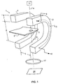
- a typical beam blanker 1 is shown in Figure 1.
- the applied blanker voltage is, in fact, time dependent, i.e. the voltage is varied during the transition between the beam "on” and “off” states. This variation in blanker voltage during the transition, coupled with the beam transit for those electrons passing through aperture 5 results in undesirable motion at the target 26.
- U.S. Patent 4,445,041 discloses a double deflection blanker (see Figure 1) in which the bottom halves 9 of plates 2 deflect the electrons which have passed through aperture 5. This second deflection of the electrons attempts to compensate for this time-dependent blanker voltage by creating a steady state voltage effect, thereby minimizing the beam jitter.
- an improved blanker includes a delay line length which is a function of a predetermined voltage.
- Optimal delay line length minimizes beam jitter and compensates for fringe-field effects.
- closed-form trajectory equations are derived in accordance with the present invention to provide an exact understanding of the operation and interaction of the blanker geometry, blanker voltage, and beam in order to provide the optimal delay line length. These equations describe the electron-optical mechanics of the beam-blanker interaction and provide the means to determine the optimum geometric parameters and hence performance for the blanker. Also, with these equations, voltage effects such as ringing, overshoot, and rise and fall time of the blanker can be precisely determined.
- the reduction in blanker-induced beam jitter is achieved by finding the optimum blanker voltage propagation delay between the upper to lower pair of plates. From this information, the physical length of the delay line is accurately determined for any beam voltage. Different delay line lengths, hence different blankers, are provided for specific blanker voltages in order to optimize blanker performance.
- equations determine the required mechanical tolerances for the blanker which aids in decreasing beam positional jitter. Furthermore, a method to measure the effect of electrostatic fringe-fields on blanker action is provided which includes construction of a model of the blanker.
- This model incorporates a delay line length, which minimizes beam jitter based on the assumption there is no fringe field effect.
- the model is installed in a working system and the fringe field effect is determined by measuring the effective length of the blanking plates.
- This effective length is derived from the measured blanker plate deflection sensitivity, i.e. the beam deflection angle per applied voltage. In general, this length is greater than the physical plate length.
- An equivalent statement is that the beam is typically deflected off-axis a greater distance at a known axial location below the blanker than expected from using the formula describing this quantity in terms of the physical length of the blanking plates.
- a new value for the optimum delay line length is then determined based on the measured "effective length" of the prototype blanker.
- a blanker identical in geometry to the prototype is constructed except having a different delay line length based on the effective length.
- a blanker incorporating these values is then constructed.
- two alignment apertures are placed above and below the blanker to define the maximum off-axis beam excursion (for a movable beam stop) or to specify the concentricity of the beam stop to the blanker axis (for a fixed beam stop).
- the size of these apertures is typically a function of the maximum allowable beam jitter specified.
- a range in blanker delay line length is determined from the equations, consistent with the permissible amount of beam jitter. This tolerance range corresponds to a maximum allowable off-axis variation from the ideal beam axis, which is then mechanically defined by the blanker alignment aperture diameter.
- this invention results in greater beam positional accuracy at the target substrate while blanking.
- Figure 1 illustrates a typical double-deflection beam blanker with delay line and beam stop both as used in the prior art and in accordance with the invention.
- Figure 2 shows a typical double-deflection blanker, lens, and substrate geometry in the prior art and also in accordance with the present invention.
- Figure 3 illustrates a beam diagram showing the general behavior as the lens excitation is varied about the blanker midgap.
- Figure 4 compares the performance of the prior art blanker with that of the present invention operating at 20 kV beam voltage.
- Figure 5 compares the beam jitter of the prior art blanker with that of the present invention operating at 10 kV beam voltage.
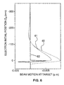
- Figure 6 illustrates blanker-induced beam motion X * (Z o ) sensitivity to various drift length Z D settings.
- Figure 7 compares blanker motion X * (Z o ) curves using blanker conditions noted in the prior art.
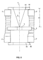
- Figure 8 shows an end view of a double-deflection blanker with alignment apertures.
- Figure 9 illustrates part of the process and geometries used in the present invention to determine the effective blanker plate length.
- Figure 10 shows a typical comparison of the plate length Lp and gap g to the effective plate length L ⁇ p and effective gap g ⁇ after fringe field effects have been determined.
- a steady state voltage, as noted previously, applied to a blanker produces a deflection of an electron beam.
- a conventional electron focusing lens 12 which is placed between blanker 1 and target 26 focuses the beam onto the target 26.
- the desired object point of focusing lens 12 is the beam cross-over or rocking point.
- the double-deflection blanker 1 has an apparent, in optics terminology "virtual”, rocking or pivot point in gap 8 between the upper and lower pairs of plates 2. If focusing lens 12 images this rocking point, the electron beam remains on-axis while applying a DC blanker voltage.
- Figure 2 illustrates typical blanker geometry for two beam trajectories.
- Curve 20 shows that when the beam emitted from beam source 11 is sufficiently deviated from beam axis 4, beam stop 6 stops the beam and effectively results in an "off" state. However, if beam stop 6 were not present, curve 21 shows that lens 12 would direct the beam 27 to hit target 28 on axis 4 given
- Curve 22 indicates a beam trajectory passing through the blanker during voltage decay which will result in beam jitter at the substrate 26.
- the apparent (virtual) beam off-axis deflection is shown by dashed line 23.
- Beam jitter X * is defined as a function of both the axial evaluation point Z e (or the lens object position) and the initial position Z o of the electron at the moment the blanker starts its off-to-on transition.
- X * (Z e ,Z o ) describes X* as a function of Z e , Z o .
- the rocking point of double-deflection blanker 1 lies at the midpoint of the gap 8 (see Figure 1) along beam axis 4.
- vector 31 corresponds to the magnitude 34 of the positional jitter at the lens image plane 26. If Z e > L p + g/2 , indicated by point 38 then vector 32 likewise corresponds to the beam shift 35 at the lens image plane 26.
- Beam jitter provides a measure of blanker performance in terms of movement (of the beam) per applied force (by the blanker) with dimensions of [time ⁇ distance].
- the distance unit is defined as the maximum positional offset during beam transmission.
- the time unit is defined as that interval during which the beam is still outside its specified positional accuracy range.
- the double-deflection beam blanker 1 (see Figure 1) and its operating characteristics are completely defined by two sets of blanker variables.
- the first set of variables includes the geometrical parameters of the blanker: the plate length L p (7), the plate separation D (3), the gap g (8) between upper and lower pairs of plates, the delay line length L D , and the blanker aperture diameter d ap of aperture 5.
- the plate length L p is made as large as possible to improve deflection sensitivity, i.e. deflection per applied voltage.
- An increase in plate length L p provides more opportunity for the electron beam to be acted upon, thereby increasing its deflection. This allows the blanker voltage to be reduced thereby increasing the speed of the blanker driver.
- this dimension is limited to a ratio L p /D as determined by the magnitude of the impedance desired to make double-deflection beam blanker 1 a transmission line electrically matched to the blanker driver electronics.
- An impedance mismatch results in reflections at the input 9 and output 10 of the delay line as the voltage signal propagates through plates 2.
- V(t)/V d exp(-at) ⁇ cos (bt)
- This equation models ringing, or oscillation in the voltage, overshoot, when the voltage is above the intended voltage, and the rise and fall time where V d is the maximum applied blanker voltage.
- This description of the blanker voltage is a general solution for any blanker driver circuit described as a resistive, inductive, capacitive (RLC) network.
- RLC resistive, inductive, capacitive
- the beam motion is apparent because X * (Z o ) is the off-axis beam position within the blanker, as magnified by the lens, but does not correspond to the actual trajectory within the blanker X(Z, Z o ) .
- the propagation delay of the blanker voltage through plates 2 can be physically defined in three ways.
- the first way is shown in Figure 1, where a U-shaped blanker plate structure conducts the blanking signal V d (t) from its input 9 at the upper pair of plates 2 to the exit point 10 at the lower set of plates 2 via the length L D .
- the horseshoe-shaped blanker can also be replaced by a wire or cable connecting two separate pairs of plates (not shown). In that case, the propagation velocity V cable is determined by the cable dielectric and the delay line length.
- T D L D /V cable
- the third case uses an amplifier stage to set the time delay between a blanking signal applied to the upper and lower pairs of plates (also not shown). This latter configuration is particularly useful in the case of blanking ions, which move slower than electrons at a given beam voltage and, therefore, require longer time delays in the blanker.
- Two scales, t0 and z0, are indicated on the horizontal axis of Figure 4.
- each solution in Table I as derived from, for example, equations 3c, 2c, 1b, etc., describes the amount of beam jitter in a particular segment.
- the size of each segment is determined by the blanker geometry (for example, z1, z2 and z3) and the delay line length L d .
- the real part of the complex variable equation is combined with the geometrical data on the blankers (already provided) to solve for the apparent beam jitter.
- Table I applies to the transition from beam “off” to “on”, while Table II applies to the transition from “on” to “off”.
- L D is determined by recognizing that L D is equal to T D multiplied by the blanker voltage propagation velocity c when the blanker voltage dielectric constant is one.
- a blanker voltage applied to the plates produces an electromagnetic field transverse to the electron beam axis.
- this field does not end at the finite end of the plate, but instead extends off the plate into space. This extension is called the fringe-field.
- the fringe-field effectively increases the length of the deflection field beyond that defined by the physical plate length. Without a measurement of this field and subsequent incorporation in the blanker design, the blanker positional accuracy is degraded.
- the present invention in one embodiment compensates for fringe-field effects by a three-step process.
- First as seen above, the equations of motion are used to predict the optimum delay line length.
- the beam is focused at center 94 of blanker aperture 5. Provision is made to collect the current at center 94 preamplify it, and send it to Z-input of a video system 90 where it results in intensity modulation of the video image.
- the x-y raster scan signal is simultaneously sent from the driver 91 to (a) the video system 90 and (b) a set of beam scan coils 92. In this manner an image of blanker aperture 5 is formed at the video 90.
- a first blanker aperture 5 image is recorded with a camera (not shown), which corresponds to both blanking plates 2 being at ground potential, so the beam is undeflected.
- a second image is recorded after having impressed a known DC blanker voltage on plates 2.
- the second image reveals a translational shift ⁇ X image in the position of center 94 as seen by distance 95 compared to the first image (undeflected beam case).
- the effective length L p ⁇ and gap g ⁇ are thus determined.
- the delay time is recalculated based on the measured effective plate length.
- a final model of the blanker is constructed for a particular, given voltage.
- FIG. 4 illustrates that a blanker in accordance with the present invention improves blanker performance when used at a 20 kV beam voltage because of the increased accuracy of the exact equations of motion and the incorporation of fringe fields.
- Curve 40 of Figure 4 shows the beam jitter induced by the prior art design at 20 kV which does not compensate for the blanker plate fringe fields.
- the maximum positional offset 41 is 0.03 ⁇ m .
- the beam is misplaced outside a 0.01 ⁇ m limit (i.e. the limit defines when the electron beam is within 0.01 ⁇ m from target) shown by dashed lines 42 for 1.4 nsec. This corresponds to 22% of the dose in the first pixel being misplaced in a raster-scan electron beam system, which blanks at 160 MHz.
- Curve 43 shows the blanker with an increased delay line length as determined by the method of the present disclosure which compensates for the fringe field effect. In this case, the beam positional accuracy is maintained at all times during the blanker exposure.
- Figure 5 shows that the 20 kV prior art design is unsuitable for 10 kV operation.
- the operating parameters noted in Figure 4 are used.
- the prior art blanker has a 0.50 ⁇ m maximum positional offset 51 as shown by curve 50.
- the time duration outside the 0.01 ⁇ m beam accuracy specification (see dashed line 52) is 3.3 nsec.
- the blanker in accordance with the present invention remains within the positional accuracy range for all times as shown by curve 53.
- Figure 7 shows another example of the inadequacy of the blanker operation as discussed in the Gesley and Condran publication.
- the solid curve 70 is that found using the solutions given in the present disclosure.
- the dashed curve 71 is taken from the '041 patent and is matched only at the origin, its scale is given by the dashed lines.
- the numerical analysis as disclosed in the Gesley and Condran 0 publication cannot determine the magnitude or duration of the "blip" region, which is the rapidly changing portion of the apparent beam jitter.
- a mechanical means is introduced to ensure the 5 off-axis beam position with respect to the blanker axis is within a specified limit (assuming the use of a moveable aperture as beam stop). This is accomplished by placing alignment plates 80, 82 having apertures 81, 83, seen in Figure 8, above and below respectively the blanker body 1 to define the blanker mechanical axis 4.
- the apertures 81, 83 define the maximum off-axis beam excursion. Limiting the beam offset ensures that maximum variation of the delay line length is kept to a specified minimum.
- apertures 81, 83 specify the concentricity of beam stop 6 to the blanker axis 4.
- alignment apertures 81 and 83 each have a diameter of 600 mm, and aperture 5 has a diameter of 50 mm.
- the diameter of alignment apertures 81, 83 is the maximum allowed in order to maintain positional accuracy of the beam within 0.01 ⁇ m of the target.
- the delay length L D has a tolerance which defines the outside limits of this positional accuracy. For this example, by using Tables I and II, L D is determined to be 209.5 mm with a tolerance of 0.3 mm.
Landscapes
- Chemical & Material Sciences (AREA)
- Analytical Chemistry (AREA)
- Electron Beam Exposure (AREA)
- Manufacture And Refinement Of Metals (AREA)
- Laser Beam Processing (AREA)
- Welding Or Cutting Using Electron Beams (AREA)
- Manufacture Of Electron Tubes, Discharge Lamp Vessels, Lead-In Wires, And The Like (AREA)
- Electron Sources, Ion Sources (AREA)
- Optical Elements Other Than Lenses (AREA)
Abstract
Description
- This invention relates to a method of constructing a double deflection beam blanker according to the preamble of
claim 1 and to a double deflection beam blanker according to the preamble ofclaim 5. - The beam blanker is an integral component of electron optical columns dedicated to chip and mask lithography, circuit testing and inspection, and other applications where a charged particle beam must be rapidly turned off and on at a target plane (i.e., the surface of a substrate). A
typical beam blanker 1 is shown in Figure 1. A steady state voltage applied tobeam blanker 1, comprising two identical vertically alignedU-shaped plates 2 spaced apart bydistance 3, produces an electromagnetic field transverse to abeam axis 4. This field deflects the electrons or ions (which comprise the beam emanating from beam source 11) off-axis away fromaperture 5 causing the electrons or ions to become embedded inbeam stop 6, thereby stopping any beam current from being transmitted pastbeam stop 6. - However, the applied blanker voltage is, in fact, time dependent, i.e. the voltage is varied during the transition between the beam "on" and "off" states. This variation in blanker voltage during the transition, coupled with the beam transit for those electrons passing through
aperture 5 results in undesirable motion at thetarget 26. - Various structures have been proposed to eliminate the problem of beam jitter. For example, U.S. Patent 4,445,041 (hereinafter the '041 reference) discloses a double deflection blanker (see Figure 1) in which the
bottom halves 9 ofplates 2 deflect the electrons which have passed throughaperture 5. This second deflection of the electrons attempts to compensate for this time-dependent blanker voltage by creating a steady state voltage effect, thereby minimizing the beam jitter. - However, this reference describes solely an operation of the beam blanker at a 20kV beam voltage. An extension of this prior art disclosure to other beam voltages results in serious degradation in performance. Therefore, a need arises for a beam blanker which operates within the positional accuracy range at all times, for all beam voltages.
- Thus, it is the object of the present invention to provide a method for constructing a double deflection beam blanker which has superior performance at any selected beam voltage.
- The fore-going object is solved with a method having the eatures as set out in
claim 1. - In accordance with the invention, an improved blanker includes a delay line length which is a function of a predetermined voltage. Optimal delay line length minimizes beam jitter and compensates for fringe-field effects. Specifically, closed-form trajectory equations are derived in accordance with the present invention to provide an exact understanding of the operation and interaction of the blanker geometry, blanker voltage, and beam in order to provide the optimal delay line length. These equations describe the electron-optical mechanics of the beam-blanker interaction and provide the means to determine the optimum geometric parameters and hence performance for the blanker. Also, with these equations, voltage effects such as ringing, overshoot, and rise and fall time of the blanker can be precisely determined.
- The reduction in blanker-induced beam jitter is achieved by finding the optimum blanker voltage propagation delay between the upper to lower pair of plates. From this information, the physical length of the delay line is accurately determined for any beam voltage. Different delay line lengths, hence different blankers, are provided for specific blanker voltages in order to optimize blanker performance.
- Additionally, these equations determine the required mechanical tolerances for the blanker which aids in decreasing beam positional jitter. Furthermore, a method to measure the effect of electrostatic fringe-fields on blanker action is provided which includes construction of a model of the blanker.
- This model incorporates a delay line length, which minimizes beam jitter based on the assumption there is no fringe field effect.
- The model is installed in a working system and the fringe field effect is determined by measuring the effective length of the blanking plates. This effective length is derived from the measured blanker plate deflection sensitivity, i.e. the beam deflection angle per applied voltage. In general, this length is greater than the physical plate length. An equivalent statement is that the beam is typically deflected off-axis a greater distance at a known axial location below the blanker than expected from using the formula describing this quantity in terms of the physical length of the blanking plates.
- A new value for the optimum delay line length is then determined based on the measured "effective length" of the prototype blanker.
- A blanker identical in geometry to the prototype is constructed except having a different delay line length based on the effective length. A blanker incorporating these values is then constructed.
- In one embodiment, two alignment apertures are placed above and below the blanker to define the maximum off-axis beam excursion (for a movable beam stop) or to specify the concentricity of the beam stop to the blanker axis (for a fixed beam stop). The size of these apertures is typically a function of the maximum allowable beam jitter specified. A range in blanker delay line length is determined from the equations, consistent with the permissible amount of beam jitter. This tolerance range corresponds to a maximum allowable off-axis variation from the ideal beam axis, which is then mechanically defined by the blanker alignment aperture diameter.
- Therefore, this invention results in greater beam positional accuracy at the target substrate while blanking.
- Figure 1 illustrates a typical double-deflection beam blanker with delay line and beam stop both as used in the prior art and in accordance with the invention.
- Figure 2 shows a typical double-deflection blanker, lens, and substrate geometry in the prior art and also in accordance with the present invention.
- Figure 3 illustrates a beam diagram showing the general behavior as the lens excitation is varied about the blanker midgap.
- Figure 4 compares the performance of the prior art blanker with that of the present invention operating at 20 kV beam voltage.
- Figure 5 compares the beam jitter of the prior art blanker with that of the present invention operating at 10 kV beam voltage.
- Figure 6 illustrates blanker-induced beam motion X*(Z o ) sensitivity to various drift length Z D settings.
- Figure 7 compares blanker motion X*(Z o ) curves using blanker conditions noted in the prior art.
- Figure 8 shows an end view of a double-deflection blanker with alignment apertures.
- Figure 9 illustrates part of the process and geometries used in the present invention to determine the effective blanker plate length.
- Figure 10 shows a typical comparison of the plate length Lp and gap g to the effective plate length


- A steady state voltage, as noted previously, applied to a blanker produces a deflection of an electron beam. As seen in Figure 1, a conventional
electron focusing lens 12 which is placed betweenblanker 1 andtarget 26 focuses the beam onto thetarget 26. The desired object point of focusinglens 12 is the beam cross-over or rocking point. The double-deflection blanker 1 has an apparent, in optics terminology "virtual", rocking or pivot point ingap 8 between the upper and lower pairs ofplates 2. If focusinglens 12 images this rocking point, the electron beam remains on-axis while applying a DC blanker voltage. - Figure 2 illustrates typical blanker geometry for two beam trajectories.
Curve 20 shows that when the beam emitted frombeam source 11 is sufficiently deviated frombeam axis 4,beam stop 6 stops the beam and effectively results in an "off" state. However, ifbeam stop 6 were not present,curve 21 shows thatlens 12 would direct thebeam 27 to hittarget 28 onaxis 4 given - (i) the blanker voltage was constant and
- (ii) the lens excitation focused the blanker rocking point, defined by the intersection of
dashed line 28 with thevertical beam axis 4, at thesubstrate 26. -
Curve 22 indicates a beam trajectory passing through the blanker during voltage decay which will result in beam jitter at thesubstrate 26. The apparent (virtual) beam off-axis deflection is shown by dashedline 23. Beam jitter X* is defined as a function of both the axial evaluation point Z e (or the lens object position) and the initial position Z o of the electron at the moment the blanker starts its off-to-on transition. Hence, X*(Z e ,Z o ) describes X* as a function of Z e , Z o . Themagnitude 25 of the positional jitter at thelens image plane 26 is given by
lens 12. - The rocking point of double-
deflection blanker 1 lies at the midpoint of the gap 8 (see Figure 1) alongbeam axis 4. Figure 3 illustrates that if
point 36, where L p is the plate length 7 and g is the width of gap 8 (both shown in Figure 1), thenlens 12 directs thebeam 30 to hittarget 28 anaxis 4. Hence, with this rocking point, there is no off-axis beam shift (see dotted line 33) when a steady state voltage is applied to the blanker. - However, if

point 37 thenvector 31, transverse tobeam axis 4 and pointing to theray 33 of the virtual trajectory, will increase the beam jitter magnitude and result in a beam shift during application of a DC blanker voltage.Vector 31 corresponds to themagnitude 34 of the positional jitter at thelens image plane 26. If Z e > L p + g/2, indicated by point 38 thenvector 32 likewise corresponds to thebeam shift 35 at thelens image plane 26. - However, even when Ze = L p + g/2, some beam jitter (time-dependent motion) is inevitable. The present invention minimizes this motion by proper setting of the delay line length LD.
- Beam jitter provides a measure of blanker performance in terms of movement (of the beam) per applied force (by the blanker) with dimensions of [time × distance]. The distance unit is defined as the maximum positional offset during beam transmission. The time unit is defined as that interval during which the beam is still outside its specified positional accuracy range.
- To reduce beam jitter for any double-deflection beam blanker, the operation and interaction of the
blanker 5 geometry, the blanker voltage, and the beam itself should be fully understood. One embodiment of the present invention, using the derived equations shown in Tables I and II below, provides a method for ensuring a high accuracy beam blanker. - The double-deflection beam blanker 1 (see Figure 1) and its operating characteristics are completely defined by two sets of blanker variables. The first set of variables includes the geometrical parameters of the blanker: the plate length L p (7), the plate separation D (3), the gap g (8) between upper and lower pairs of plates, the delay line length L D , and the blanker aperture diameter d ap of
aperture 5. - In general, the plate length L p is made as large as possible to improve deflection sensitivity, i.e. deflection per applied voltage. An increase in plate length L p provides more opportunity for the electron beam to be acted upon, thereby increasing its deflection. This allows the blanker voltage to be reduced thereby increasing the speed of the blanker driver. However, in high speed blanking circuits, this dimension is limited to a ratio L p /D as determined by the magnitude of the impedance desired to make double-deflection beam blanker 1 a transmission line electrically matched to the blanker driver electronics. An impedance mismatch results in reflections at the
input 9 andoutput 10 of the delay line as the voltage signal propagates throughplates 2. These reflections inject spurious voltages, thereby degrading a desired step voltage when going from "on" to "off" and vice versa. The design equations describing the relationship between the ratio L p /D and the impedance are well-known for strip-line and parallel plate geometries of blankers and, hence, are not provided herein. See, for example, MECL System Design Handbook, 4th ed., by William R. Blood, Jr., Motorola Inc., 1988. The upper limit on the blanker plate length is typically set by space constraints of the other system components of which the blanker is one part. - The second set of variables contains two parameters (a,b) that describe a time-dependent, normalized, exponentially-damped cosine blanker voltage (i.e., the voltage signal that is impressed on the blanker), given by the equation below:

- Tables I and II express the solution for the normalized, apparent beam motion X* (Z e )/(V d /2V b D) as the complex variable equation:


- Likewise, B is defined by the equation

- The beam motion is apparent because X * (Z o ) is the off-axis beam position within the blanker, as magnified by the lens, but does not correspond to the actual trajectory within the blanker X(Z, Z o ). The curve X*(Z o ) describes 5 the time-evolution of the apparent beam motion for any lens object position Z e since To = VzZo, where Vz is the relativistically-corrected beam velocity and To denotes the time it takes the electron to reach the entrance of the blanker after the voltage transition began.
- The propagation delay of the blanker voltage through
plates 2 can be physically defined in three ways. The first way is shown in Figure 1, where a U-shaped blanker plate structure conducts the blanking signal V d (t) from itsinput 9 at the upper pair ofplates 2 to theexit point 10 at the lower set ofplates 2 via the length L D . The blanker voltage transit between the upper and lower pairs of plates is given by the delay time

- The third case uses an amplifier stage to set the time delay between a blanking signal applied to the upper and lower pairs of plates (also not shown). This latter configuration is particularly useful in the case of blanking ions, which move slower than electrons at a given beam voltage and, therefore, require longer time delays in the blanker.
- Nine solutions for beam jitter are possible, as seen in Tables I and II, depending on the variables z₀, z₁, z₂, z₃, and zd (where zd is the electron drift length defined by TD/Vz and where Vz is the relatavistically corrected beam velocity). Applicable equations from Table I are indicated on Figure 4. The following equations do not appear in this particular example: 1c, 2a, 3a, and 3b. Recall that z₀ is the initial electron position when the blanker voltage transition begins. Therefore, z₀ < 0 implies that the electron was initially above the blanker.
- Two scales, t₀ and z₀, are indicated on the horizontal axis of Figure 4. The conversion from t₀ to z₀ is accomplished by recognizing that:

- Referring to Figure 4, for example, the horizontal axis is divided into nine segments. Each solution in Table I, as derived from, for example,
equations - The real part of the complex variable equation is combined with the geometrical data on the blankers (already provided) to solve for the apparent beam jitter.
- Note that Table I applies to the transition from beam "off" to "on", while Table II applies to the transition from "on" to "off". Tables I and II allow optimization of blanker performance by specifying an accurate delay line length LD which minimizes beam jitter in the device. Specifically, given a beam voltage, blanker geometry, blanker voltage, and axial observation point, one varies electron drift length Zd until a minimum off-axis deflection X*(Zo) is found. For a given Zd, the delay time TD is determined by the equation:

- Using TD, LD is determined by recognizing that LD is equal to TD multiplied by the blanker voltage propagation velocity c when the blanker voltage dielectric constant is one.
- If, after providing the values to the variables specified in Tables I and II, an unacceptable level of jitter is present, a new value of Zd is chosen. In this manner, beam jitter is not only predictable but can be efficiently minimized for any blanker.
- As previously noted, a blanker voltage applied to the plates produces an electromagnetic field transverse to the electron beam axis. However, this field does not end at the finite end of the plate, but instead extends off the plate into space. This extension is called the fringe-field. Hence, the fringe-field effectively increases the length of the deflection field beyond that defined by the physical plate length. Without a measurement of this field and subsequent incorporation in the blanker design, the blanker positional accuracy is degraded.
- The present invention in one embodiment compensates for fringe-field effects by a three-step process. First, as seen above, the equations of motion are used to predict the optimum delay line length. Second, an experimental measurement facilitated by construction of a first blanker model determines the effective blanker plate length. The measurement consists of the following procedure (See Figures 9 and 10).
- The beam is focused at
center 94 ofblanker aperture 5. Provision is made to collect the current atcenter 94 preamplify it, and send it to Z-input of avideo system 90 where it results in intensity modulation of the video image. The x-y raster scan signal is simultaneously sent from thedriver 91 to (a) thevideo system 90 and (b) a set of beam scan coils 92. In this manner an image ofblanker aperture 5 is formed at thevideo 90. A firstblanker aperture 5 image is recorded with a camera (not shown), which corresponds to both blankingplates 2 being at ground potential, so the beam is undeflected. - A second image is recorded after having impressed a known DC blanker voltage on
plates 2. The second image reveals a translational shift ΔXimage in the position ofcenter 94 as seen bydistance 95 compared to the first image (undeflected beam case). The video image beam shift ΔXimage is converted to the true beam shift

- The relation between the D.C. blanker voltage Vdc and the resulting steady state beam shift


dimension 3 of Figure 1,

center 94 location z e -


- Now, ε is determined from the measured shift


- The effective length


- By using the preceding derived equations and compensating for fringe field effects, significant performance improvements are demonstrated in accordance with the present invention compared to the prior art. As mentioned previously, the prior art blanker was designed specifically for 20 kV beam voltage operation. Figure 4 illustrates that a blanker in accordance with the present invention improves blanker performance when used at a 20 kV beam voltage because of the increased accuracy of the exact equations of motion and the incorporation of fringe fields. The beam motion in both cases assumes a V d = 7.5 V blanker voltage, a 1.0 nsec 10-90% transition, and M LENS = 0.3. A 25 µm diameter blanker aperture is used.
-
Curve 40 of Figure 4 shows the beam jitter induced by the prior art design at 20 kV which does not compensate for the blanker plate fringe fields. The maximum positional offset 41 is 0.03 µm. The beam is misplaced outside a 0.01 µm limit (i.e. the limit defines when the electron beam is within 0.01 µm from target) shown by dashedlines 42 for 1.4 nsec. This corresponds to 22% of the dose in the first pixel being misplaced in a raster-scan electron beam system, which blanks at 160 MHz.Curve 43 shows the blanker with an increased delay line length as determined by the method of the present disclosure which compensates for the fringe field effect. In this case, the beam positional accuracy is maintained at all times during the blanker exposure. - Figure 5 shows that the 20 kV prior art design is unsuitable for 10 kV operation. The operating parameters noted in Figure 4 are used. In this case, the prior art blanker has a 0.50 µm maximum positional offset 51 as shown by
curve 50. The time duration outside the 0.01 µm beam accuracy specification (see dashed line 52) is 3.3 nsec. Hence, using this prior art design at a 160 MHz blanking rate results in 53% of the first pixel dosage being misplaced. The blanker in accordance with the present invention remains within the positional accuracy range for all times as shown bycurve 53. One specific double-deflection blanker design optimized for V b = 10 kV operation in accordance with the present invention is shown in Figure 5 where L p = 10.16 mm, g = 29.82 mm, D = 2.16mm, and Z D = 41.615 mm. - In an attempt to expand the range of the '041 patent disclosure beyond 20 kV operation, a geometrical scaling rule cast in terms of electron drift length Z D was proposed in the prior art. The scaling rule sets the blanker delay time according to a drift length based on the blanker plate length L p and gap g between upper and lower pairs of plates such that Z D = L p + g/2. Another publication (co-authored by the inventor of the present disclosure), Gesley and Condran, J. Vac. Sci. Technol. vol. B8(6), 1666 Nov/Dec (1990), provides the approximation of ZD = Lp + g. However, as shown in Figure 6, neither of these approximations are adequate to achieve the optimum performance at any beam voltage. In the (L p + g/2) case (see dotted curve 60), the maximum offset is 150 times greater than the optimum setting (see solid line 62). For the (L p + g) case (see the dashed curve 61), it is 10 times worse than the optimum.
- Figure 7 shows another example of the inadequacy of the blanker operation as discussed in the Gesley and Condran publication. The operating parameters for the blankers are Vb = 20kV with a 1 nanosecond voltage decay. 5 The
solid curve 70 is that found using the solutions given in the present disclosure. The dashedcurve 71 is taken from the '041 patent and is matched only at the origin, its scale is given by the dashed lines. The numerical analysis as disclosed in the Gesley andCondran 0 publication cannot determine the magnitude or duration of the "blip" region, which is the rapidly changing portion of the apparent beam jitter. - To ensure that the delay line length tolerance is not violated, a mechanical means is introduced to ensure the 5 off-axis beam position with respect to the blanker axis is within a specified limit (assuming the use of a moveable aperture as beam stop). This is accomplished by placing
alignment plates apertures blanker body 1 to define the blankermechanical axis 4. When beam stop 6 havingaperture 5 is moveable, theapertures beam stop 6 havingaperture 5 which is fixed,apertures beam stop 6 to theblanker axis 4. - In the embodiment of the present invention, for 10 KV operation (see also reference to Figure 5 for other parameters of blanker),
distance 84 in 25 mm,alignment apertures aperture 5 has a diameter of 50 mm. The diameter ofalignment apertures - The method and apparatus provided by the present invention has several advantages:
- 1. Beam motion at the target is significantly reduced.
- 2. Blanker delay time is precisely determined which ensures an accurate blanker.
- 3. The double-deflection blanker voltage propagation delay time is accurately specified for any beam voltage.
- 4. Beam voltages other than 20 kV can be used in blankers without significant degradation of device performance.
- 5. Blanker accuracy is improved at all beam voltages by incorporating the fringe field effect into the blanker design.
- 6. A specific design for 10 kV beam voltage operation compatible with a 50 Ω transmission line is given.
- 7. A further reduction in beam jitter is achieved for the 20 kV beam blanker by use of exact solutions describing the blanker-beam interaction and incorporation of the experimentally measured blanker fringe field effect.
- 8. Delay line length tolerance is not violated by placing two alignment apertures above and below the blanker.
- Other variations of this device will be obvious to those skilled in the art in view of the appended claims.

where A=a(m/2eV b )½ and B=b(m/2eV b )½
Claims (8)
- A method of constructing a double-deflection beam blanker (1) for an electron beam having two pairs of blanker plates (2) which are arranged such that the electron beam subsequently passes through each intermediate space formed by each of said pairs of blanker plates, wherein a deflection voltage can be supplied to the one pair of blanker plates and after a delay time TD to the other pair of blanker plates, the method being specific for a predetermined beam voltage comprising:(a) choosing a blanker voltage,(b) determining a set of geometric parameters of said blanker including a plate width of each of said blanker plates, a distance separating said two plates in each pair, and a gap determined by said pairs of blanker plates;(c) choosing a value for an electron drift length Zd of said blanker, which is coupled to said delay time TD by the relation Zd = VZ.TD,characterized by(d) calculating at least a single time a resulting beam jitter by substituting said value for said electron drift length in a set of trajectory equations;(e) if said resulting beam jitter is greater than a predetermined acceptance amount, substituting a new value for said electron drift length Zd in said set of trajectory equations;(f) repeating steps (d) and (e) until said resulting beam jitter is smaller than said acceptance amount;(g) determining said delay time TD based on the current electron drift length Zd of step (e);(h) constructing a prototype of said blanker using said delay time and said geometric parameters;(i) investigating a fringe-field effect, due to the inhomogeneity of the electric field during application of the deflection voltage at the periphery of the condensors formed by each pair of blanker plates by measuring a deflection characteristic when operating said prototype of said blanker;(j) calculating an effective blanker plate width based on said measured deflection characteristic due to said fringe-field effect;(k) calculating an optimal delay time on the basis of said effective blanker plate width for said blanker; and(l) constructing said blanker in accordance with steps (a), (b), and (k).
- A method according to Claim 1 further comprising the step of positioning two alignment plates (80,82) above and below said two pairs of blanker plates (2), each of said two alignment plates defining an aperture.
- A method according to Claim 2 wherein each of said apertures (80, 82) limits a maximum off-axis beam position.
- A method according to Claim 2 wherein said alignment apertures (80, 82) specify a concentricity of a beam stop (6) to a blanker axis (4).
- A double-deflection beam blanker (1) having a predetermined blanker voltage to deflect a charged particle beam having a predetermined beam voltage comprising:electromagnetic field means (2) having two pairs of conducting plates, each pair being spaced apart in opposing relationship and coupled to a voltage source for deflecting said beam which is arranged such as to pass between end portions of the two pairs of conducting plates, said conducting plates having a plate width (7), an interplate separation (3), a gap (8) defined between the ends of each of said pairs of conducting plates, and a delay line length LD,characterized in thatsaid delay line length LD is such as obtained by steps:(a) choosing a blanker voltage,(b) determining a set of geometric parameters of said blanker including a plate width of each of said blanker plates, a distance separating said two plates in each pair, and a gap between by said pairs of blanker plates;(c) choosing a value for a particle drift length Zd of said blanker, which is coupled to said delay time TD by the relation Zd = VZ.TD,(d) calculating at least a single time a resulting beam jitter by substituting said value for said particle drift length in a set of trajectory equations;(e) if said resulting beam jitter is greater than a predetermined acceptance amount, substituting a new value for said particle drift length in said set of trajectory equations;(f) repeating steps (d) and (e) until said resulting beam jitter is smaller than said acceptance amount;(g) determining said delay time based on the current particle drift length Zd of step (e).
- A double-deflection beam blanker according to Claim 5 wherein said delay line length is further optimized as a function of a fringe field effect according to the following steps:(h) constructing a prototype of said blanker using said delay time and said geometric parameters;(i) investigating a fringe-field effect, due to the inhomogeneity of the electric field during application of the deflection voltage at the periphery of the condensors formed by each pair of blanker plates by measuring a deflection characteristic when operating said prototype of said blanker;(j) calculating an effective blanker plate width based on said measured deflection characteristic due to said fringe-field effect;(k) calculating an optimal delay time on the basis of said effective blanker plate width for said blanker; and(l) constructing said blanker in accordance with steps (a), (b), and (k).
- A double-deflection beam blanker according to Claim 6 further comprising a first alignment plate (80) having an aperture secured to one of said conducting plates (2) and a second alignment plate (82) having an aperture secured to the other of said conducting plates to define a maximum movement of said beam.
- A double-defection beam blanker according to claim 5, wherein each of said pairs of conducting plates is a single substantially U-shaped structure (2).
Applications Claiming Priority (2)
| Application Number | Priority Date | Filing Date | Title |
|---|---|---|---|
| US706612 | 1991-05-29 | ||
| US07/706,612 US5276330A (en) | 1991-05-29 | 1991-05-29 | High accuracy beam blanker |
Publications (2)
| Publication Number | Publication Date |
|---|---|
| EP0516098A1 EP0516098A1 (en) | 1992-12-02 |
| EP0516098B1 true EP0516098B1 (en) | 1996-04-03 |
Family
ID=24838342
Family Applications (1)
| Application Number | Title | Priority Date | Filing Date |
|---|---|---|---|
| EP92108974A Expired - Lifetime EP0516098B1 (en) | 1991-05-29 | 1992-05-27 | High accuracy beam blanker |
Country Status (7)
| Country | Link |
|---|---|
| US (1) | US5276330A (en) |
| EP (1) | EP0516098B1 (en) |
| JP (1) | JP2670938B2 (en) |
| KR (1) | KR100194125B1 (en) |
| AT (1) | ATE136400T1 (en) |
| CA (1) | CA2069767C (en) |
| DE (1) | DE69209561T2 (en) |
Families Citing this family (8)
| Publication number | Priority date | Publication date | Assignee | Title |
|---|---|---|---|---|
| US5412218A (en) * | 1993-02-26 | 1995-05-02 | Etec Systems, Inc. | Differential virtual ground beam blanker |
| US5534699A (en) * | 1995-07-26 | 1996-07-09 | National Electrostatics Corp. | Device for separating and recombining charged particle beams |
| US6521896B1 (en) * | 2000-06-01 | 2003-02-18 | Applied Materials, Inc. | Blanker assembly employing dielectric material |
| US7435956B2 (en) * | 2004-09-10 | 2008-10-14 | Multibeam Systems, Inc. | Apparatus and method for inspection and testing of flat panel display substrates |
| US7928404B2 (en) * | 2003-10-07 | 2011-04-19 | Multibeam Corporation | Variable-ratio double-deflection beam blanker |
| GB2414857B (en) * | 2004-06-03 | 2009-02-25 | Nanobeam Ltd | Apparatus for blanking a charged particle beam |
| US7456402B2 (en) * | 2004-09-10 | 2008-11-25 | Multibeam Systems, Inc. | Detector optics for multiple electron beam test system |
| KR101417603B1 (en) * | 2013-02-28 | 2014-07-09 | 선문대학교 산학협력단 | Micro-column with double aligner |
Family Cites Families (9)
| Publication number | Priority date | Publication date | Assignee | Title |
|---|---|---|---|---|
| FR2045238A5 (en) * | 1969-06-26 | 1971-02-26 | Commissariat Energie Atomique | |
| DE2743200A1 (en) * | 1977-09-26 | 1979-04-05 | Siemens Ag | IMPROVEMENT TO AN ELECTRON BEAM DETECTING DEVICE |
| GB1598867A (en) * | 1978-05-24 | 1981-09-23 | Nat Res Dev | Deflection blanking of electron beams |
| US4560878A (en) * | 1980-05-19 | 1985-12-24 | Hughes Aircraft Company | Electron and ion beam-shaping apparatus |
| DD158726A3 (en) * | 1980-07-01 | 1983-02-02 | Georg Kuschel | ELECTROSTATIC DEFLECTION SYSTEM |
| US4445041A (en) * | 1981-06-02 | 1984-04-24 | Hewlett-Packard Company | Electron beam blanker |
| DE3227426A1 (en) * | 1982-07-22 | 1984-01-26 | Siemens AG, 1000 Berlin und 8000 München | DEFLECTION STRUCTURE FOR A CARPULAR RAY blanking system, AND METHOD FOR ITS OPERATION |
| GB2196175B (en) * | 1986-10-03 | 1990-10-17 | Trialsite Ltd | Production of pulsed electron beams |
| JPH02165549A (en) * | 1988-12-16 | 1990-06-26 | Jeol Ltd | Charged particle beam blanking device |
-
1991
- 1991-05-29 US US07/706,612 patent/US5276330A/en not_active Expired - Lifetime
-
1992
- 1992-05-27 AT AT92108974T patent/ATE136400T1/en not_active IP Right Cessation
- 1992-05-27 DE DE69209561T patent/DE69209561T2/en not_active Expired - Fee Related
- 1992-05-27 EP EP92108974A patent/EP0516098B1/en not_active Expired - Lifetime
- 1992-05-28 CA CA002069767A patent/CA2069767C/en not_active Expired - Fee Related
- 1992-05-29 KR KR1019920009458A patent/KR100194125B1/en not_active Expired - Fee Related
- 1992-05-29 JP JP4161657A patent/JP2670938B2/en not_active Expired - Fee Related
Also Published As
| Publication number | Publication date |
|---|---|
| CA2069767A1 (en) | 1992-11-30 |
| JP2670938B2 (en) | 1997-10-29 |
| ATE136400T1 (en) | 1996-04-15 |
| JPH05226231A (en) | 1993-09-03 |
| US5276330A (en) | 1994-01-04 |
| EP0516098A1 (en) | 1992-12-02 |
| KR920022365A (en) | 1992-12-19 |
| DE69209561D1 (en) | 1996-05-09 |
| CA2069767C (en) | 2001-04-10 |
| DE69209561T2 (en) | 1996-09-19 |
| KR100194125B1 (en) | 1999-06-15 |
Similar Documents
| Publication | Publication Date | Title |
|---|---|---|
| US4445041A (en) | Electron beam blanker | |
| KR101168200B1 (en) | Charged particle beamlet exposure system | |
| NL1023260C1 (en) | Particle-optical device with a permanent magnetic lens and an electrostatic lens. | |
| JPH0530016B2 (en) | ||
| WO1999034397A1 (en) | Sem provided with an electrostatic objective and an electrical scanning device | |
| EP1235251A1 (en) | Electron beam apparatus | |
| JP3277219B2 (en) | Ion beam blanking apparatus and method | |
| WO1994013007A1 (en) | Scanning techniques in particle beam devices for reducing the effects of surface charge accumulation | |
| EP0516098A1 (en) | High accuracy beam blanker | |
| EP0117365A1 (en) | Electron beam exposure apparatus | |
| WO1997025735A1 (en) | Electron beam pattern-writing column | |
| US4710640A (en) | Electron beam lithography | |
| US8049181B2 (en) | Method of suppressing beam position drift, method of suppressing beam dimension drift, and charged particle beam lithography system | |
| JPS6334844A (en) | Ion analysis method and device for insulating materials | |
| JPH11329323A (en) | E-beam blanking method and system for e-beam lithography processing | |
| EP0613169A1 (en) | Differential virtual ground beam blanker | |
| US5089699A (en) | Secondary charged particle analyzing apparatus and secondary charged particle extracting section | |
| US5843603A (en) | Method of evaluating shaped beam of charged beam writer and method of forming pattern | |
| JP4908799B2 (en) | Electron beam equipment | |
| KR102914444B1 (en) | Charged particle beam device | |
| GB2404782A (en) | Pattern-writing equipment with lens sets | |
| CN119314848B (en) | Electron detection device, electron signal detection method, and electron microscope | |
| JPS6231488B2 (en) | ||
| JPS62160648A (en) | Focusing ion beam device | |
| Gesley et al. | Electron beam blanker optics |
Legal Events
| Date | Code | Title | Description |
|---|---|---|---|
| PUAI | Public reference made under article 153(3) epc to a published international application that has entered the european phase |
Free format text: ORIGINAL CODE: 0009012 |
|
| AK | Designated contracting states |
Kind code of ref document: A1 Designated state(s): AT BE CH DE DK ES FR GB GR IT LI LU MC NL PT SE |
|
| 17P | Request for examination filed |
Effective date: 19930420 |
|
| 17Q | First examination report despatched |
Effective date: 19940824 |
|
| GRAH | Despatch of communication of intention to grant a patent |
Free format text: ORIGINAL CODE: EPIDOS IGRA |
|
| GRAA | (expected) grant |
Free format text: ORIGINAL CODE: 0009210 |
|
| AK | Designated contracting states |
Kind code of ref document: B1 Designated state(s): AT BE CH DE DK ES FR GB GR IT LI LU MC NL PT SE |
|
| PG25 | Lapsed in a contracting state [announced via postgrant information from national office to epo] |
Ref country code: LI Free format text: LAPSE BECAUSE OF FAILURE TO SUBMIT A TRANSLATION OF THE DESCRIPTION OR TO PAY THE FEE WITHIN THE PRESCRIBED TIME-LIMIT Effective date: 19960403 Ref country code: GR Free format text: LAPSE BECAUSE OF FAILURE TO SUBMIT A TRANSLATION OF THE DESCRIPTION OR TO PAY THE FEE WITHIN THE PRESCRIBED TIME-LIMIT Effective date: 19960403 Ref country code: ES Free format text: THE PATENT HAS BEEN ANNULLED BY A DECISION OF A NATIONAL AUTHORITY Effective date: 19960403 Ref country code: DK Effective date: 19960403 Ref country code: CH Free format text: LAPSE BECAUSE OF FAILURE TO SUBMIT A TRANSLATION OF THE DESCRIPTION OR TO PAY THE FEE WITHIN THE PRESCRIBED TIME-LIMIT Effective date: 19960403 Ref country code: BE Effective date: 19960403 Ref country code: AT Effective date: 19960403 |
|
| REF | Corresponds to: |
Ref document number: 136400 Country of ref document: AT Date of ref document: 19960415 Kind code of ref document: T |
|
| ITF | It: translation for a ep patent filed | ||
| REF | Corresponds to: |
Ref document number: 69209561 Country of ref document: DE Date of ref document: 19960509 |
|
| PG25 | Lapsed in a contracting state [announced via postgrant information from national office to epo] |
Ref country code: MC Effective date: 19960531 Ref country code: LU Free format text: LAPSE BECAUSE OF NON-PAYMENT OF DUE FEES Effective date: 19960531 |
|
| PG25 | Lapsed in a contracting state [announced via postgrant information from national office to epo] |
Ref country code: SE Effective date: 19960703 Ref country code: PT Effective date: 19960703 |
|
| ET | Fr: translation filed | ||
| REG | Reference to a national code |
Ref country code: CH Ref legal event code: PL |
|
| PLBE | No opposition filed within time limit |
Free format text: ORIGINAL CODE: 0009261 |
|
| STAA | Information on the status of an ep patent application or granted ep patent |
Free format text: STATUS: NO OPPOSITION FILED WITHIN TIME LIMIT |
|
| 26N | No opposition filed | ||
| PGFP | Annual fee paid to national office [announced via postgrant information from national office to epo] |
Ref country code: FR Payment date: 19980420 Year of fee payment: 7 |
|
| PG25 | Lapsed in a contracting state [announced via postgrant information from national office to epo] |
Ref country code: FR Free format text: LAPSE BECAUSE OF NON-PAYMENT OF DUE FEES Effective date: 20000131 |
|
| REG | Reference to a national code |
Ref country code: FR Ref legal event code: ST |
|
| REG | Reference to a national code |
Ref country code: GB Ref legal event code: IF02 |
|
| REG | Reference to a national code |
Ref country code: GB Ref legal event code: 732E |
|
| NLS | Nl: assignments of ep-patents |
Owner name: APPLIED MATERIALS, INC |
|
| PGFP | Annual fee paid to national office [announced via postgrant information from national office to epo] |
Ref country code: GB Payment date: 20040406 Year of fee payment: 13 |
|
| PG25 | Lapsed in a contracting state [announced via postgrant information from national office to epo] |
Ref country code: IT Free format text: LAPSE BECAUSE OF NON-PAYMENT OF DUE FEES;WARNING: LAPSES OF ITALIAN PATENTS WITH EFFECTIVE DATE BEFORE 2007 MAY HAVE OCCURRED AT ANY TIME BEFORE 2007. THE CORRECT EFFECTIVE DATE MAY BE DIFFERENT FROM THE ONE RECORDED. Effective date: 20050527 Ref country code: GB Free format text: LAPSE BECAUSE OF NON-PAYMENT OF DUE FEES Effective date: 20050527 |
|
| GBPC | Gb: european patent ceased through non-payment of renewal fee |
Effective date: 20050527 |
|
| PGFP | Annual fee paid to national office [announced via postgrant information from national office to epo] |
Ref country code: NL Payment date: 20060424 Year of fee payment: 15 |
|
| PGFP | Annual fee paid to national office [announced via postgrant information from national office to epo] |
Ref country code: DE Payment date: 20060531 Year of fee payment: 15 |
|
| PG25 | Lapsed in a contracting state [announced via postgrant information from national office to epo] |
Ref country code: NL Free format text: LAPSE BECAUSE OF NON-PAYMENT OF DUE FEES Effective date: 20071201 |
|
| NLV4 | Nl: lapsed or anulled due to non-payment of the annual fee |
Effective date: 20071201 |
|
| PG25 | Lapsed in a contracting state [announced via postgrant information from national office to epo] |
Ref country code: DE Free format text: LAPSE BECAUSE OF NON-PAYMENT OF DUE FEES Effective date: 20071201 |