EP0508463B1 - Method of forming a rotation-induced superlattice structure - Google Patents
Method of forming a rotation-induced superlattice structure Download PDFInfo
- Publication number
- EP0508463B1 EP0508463B1 EP92106256A EP92106256A EP0508463B1 EP 0508463 B1 EP0508463 B1 EP 0508463B1 EP 92106256 A EP92106256 A EP 92106256A EP 92106256 A EP92106256 A EP 92106256A EP 0508463 B1 EP0508463 B1 EP 0508463B1
- Authority
- EP
- European Patent Office
- Prior art keywords
- substrate
- elemental
- molecular
- superlattice
- sources
- Prior art date
- Legal status (The legal status is an assumption and is not a legal conclusion. Google has not performed a legal analysis and makes no representation as to the accuracy of the status listed.)
- Expired - Lifetime
Links
Images

Classifications
-
- C—CHEMISTRY; METALLURGY
- C30—CRYSTAL GROWTH
- C30B—SINGLE-CRYSTAL GROWTH; UNIDIRECTIONAL SOLIDIFICATION OF EUTECTIC MATERIAL OR UNIDIRECTIONAL DEMIXING OF EUTECTOID MATERIAL; REFINING BY ZONE-MELTING OF MATERIAL; PRODUCTION OF A HOMOGENEOUS POLYCRYSTALLINE MATERIAL WITH DEFINED STRUCTURE; SINGLE CRYSTALS OR HOMOGENEOUS POLYCRYSTALLINE MATERIAL WITH DEFINED STRUCTURE; AFTER-TREATMENT OF SINGLE CRYSTALS OR A HOMOGENEOUS POLYCRYSTALLINE MATERIAL WITH DEFINED STRUCTURE; APPARATUS THEREFOR
- C30B23/00—Single-crystal growth by condensing evaporated or sublimed materials
- C30B23/002—Controlling or regulating
-
- B—PERFORMING OPERATIONS; TRANSPORTING
- B82—NANOTECHNOLOGY
- B82Y—SPECIFIC USES OR APPLICATIONS OF NANOSTRUCTURES; MEASUREMENT OR ANALYSIS OF NANOSTRUCTURES; MANUFACTURE OR TREATMENT OF NANOSTRUCTURES
- B82Y10/00—Nanotechnology for information processing, storage or transmission, e.g. quantum computing or single electron logic
-
- C—CHEMISTRY; METALLURGY
- C30—CRYSTAL GROWTH
- C30B—SINGLE-CRYSTAL GROWTH; UNIDIRECTIONAL SOLIDIFICATION OF EUTECTIC MATERIAL OR UNIDIRECTIONAL DEMIXING OF EUTECTOID MATERIAL; REFINING BY ZONE-MELTING OF MATERIAL; PRODUCTION OF A HOMOGENEOUS POLYCRYSTALLINE MATERIAL WITH DEFINED STRUCTURE; SINGLE CRYSTALS OR HOMOGENEOUS POLYCRYSTALLINE MATERIAL WITH DEFINED STRUCTURE; AFTER-TREATMENT OF SINGLE CRYSTALS OR A HOMOGENEOUS POLYCRYSTALLINE MATERIAL WITH DEFINED STRUCTURE; APPARATUS THEREFOR
- C30B23/00—Single-crystal growth by condensing evaporated or sublimed materials
- C30B23/02—Epitaxial-layer growth
-
- C—CHEMISTRY; METALLURGY
- C30—CRYSTAL GROWTH
- C30B—SINGLE-CRYSTAL GROWTH; UNIDIRECTIONAL SOLIDIFICATION OF EUTECTIC MATERIAL OR UNIDIRECTIONAL DEMIXING OF EUTECTOID MATERIAL; REFINING BY ZONE-MELTING OF MATERIAL; PRODUCTION OF A HOMOGENEOUS POLYCRYSTALLINE MATERIAL WITH DEFINED STRUCTURE; SINGLE CRYSTALS OR HOMOGENEOUS POLYCRYSTALLINE MATERIAL WITH DEFINED STRUCTURE; AFTER-TREATMENT OF SINGLE CRYSTALS OR A HOMOGENEOUS POLYCRYSTALLINE MATERIAL WITH DEFINED STRUCTURE; APPARATUS THEREFOR
- C30B29/00—Single crystals or homogeneous polycrystalline material with defined structure characterised by the material or by their shape
- C30B29/60—Single crystals or homogeneous polycrystalline material with defined structure characterised by the material or by their shape characterised by shape
- C30B29/68—Crystals with laminate structure, e.g. "superlattices"
-
- H—ELECTRICITY
- H10—SEMICONDUCTOR DEVICES; ELECTRIC SOLID-STATE DEVICES NOT OTHERWISE PROVIDED FOR
- H10P—GENERIC PROCESSES OR APPARATUS FOR THE MANUFACTURE OR TREATMENT OF DEVICES COVERED BY CLASS H10
- H10P14/00—Formation of materials, e.g. in the shape of layers or pillars
- H10P14/20—Formation of materials, e.g. in the shape of layers or pillars of semiconductor materials
- H10P14/29—Formation of materials, e.g. in the shape of layers or pillars of semiconductor materials characterised by the substrates
- H10P14/2901—Materials
-
- H—ELECTRICITY
- H10—SEMICONDUCTOR DEVICES; ELECTRIC SOLID-STATE DEVICES NOT OTHERWISE PROVIDED FOR
- H10P—GENERIC PROCESSES OR APPARATUS FOR THE MANUFACTURE OR TREATMENT OF DEVICES COVERED BY CLASS H10
- H10P14/00—Formation of materials, e.g. in the shape of layers or pillars
- H10P14/20—Formation of materials, e.g. in the shape of layers or pillars of semiconductor materials
- H10P14/29—Formation of materials, e.g. in the shape of layers or pillars of semiconductor materials characterised by the substrates
- H10P14/2901—Materials
- H10P14/2907—Materials being Group IIIA-VA materials
- H10P14/2909—Phosphides
-
- H—ELECTRICITY
- H10—SEMICONDUCTOR DEVICES; ELECTRIC SOLID-STATE DEVICES NOT OTHERWISE PROVIDED FOR
- H10P—GENERIC PROCESSES OR APPARATUS FOR THE MANUFACTURE OR TREATMENT OF DEVICES COVERED BY CLASS H10
- H10P14/00—Formation of materials, e.g. in the shape of layers or pillars
- H10P14/20—Formation of materials, e.g. in the shape of layers or pillars of semiconductor materials
- H10P14/32—Formation of materials, e.g. in the shape of layers or pillars of semiconductor materials characterised by intermediate layers between substrates and deposited layers
- H10P14/3202—Materials thereof
- H10P14/3214—Materials thereof being Group IIIA-VA semiconductors
- H10P14/3221—Arsenides
-
- H—ELECTRICITY
- H10—SEMICONDUCTOR DEVICES; ELECTRIC SOLID-STATE DEVICES NOT OTHERWISE PROVIDED FOR
- H10P—GENERIC PROCESSES OR APPARATUS FOR THE MANUFACTURE OR TREATMENT OF DEVICES COVERED BY CLASS H10
- H10P14/00—Formation of materials, e.g. in the shape of layers or pillars
- H10P14/20—Formation of materials, e.g. in the shape of layers or pillars of semiconductor materials
- H10P14/32—Formation of materials, e.g. in the shape of layers or pillars of semiconductor materials characterised by intermediate layers between substrates and deposited layers
- H10P14/3242—Structure
- H10P14/3244—Layer structure
- H10P14/3251—Layer structure consisting of three or more layers
- H10P14/3252—Alternating layers, e.g. superlattice
-
- H—ELECTRICITY
- H10—SEMICONDUCTOR DEVICES; ELECTRIC SOLID-STATE DEVICES NOT OTHERWISE PROVIDED FOR
- H10P—GENERIC PROCESSES OR APPARATUS FOR THE MANUFACTURE OR TREATMENT OF DEVICES COVERED BY CLASS H10
- H10P14/00—Formation of materials, e.g. in the shape of layers or pillars
- H10P14/20—Formation of materials, e.g. in the shape of layers or pillars of semiconductor materials
- H10P14/34—Deposited materials, e.g. layers
- H10P14/3402—Deposited materials, e.g. layers characterised by the chemical composition
- H10P14/3414—Deposited materials, e.g. layers characterised by the chemical composition being group IIIA-VIA materials
- H10P14/3421—Arsenides
-
- Y—GENERAL TAGGING OF NEW TECHNOLOGICAL DEVELOPMENTS; GENERAL TAGGING OF CROSS-SECTIONAL TECHNOLOGIES SPANNING OVER SEVERAL SECTIONS OF THE IPC; TECHNICAL SUBJECTS COVERED BY FORMER USPC CROSS-REFERENCE ART COLLECTIONS [XRACs] AND DIGESTS
- Y10—TECHNICAL SUBJECTS COVERED BY FORMER USPC
- Y10S—TECHNICAL SUBJECTS COVERED BY FORMER USPC CROSS-REFERENCE ART COLLECTIONS [XRACs] AND DIGESTS
- Y10S438/00—Semiconductor device manufacturing: process
- Y10S438/914—Doping
- Y10S438/925—Fluid growth doping control, e.g. delta doping
Definitions
- This invention generally relates to the formation of rotation-induced superlattices.
- FIG. 1 shows a schematic diagram of the growth chamber 16 of a prior art MBE machine.
- the beams are not centered on the circular substrate 10 , rather they are focused onto an intermediate point along the substrate radius.
- the substrate 10 is then rotated to achieve compositional uniformity.
- the rotation rate is chosen such that less than one monolayer is grown in the time it takes for a single substrate revolution.
- compositional uniformity both in the growth direction and radially across the substrate 10 , requires rotation speeds of 60 rpm or more.
- practical considerations such as sample mounting, impurity control, and low maintenance growth procedures dictate a considerably lower substrate rotation speed, typically 2-10 rpm.
- a superlattice 18 , SL is a one-dimensional periodic structure consisting of ultrathin layers 44 , with its period less than the electron mean free path.
- a schematic of a superlattice 18 is shown in FIG. 2.
- These ultra-thin layers 44 differ, in a prescribed manner, by their energy gaps. As the dimensions of the period become comparable to the electron wavelength, wave properties of the charge carriers become important.
- the energy profile of the superlattice 18 consists of alternating energy barriers as shown in FIG. 3 .
- an electron with energy Ef approaching an energy barrier with an energy below the barrier energy, Eb , would be reflected, analogous to a baseball rebounding off a concrete wall or to an electromagnetic wave at the end of an open-circuited transmission line.
- Superlattices 18 are obtained by a periodic variation of composition during epitaxial growth.
- superlattice structures 18 have been formed using mechanical shuttering in molecular beam epitaxy (MBE) growth.
- MBE molecular beam epitaxy
- the elemental beam fluxes across the substrate 10 are varied by mechanically shuttering the effusion cells 12 .
- This shuttering action can cause growth transients and "shutter fatigue". Growth transients occur due to the pressure build up of the vaporized element in a closed effusion cell 12 . Once the cell is opened again, a burst of atoms impinge upon the substrate 10 , increasing the growth rate until the pressure has stabilized.
- Shutter fatigue occurs when the shutters 14 jam or don't open or close properly. Shutter 14 fatigue is especially common in superlattice 18 growth due to the excessive number of transitions the shutters 14 must perform to fulfill the ultra-thin and multiple layer 44 requirements.
- InGaAs-InAlAs pseudomorphic and lattice-matched heterojunctions on InP substrates are of particular interest for use in high-performance transistor structures such as high electron mobility transistors (HEMTs), and resonant tunneling transistors (RTTs) because of the superior electron transport properties of InGaAs and the large conduction band offset (0.52eV obtained for the InGaAs/InAlAs heterojunction).
- HEMTs high electron mobility transistors
- RTTs resonant tunneling transistors
- the broad scope of this invention is intended to include any multi-deposition system, which by directing the elemental or molecular source fluxes across a substrate in an asymmetrical manner and rotating the substrate at low rotation speeds, forms a superlattice having a composition of A(x- ⁇ x)B(1-(x- ⁇ x))/A(x+ ⁇ x)B(1-(x+ ⁇ x) where ⁇ x is a function of the nonuniform directing (which will be referred to in the following as "nonuniform focusing") of the elemental or molecular source fluxes A and B.
- this invention describes an MBE method of forming a superlattice 18 structure without the use of shutters 14 . This method is illustrated using a ternary and quaternary In(GaAl)As alloy on InP.
- a superlattice 18 is formed having a composition of A(x- ⁇ x)B(1-(x- ⁇ x))As/A(x+ ⁇ x)B(1-(x+ ⁇ x)As where ⁇ x is a function of the nonuniform focusing of the elemental beams A 22 and B 24 , and, formation is obtained by rotating the substrate 26 at low rotation speeds.
- FIG. 1 is a prior art schematic diagram of a molecular beam epitaxy system 16 .
- FIG. 2 is a schematic diagram of a superlattice structure 18 .
- FIG. 3 is an energy diagram of the forbidden and allowed energy zones in the conduction band of a superlattice.
- FIG. 4 is a schematic of the present invention wherein the substrate 26 , relative to the flux distribution in the MBE chamber, is rotated away from the uniform growth position 28 .
- FIG. 5 is a plot of the relationship between the compositional change in a superlattice 18 versus the substrate's 26 angle of departure from a uniform growth position 28 resulting from the use of this invention.
- FIG. 6a is a cross-sectional view of a lattice-matched, nominally In0.53Ga0.47As SL layer grown on an InP substrate using the method of this invention.
- FIG. 6b is a cross-sectional view of a superlattice grown at a rotation rate of 2.5 rpm, a resonant tunneling diode structure, and a superlattice grown at a rotation rate of 5 rpm using the method of this invention.
- the layer composition in the grown film of the rotation-induced superlattice can be readily formed in conventional MBE systems.
- the alloy composition variation is sufficient to form electrically active rotation-induced superlattices (SLs).
- SLs electrically active rotation-induced superlattices
- the layer composition is alternatively In rich and Ga rich as the substrate is rotated through the nonuniform beams. Given a sufficient compositional variation, a strained layer SL is formed with a period equal to the layer thickness grown per substrate revolution.
- a rotation-induced superlattice is created with MBE without mechanical shuttering.
- superlattices may be formed using any other codeposition system, whereby at least two elemental sources are directed across the substrate.
- a codeposition system is a chemical beam epitaxy system.
- MOCVD alternative metallorganic chemical vapor deposition
- other vapor, liquid, or gas growth method can be used to form rotation-induced superlattices.
- the growth system used is an MBE system (Riber-2300).
- Conventional thermal group III sources 22 and 24 and an As4 source 46 are used for InGaAs and AlAs growth on InP substrates 26 .
- the nominal growth temperature for InGaAs and AlAs is 460°C and 510°C, respectively, with V/III flux ratio of typically 2 to 3.
- Substrate rotation speeds are between 2 and 5 rpm.
- the substrate 26 is tilted away from the normal MBE-uniform growth position 28 (near the co-focus point of all effusion cells 22 and 24 ) such that all molecular beams focus at some point away from the substrate 26 . Leaving all effusion cells 22 and 24 open, the substrate 26 is rotated slowly(2-5 rpm). The nonuniform distribution of beam fluxes at the rotating substrate 26 causes an ordering in the direction of growth with an ordering period determined by the product of growth rate and substrate rotation period. The effect of the ordering is to produce a strained layer SL 18 whose properties can be inferred from the current-voltage characteristics of resonant tunneling diodes.
- This strained layer superlattice has a pseudomorphic composition given by In(0.53- ⁇ x)Ga(0.47+ ⁇ x)As/ In(0.53+ ⁇ x)Ga(0.47- ⁇ x )As, whereby ⁇ x is the difference in the maximum and minimum composition obtained in a single revolution.
- In(0.53)Ga(0.47)As is the composition corresponding to a lattice matching with InP.
- the compositional variation ⁇ x is determined by the angle of the substrate holder with respect to the uniform growth position.
- this flux distribution is varied, the composition can be controlled and the superlattice performance can be uniquely defined for any application.
- the period of the SL is determined by the layer thickness grown per substrate revolution.
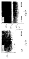
- FIG. 6 transmission electron microscopy (TEM) images of two such SLs are shown.
- TEM transmission electron microscopy
- a lattice-matched, nominally In0.53Ga0.47As layer grown on an InP substrate is shown in FIG. 6a .
- Clear ordering of the InGaAs layer 34 is seen with an ordering period of 5.4nm, while in the lower portion of the figure the uniform InP substrate 36 composition is apparent
- the ability to control the SL period is demonstrated in FIG.
- the layer structure for the RTD is nominally 2/1/2/1/2 nm AlAs/ In0.53Ga0.47As/InAs/In0.53Ga0.47As/AlAs; the light regions are the pseudomorphic AlAs tunneling barriers 38 .
- a doubling of the SL period is apparent as the rotation rate is switched from 5 rpm 40 to 2.5 rpm 42 .
- Resonant tunneling diodes RTDs
- RTDs Resonant tunneling diodes
- the effect of the rotation-induced SL on the transport properties of RTDs is to alter the conductance of the device over a narrow voltage range before or after the RTD transmission resonances. This phenomenon was observed in many RTDs before the origin of the effect was determined.
- composition modulated films When metals such as Cu, Ni, Cr, etc. are used as elemental sources instead of semiconductors, the same method of asymmetrically directing the source flux across the face of the substrate forms metal superlattice binary or ternary films also known as composition modulated films. Like semiconductor superlattices, the thickness of the composition modulated film layer is defined by the rotational speed and the growth rate. Composition modulated films result in a very finely dispersed structure that enhance the properties, for example, the mechanical strength, of a material.
Landscapes
- Chemical & Material Sciences (AREA)
- Engineering & Computer Science (AREA)
- Crystallography & Structural Chemistry (AREA)
- Materials Engineering (AREA)
- Metallurgy (AREA)
- Organic Chemistry (AREA)
- Nanotechnology (AREA)
- Mathematical Physics (AREA)
- Theoretical Computer Science (AREA)
- Physics & Mathematics (AREA)
- Physical Deposition Of Substances That Are Components Of Semiconductor Devices (AREA)
- Recrystallisation Techniques (AREA)
- Semiconductor Lasers (AREA)
Description
- This invention generally relates to the formation of rotation-induced superlattices.
- In molecular beam epitaxy (MBE), elemental source beams with cosinusoidal intensity profiles are directed across a vacuum space onto a heated substrate crystal 10. The substrate 10 is heated to provide sufficient energy for surface diffusion and incorporation of the species. The elemental source beams originate from separate ovens, often called effusion cells 12. The heated elements vaporize and exit the effusion cell 12 through one end, go past an
open shutter 14, and travel through thegrowth chamber 16 until reaching the substrate 10. Elements may be switched on and off using theshutter 14 in front of each effusion cell 12. FIG. 1 shows a schematic diagram of thegrowth chamber 16 of a prior art MBE machine. To compensate for the natural inhomogeneity of the beam intensity profiles and the necessarily nonsymmetric arrangement of sources within thegrowth chamber 16, the beams are not centered on the circular substrate 10, rather they are focused onto an intermediate point along the substrate radius. The substrate 10 is then rotated to achieve compositional uniformity. - To ensure uniformity, the rotation rate is chosen such that less than one monolayer is grown in the time it takes for a single substrate revolution. For a growth rate of 0.2 nm/s, compositional uniformity, both in the growth direction and radially across the substrate 10, requires rotation speeds of 60 rpm or more. However, practical considerations such as sample mounting, impurity control, and low maintenance growth procedures dictate a considerably lower substrate rotation speed, typically 2-10 rpm.
- A
superlattice 18, SL, is a one-dimensional periodic structure consisting of ultrathin layers 44, with its period less than the electron mean free path. A schematic of asuperlattice 18 is shown in FIG. 2. These ultra-thin layers 44 differ, in a prescribed manner, by their energy gaps. As the dimensions of the period become comparable to the electron wavelength, wave properties of the charge carriers become important. The energy profile of thesuperlattice 18 consists of alternating energy barriers as shown in FIG. 3. Classically, an electron with energy Ef, approaching an energy barrier with an energy below the barrier energy, Eb, would be reflected, analogous to a baseball rebounding off a concrete wall or to an electromagnetic wave at the end of an open-circuited transmission line. Quantum mechanics, however, allows that as the physical dimensions of the barrier decrease toward the wavelength of the particle, there is an increasing probability that the particles will be transmitted instead of reflected. Thus under certain conditions an electron can pass through the barrier even with energy below the barrier potential. This classically-forbidden phenomenon is called tunneling. Due to this phenomenon, some desirable aspects of superlattices are higher mobility and, lower electron scattering rates, translating into reduced parasitic resistance, and higher current gain in vertical devices such as heterojunction bipolar transistors (HBTs) and hot electron transistors. -
Superlattices 18 are obtained by a periodic variation of composition during epitaxial growth. Heretofore, in this field,superlattice structures 18 have been formed using mechanical shuttering in molecular beam epitaxy (MBE) growth. To introduce the periodic variation of composition, the elemental beam fluxes across the substrate 10 are varied by mechanically shuttering the effusion cells 12. This shuttering action, however, can cause growth transients and "shutter fatigue". Growth transients occur due to the pressure build up of the vaporized element in a closed effusion cell 12. Once the cell is opened again, a burst of atoms impinge upon the substrate 10, increasing the growth rate until the pressure has stabilized. "Shutter fatigue" occurs when theshutters 14 jam or don't open or close properly. Shutter 14 fatigue is especially common insuperlattice 18 growth due to the excessive number of transitions theshutters 14 must perform to fulfill the ultra-thin and multiple layer 44 requirements. - The materials currently of interest in superlattice growth are well-known semiconductors and their alloys; for examples, Ge, Si, Ge-Si alloys, III-V compounds and their alloys, II-VI compounds and their alloys, etc. InGaAs-InAlAs pseudomorphic and lattice-matched heterojunctions on InP substrates are of particular interest for use in high-performance transistor structures such as high electron mobility transistors (HEMTs), and resonant tunneling transistors (RTTs) because of the superior electron transport properties of InGaAs and the large conduction band offset (0.52eV obtained for the InGaAs/InAlAs heterojunction).
- The broad scope of this invention is intended to include any multi-deposition system, which by directing the elemental or molecular source fluxes across a substrate in an asymmetrical manner and rotating the substrate at low rotation speeds, forms a superlattice having a composition of A(x-Δx)B(1-(x-Δx))/A(x+Δx)B(1-(x+Δx) where Δx is a function of the nonuniform directing (which will be referred to in the following as "nonuniform focusing") of the elemental or molecular source fluxes A and B.
- More specifically, shutter fatigue and transient growth have been problems in the MBE formation of
superlattices 18. As a preferred embodiment, this invention describes an MBE method of forming asuperlattice 18 structure without the use ofshutters 14. This method is illustrated using a ternary and quaternary In(GaAl)As alloy on InP. By focusing theelemental beams substrate 26, asuperlattice 18 is formed having a composition of A(x-Δx)B(1-(x-Δx))As/A(x+Δx)B(1-(x+Δx)As where Δx is a function of the nonuniform focusing of theelemental beams A 22 andB 24, and, formation is obtained by rotating thesubstrate 26 at low rotation speeds. - In the drawings:
- FIG. 1 is a prior art schematic diagram of a molecular
beam epitaxy system 16. - FIG. 2 is a schematic diagram of a
superlattice structure 18. - FIG. 3 is an energy diagram of the forbidden and allowed energy zones in the conduction band of a superlattice.
- FIG. 4 is a schematic of the present invention wherein the
substrate 26, relative to the flux distribution in the MBE chamber, is rotated away from theuniform growth position 28. - FIG. 5 is a plot of the relationship between the compositional change in a
superlattice 18 versus the substrate's 26 angle of departure from auniform growth position 28 resulting from the use of this invention. - FIG. 6a is a cross-sectional view of a lattice-matched, nominally In0.53Ga0.47As SL layer grown on an InP substrate using the method of this invention.
- FIG. 6b is a cross-sectional view of a superlattice grown at a rotation rate of 2.5 rpm, a resonant tunneling diode structure, and a superlattice grown at a rotation rate of 5 rpm using the method of this invention.
- Corresponding numerals and symbols in the different figures refer to corresponding parts unless otherwise indicated.
- At low rotation speeds, 2-5 rpm, and typical growth rates of 0.1-0.3 nm/s, the layer composition in the grown film of the rotation-induced superlattice can be readily formed in conventional MBE systems. In the present invention, it's shown that the alloy composition variation is sufficient to form electrically active rotation-induced superlattices (SLs). As an example consider the growth of the ternary alloy In0.53Ga0.47As. If the intensities of the Ga and In beam profiles do not coincide, then the layer composition is alternatively In rich and Ga rich as the substrate is rotated through the nonuniform beams. Given a sufficient compositional variation, a strained layer SL is formed with a period equal to the layer thickness grown per substrate revolution. In this way, a rotation-induced superlattice is created with MBE without mechanical shuttering. In addition, superlattices may be formed using any other codeposition system, whereby at least two elemental sources are directed across the substrate. Another example of a codeposition system is a chemical beam epitaxy system. Further, alternative metallorganic chemical vapor deposition (MOCVD) or other vapor, liquid, or gas growth method can be used to form rotation-induced superlattices. In the preferred embodiment, depicted in FIG. 4, the growth system used is an MBE system (Riber-2300). Conventional thermal group III
sources InP substrates 26. The nominal growth temperature for InGaAs and AlAs is 460°C and 510°C, respectively, with V/III flux ratio of typically 2 to 3. Substrate rotation speeds are between 2 and 5 rpm. - Once the
InP substrate 26 is mounted, the substrate is tilted away from the normal MBE-uniform growth position 28 (near the co-focus point of alleffusion cells 22 and 24) such that all molecular beams focus at some point away from thesubstrate 26. Leaving alleffusion cells substrate 26 is rotated slowly(2-5 rpm). The nonuniform distribution of beam fluxes at the rotatingsubstrate 26 causes an ordering in the direction of growth with an ordering period determined by the product of growth rate and substrate rotation period. The effect of the ordering is to produce astrained layer SL 18 whose properties can be inferred from the current-voltage characteristics of resonant tunneling diodes. This strained layer superlattice has a pseudomorphic composition given by In(0.53-Δx)Ga(0.47+Δx)As/ In(0.53+Δx)Ga(0.47-Δx )As, whereby Δx is the difference in the maximum and minimum composition obtained in a single revolution. In(0.53)Ga(0.47)As is the composition corresponding to a lattice matching with InP. - The compositional variation Δx is determined by the angle of the substrate holder with respect to the uniform growth position. FIG. 4 shows the
substrate 26 relative to the flux distribution of the elemental sources A 22 andB 24 in the MBE chamber as thesubstrate 26 is rotated from theuniform growth position 28, θ=0, to a nonuniformflux distribution position 30, θ>0. As is illustrated in FIG. 5, as thesubstrate 26 is swung away from the growthdead center position 28, θ=0, there is a maximum composition difference at θ=θ1,position 30. As thesubstrate 26 is swung yet further away fromdead center position 28, the growth rate and the composition difference drops rapidly until there is no growth at θ=θ2,position 32. As this flux distribution is varied, the composition can be controlled and the superlattice performance can be uniquely defined for any application. - In the growth of the ternary and quaternary In(GaAl)As strained-layer SLs on InP, the period of the SL is determined by the layer thickness grown per substrate revolution. In FIG. 6, transmission electron microscopy (TEM) images of two such SLs are shown. A lattice-matched, nominally In0.53Ga0.47As layer grown on an InP substrate is shown in FIG. 6a. Clear ordering of the
InGaAs layer 34 is seen with an ordering period of 5.4nm, while in the lower portion of the figure theuniform InP substrate 36 composition is apparent The ability to control the SL period is demonstrated in FIG. 6b where, in the growth of a resonant tunneling diode structure, the rotation rate is doubled upon initiation of the resonant tunneling double-barrier growth. The layer structure for the RTD is nominally 2/1/2/1/2 nm AlAs/ In0.53Ga0.47As/InAs/In0.53Ga0.47As/AlAs; the light regions are the pseudomorphic AlAs tunnelingbarriers 38. A doubling of the SL period is apparent as the rotation rate is switched from 5rpm 40 to 2.5rpm 42. Resonant tunneling diodes (RTDs) are often formed in superlattices to enhance the electrical performance of the devices. The effect of the rotation-induced SL on the transport properties of RTDs is to alter the conductance of the device over a narrow voltage range before or after the RTD transmission resonances. This phenomenon was observed in many RTDs before the origin of the effect was determined. - When metals such as Cu, Ni, Cr, etc. are used as elemental sources instead of semiconductors, the same method of asymmetrically directing the source flux across the face of the substrate forms metal superlattice binary or ternary films also known as composition modulated films. Like semiconductor superlattices, the thickness of the composition modulated film layer is defined by the rotational speed and the growth rate. Composition modulated films result in a very finely dispersed structure that enhance the properties, for example, the mechanical strength, of a material.
Claims (18)
- A method of forming a superlattice structure having a selected layer thickness, comprising the steps of:mounting a substrate in a multi-deposition system on a rotating stage;providing individual elemental or molecular sources having individual growth rates;rotating the substrate such that the product of the rotation period times the source growth rate gives the selected layer thickness per superlattice period; anddirecting the elemental or molecular source fluxes in a nonuniform manner across the substrate to form a superlattice having a composition of A(x-Δx)B(1-(x-Δx))/A(x+Δx)B(1-(x+Δx)) wherein (x+Δx) <1 and >0, and Δx is the difference in the maximum and minimum composition obtained in a single revolution of the substrate by the nonuniform focusing of the elemental or molecular sources, A and B.
- A method of forming a superlattice structure having a selected layer thickness, comprising the steps of:mounting a substrate in a multi-deposition system on a rotating stage;providing individual elemental or molecular sources having individual growth rates;rotating the substrate such that the product of the rotation period times the source growth rate gives the selected layer thickness per superlattice period; anddirecting the elemental or molecular source fluxes in a nonuniform manner across the substrate to form a superlattice comprised of ternary alloys and has a composition of A(x-Δx)B(1-(x-Δx))C/A(x+Δx)B(1-(x+Δx))C, where C is selected from the group consisting of As, P and Sb and is a constant and wherein (x+Δx) <1 and >0, and Δx is the difference in the maximum and minimum composition obtained in a single revolution of the substrate by the nonuniform focusing of the elemental or molecular sources, A and B.
- A method of forming a superlattice structure having a selected layer thickness, comprising the steps of:mounting a substrate in a multi-deposition system on a rotating stage;providing individual elemental or molecular sources having individual growth rates;rotating the substrate such that the product of the rotation period times the source growth rate gives the selected layer thickness per superlattice period; anddirecting the elemental or molecular source fluxes in a nonuniform manner across the substrate to form a superlattice comprised of quaternary or multiconsituent in composition and produced by rotation through nonuniform source fluxes and having a composition A(x-Δx)B(1-(x-Δx))/Ax+Δx)B(1-(x+Δx)) wherein (x+Δx) <1 and >0, and Δx is the difference in the maximum and minimum composition obtained in a single revolution of the substrate by the nonuniform focusing of the elemental or molecular sources, A and B.
- The method of claim 1, wherein said multi-depositional system is a molecular beam epitaxy system.
- The method of claim 1, further comprising the steps of:providing effusion cells;providing said individual elemental or molecular sources in said effusion cells; andheating the effusion cells until the sources vaporize.
- The method of claim 1, wherein said multi-depositional system is a chemical deposition epitaxy system.
- The method of claim 1, wherein said multi-depositional system is a gas source epitaxy system.
- The method of claim 1, wherein said substrate is of a material selected from the group consisting of Si, InP, GaAs, CdTe, GaSb, and AlSb.
- The method of claim 2, wherein said individual elemental or molecular sources are selected from group III elements.
- The method of claim 2, wherein said ternary alloy consists of As and two of the three elements Ga, In and Al.
- The method of claim 1, wherein said rotation speed is between about 1-5 rpm and the growth rate is 0.1-0.2 nanometers second.
- The method of claim 1, wherein for a semiconductor superlattice, said product of the rotation period times the growth rate is of the order of the electron wavelength.
- The method of claim 1, wherein said individual elemental or molecular sources are selected from group IV elements.
- The method of claim 1, wherein said individual elemental or molecular sources are selected from group II and group VI.
- The method of claim 1, wherein said focusing said elemental or molecular source fluxes in a nonuniform manner comprises offsetting the elemental or molecular sources from a co-focus position.
- The method of claim 1, wherein said focusing said elemental or molecular source fluxes in a nonuniform manner comprises tilting the sample away from a co-focus point of all elemental or molecular sources.
- The method of claim 2, wherein said A(x-Δx)B(1-(x-Δx))C/A(x+Δx)B(1-(x+Δx))C is In(0.53-Δx) Ga(0.47+Δx)As/In(0.53+Δx)Ga(0.47-Δx)As.
- The method of claim 1, wherein said Δx is zero resulting in a lattice matched composition.
Applications Claiming Priority (2)
| Application Number | Priority Date | Filing Date | Title |
|---|---|---|---|
| US68394291A | 1991-04-12 | 1991-04-12 | |
| US683942 | 1991-04-12 |
Publications (3)
| Publication Number | Publication Date |
|---|---|
| EP0508463A2 EP0508463A2 (en) | 1992-10-14 |
| EP0508463A3 EP0508463A3 (en) | 1993-02-03 |
| EP0508463B1 true EP0508463B1 (en) | 1997-07-02 |
Family
ID=24746088
Family Applications (1)
| Application Number | Title | Priority Date | Filing Date |
|---|---|---|---|
| EP92106256A Expired - Lifetime EP0508463B1 (en) | 1991-04-12 | 1992-04-10 | Method of forming a rotation-induced superlattice structure |
Country Status (4)
| Country | Link |
|---|---|
| US (1) | US5415128A (en) |
| EP (1) | EP0508463B1 (en) |
| JP (1) | JPH05114768A (en) |
| DE (1) | DE69220600T2 (en) |
Families Citing this family (6)
| Publication number | Priority date | Publication date | Assignee | Title |
|---|---|---|---|---|
| US5514876A (en) * | 1994-04-15 | 1996-05-07 | Trw Inc. | Multi-terminal resonant tunneling transistor |
| US5616180A (en) * | 1994-12-22 | 1997-04-01 | Northrop Grumman Corporation | Aparatus for varying the flux of a molecular beam |
| US6217937B1 (en) | 1998-07-15 | 2001-04-17 | Cornell Research Foundation, Inc. | High throughput OMVPE apparatus |
| EP1588406B1 (en) * | 2003-01-27 | 2019-07-10 | Taiwan Semiconductor Manufacturing Company, Ltd. | Semiconductor structures with structural homogeneity |
| JP3964367B2 (en) * | 2003-08-25 | 2007-08-22 | シャープ株式会社 | Molecular beam epitaxial growth apparatus and control method thereof |
| US9127349B2 (en) * | 2008-12-23 | 2015-09-08 | Applied Materials, Inc. | Method and apparatus for depositing mixed layers |
Family Cites Families (10)
| Publication number | Priority date | Publication date | Assignee | Title |
|---|---|---|---|---|
| JPS60145998A (en) * | 1984-01-07 | 1985-08-01 | Agency Of Ind Science & Technol | Mbe growth method |
| GB2158843A (en) * | 1984-05-14 | 1985-11-20 | Philips Electronic Associated | Method of manufacturing a semiconductor device by molecular beam epitaxy |
| JPS61181121A (en) * | 1985-02-06 | 1986-08-13 | Sumitomo Electric Ind Ltd | Manufacture of semiconductor thin film |
| JPS61278130A (en) * | 1985-06-04 | 1986-12-09 | Fujitsu Ltd | Molecular-beam epitaxial growth device |
| KR900002687B1 (en) * | 1985-12-16 | 1990-04-23 | 후지쓰가부시끼가이샤 | Method for growing 4-membered or 5-membered semiconducting semiconductors lattice matched to a substrate by MBE |
| US4885260A (en) * | 1987-02-17 | 1989-12-05 | Matsushita Electric Industrial Co., Ltd. | Method of laser enhanced vapor phase growth for compound semiconductor |
| EP0305195A3 (en) * | 1987-08-27 | 1990-11-28 | Texas Instruments Incorporated | Continuous chemical vapor deposition growth of strain layer superlattices using conventional cvd reactors |
| JP2650930B2 (en) * | 1987-11-24 | 1997-09-10 | 株式会社日立製作所 | Superlattice device fabrication method |
| JPH01278496A (en) * | 1988-04-28 | 1989-11-08 | Shimadzu Corp | Thin film manufacturing method |
| US5091335A (en) * | 1990-03-30 | 1992-02-25 | The United States Of America As Represented By The Administrator Of The National Aeronautics And Space Administration | MBE growth technology for high quality strained III-V layers |
-
1992
- 1992-04-10 JP JP4091163A patent/JPH05114768A/en active Pending
- 1992-04-10 EP EP92106256A patent/EP0508463B1/en not_active Expired - Lifetime
- 1992-04-10 DE DE69220600T patent/DE69220600T2/en not_active Expired - Fee Related
-
1994
- 1994-03-09 US US08/209,693 patent/US5415128A/en not_active Expired - Fee Related
Also Published As
| Publication number | Publication date |
|---|---|
| DE69220600D1 (en) | 1997-08-07 |
| EP0508463A3 (en) | 1993-02-03 |
| JPH05114768A (en) | 1993-05-07 |
| EP0508463A2 (en) | 1992-10-14 |
| DE69220600T2 (en) | 1998-01-02 |
| US5415128A (en) | 1995-05-16 |
Similar Documents
| Publication | Publication Date | Title |
|---|---|---|
| US6218677B1 (en) | III-V nitride resonant tunneling | |
| US4845049A (en) | Doping III-V compound semiconductor devices with group VI monolayers using ALE | |
| Tsang et al. | Molecular beam epitaxial growth of In1− xGaxAs1− ySby lattice matched to GaSb | |
| EP0229263B1 (en) | Method of growing quaternary or pentanary compound semiconductor by mbe lattice-matched to substrate | |
| JPH01128577A (en) | Semiconductor device | |
| JPH06204499A (en) | Pn junction device having group IV element-doped III-V compound semiconductor | |
| US5723872A (en) | Mixed barrier resonant tunneling | |
| US5415128A (en) | Rotation induced superlattice | |
| US4398963A (en) | Method for making non-alloyed heterojunction ohmic contacts | |
| Dmitriev et al. | InAlAs/InGaAs/InP heterostructures for microwave photodiodes grown by molecular beam epitaxy | |
| Chu et al. | Hg1− x Mn x Te‐CdTe superlattices grown by molecular beam epitaxy | |
| JPH0661270A (en) | Semiconductor device manufacturing method and semiconductor device | |
| Zhang et al. | Improved crystalline quality of AlAs x Sb1− x grown on InAs by modulated molecular‐beam epitaxy | |
| Pamulapati et al. | The relation of the performance characteristics of pseudomorphic In0. 53+ x Ga0. 47− x As/In0. 52Al0. 48As (0≤ x≤ 0.32) modulation‐doped field‐effect transistors to molecular‐beam epitaxial growth modes | |
| US8242538B1 (en) | Method and device for growing pseudomorphic A1InAsSb on InAs | |
| Arpapay et al. | The role of antiphase domain boundary density on the surface roughness of GaSb epilayers grown on Si (001) substrates | |
| Ploog | Molecular Beam Epitaxy of Artificially Layered III-V Semiconductors: Ultrathin-Layer (GaAs) m (AlAs) m Superlattices and Delta (δ-) Doping in GaAs | |
| JP2557373B2 (en) | Compound semiconductor device | |
| Henini | Molecular beam epitaxy: from research to manufacturing | |
| Hafich et al. | Gas‐source molecular‐beam epitaxy growth of In x Ga1− x− y Al y P | |
| US12132137B2 (en) | Continuous compositional grading for realization of low charge carrier barriers in electro-optical heterostructure semiconductor devices | |
| GB2219130A (en) | A high mobility semiconductor device | |
| JPH0513328A (en) | Mixed crystal semiconductor device and manufacturing method thereof | |
| EP0697741A1 (en) | Resonant tunneling devices | |
| JP2576232B2 (en) | Semiconductor crystal |
Legal Events
| Date | Code | Title | Description |
|---|---|---|---|
| PUAI | Public reference made under article 153(3) epc to a published international application that has entered the european phase |
Free format text: ORIGINAL CODE: 0009012 |
|
| AK | Designated contracting states |
Kind code of ref document: A2 Designated state(s): DE FR GB IT NL |
|
| PUAL | Search report despatched |
Free format text: ORIGINAL CODE: 0009013 |
|
| AK | Designated contracting states |
Kind code of ref document: A3 Designated state(s): DE FR GB IT NL |
|
| 17P | Request for examination filed |
Effective date: 19930721 |
|
| 17Q | First examination report despatched |
Effective date: 19950112 |
|
| GRAG | Despatch of communication of intention to grant |
Free format text: ORIGINAL CODE: EPIDOS AGRA |
|
| GRAH | Despatch of communication of intention to grant a patent |
Free format text: ORIGINAL CODE: EPIDOS IGRA |
|
| GRAH | Despatch of communication of intention to grant a patent |
Free format text: ORIGINAL CODE: EPIDOS IGRA |
|
| GRAA | (expected) grant |
Free format text: ORIGINAL CODE: 0009210 |
|
| AK | Designated contracting states |
Kind code of ref document: B1 Designated state(s): DE FR GB IT NL |
|
| REF | Corresponds to: |
Ref document number: 69220600 Country of ref document: DE Date of ref document: 19970807 |
|
| ET | Fr: translation filed | ||
| PLBE | No opposition filed within time limit |
Free format text: ORIGINAL CODE: 0009261 |
|
| STAA | Information on the status of an ep patent application or granted ep patent |
Free format text: STATUS: NO OPPOSITION FILED WITHIN TIME LIMIT |
|
| 26N | No opposition filed | ||
| NLS | Nl: assignments of ep-patents |
Owner name: RAYTHEON COMPANY |
|
| REG | Reference to a national code |
Ref country code: GB Ref legal event code: 732E |
|
| REG | Reference to a national code |
Ref country code: GB Ref legal event code: IF02 |
|
| PGFP | Annual fee paid to national office [announced via postgrant information from national office to epo] |
Ref country code: FR Payment date: 20020311 Year of fee payment: 11 |
|
| PGFP | Annual fee paid to national office [announced via postgrant information from national office to epo] |
Ref country code: GB Payment date: 20020313 Year of fee payment: 11 |
|
| PGFP | Annual fee paid to national office [announced via postgrant information from national office to epo] |
Ref country code: DE Payment date: 20020314 Year of fee payment: 11 |
|
| PGFP | Annual fee paid to national office [announced via postgrant information from national office to epo] |
Ref country code: NL Payment date: 20030325 Year of fee payment: 12 |
|
| PG25 | Lapsed in a contracting state [announced via postgrant information from national office to epo] |
Ref country code: GB Free format text: LAPSE BECAUSE OF NON-PAYMENT OF DUE FEES Effective date: 20030410 |
|
| PG25 | Lapsed in a contracting state [announced via postgrant information from national office to epo] |
Ref country code: DE Free format text: LAPSE BECAUSE OF NON-PAYMENT OF DUE FEES Effective date: 20031101 |
|
| GBPC | Gb: european patent ceased through non-payment of renewal fee |
Effective date: 20030410 |
|
| PG25 | Lapsed in a contracting state [announced via postgrant information from national office to epo] |
Ref country code: FR Free format text: LAPSE BECAUSE OF NON-PAYMENT OF DUE FEES Effective date: 20031231 |
|
| REG | Reference to a national code |
Ref country code: FR Ref legal event code: ST |
|
| PG25 | Lapsed in a contracting state [announced via postgrant information from national office to epo] |
Ref country code: NL Free format text: LAPSE BECAUSE OF NON-PAYMENT OF DUE FEES Effective date: 20041101 |
|
| NLV4 | Nl: lapsed or anulled due to non-payment of the annual fee |
Effective date: 20041101 |
|
| PG25 | Lapsed in a contracting state [announced via postgrant information from national office to epo] |
Ref country code: IT Free format text: LAPSE BECAUSE OF NON-PAYMENT OF DUE FEES Effective date: 20050410 |