EP0508151A1 - Charged particle beam exposure system and charged particle beam exposure method - Google Patents
Charged particle beam exposure system and charged particle beam exposure method Download PDFInfo
- Publication number
- EP0508151A1 EP0508151A1 EP92104354A EP92104354A EP0508151A1 EP 0508151 A1 EP0508151 A1 EP 0508151A1 EP 92104354 A EP92104354 A EP 92104354A EP 92104354 A EP92104354 A EP 92104354A EP 0508151 A1 EP0508151 A1 EP 0508151A1
- Authority
- EP
- European Patent Office
- Prior art keywords
- charged particle
- blanking
- exposed
- blanking aperture
- particle beam
- Prior art date
- Legal status (The legal status is an assumption and is not a legal conclusion. Google has not performed a legal analysis and makes no representation as to the accuracy of the status listed.)
- Granted
Links
Images


Classifications
-
- H—ELECTRICITY
- H01—ELECTRIC ELEMENTS
- H01J—ELECTRIC DISCHARGE TUBES OR DISCHARGE LAMPS
- H01J37/00—Discharge tubes with provision for introducing objects or material to be exposed to the discharge, e.g. for the purpose of examination or processing thereof
- H01J37/30—Electron-beam or ion-beam tubes for localised treatment of objects
- H01J37/317—Electron-beam or ion-beam tubes for localised treatment of objects for changing properties of the objects or for applying thin layers thereon, e.g. for ion implantation
- H01J37/3174—Particle-beam lithography, e.g. electron beam lithography
- H01J37/3177—Multi-beam, e.g. fly's eye, comb probe
-
- B—PERFORMING OPERATIONS; TRANSPORTING
- B82—NANOTECHNOLOGY
- B82Y—SPECIFIC USES OR APPLICATIONS OF NANOSTRUCTURES; MEASUREMENT OR ANALYSIS OF NANOSTRUCTURES; MANUFACTURE OR TREATMENT OF NANOSTRUCTURES
- B82Y10/00—Nanotechnology for information processing, storage or transmission, e.g. quantum computing or single electron logic
-
- B—PERFORMING OPERATIONS; TRANSPORTING
- B82—NANOTECHNOLOGY
- B82Y—SPECIFIC USES OR APPLICATIONS OF NANOSTRUCTURES; MEASUREMENT OR ANALYSIS OF NANOSTRUCTURES; MANUFACTURE OR TREATMENT OF NANOSTRUCTURES
- B82Y40/00—Manufacture or treatment of nanostructures
-
- H—ELECTRICITY
- H01—ELECTRIC ELEMENTS
- H01J—ELECTRIC DISCHARGE TUBES OR DISCHARGE LAMPS
- H01J37/00—Discharge tubes with provision for introducing objects or material to be exposed to the discharge, e.g. for the purpose of examination or processing thereof
- H01J37/02—Details
- H01J37/04—Arrangements of electrodes and associated parts for generating or controlling the discharge, e.g. electron-optical arrangement, ion-optical arrangement
- H01J37/09—Diaphragms; Shields associated with electron or ion-optical arrangements; Compensation of disturbing fields
-
- H—ELECTRICITY
- H01—ELECTRIC ELEMENTS
- H01J—ELECTRIC DISCHARGE TUBES OR DISCHARGE LAMPS
- H01J2237/00—Discharge tubes exposing object to beam, e.g. for analysis treatment, etching, imaging
- H01J2237/04—Means for controlling the discharge
- H01J2237/043—Beam blanking
- H01J2237/0435—Multi-aperture
Definitions
- the present invention relates to a charged particle beam exposure system that is adapted to continuously scan a number of charged particle beams with a blanking aperture array having a number of rows of open holes.
- ICs have been expected to advance in terms of integration density and function as core technology for technological progress of industrial fields including computers, mechanical control, communications, etc.
- ICs have reached a four-fold level of high integration within the last three or four years.
- the integration density of the DRAM has increased from 1M through to 4M, 16M, 64M, 256M and 1G.
- Said high integration development has depended solely on the advancement of precision fabrication technology, particularly the advancement of optical technology that allows precision operations in 0.5 ⁇ m units.
- the precision limit of optical technology is approximately 0.3 ⁇ m and it is becoming difficult to maintain a precision of 0.10 ⁇ m in windowing for contact holes and alignment with a pattern of a lower layer. Since a pellicle cannot be applied to a mask in the case of X-ray exposure and a defect-free guarantee is difficult, X-ray exposure cannot be used in the fabrication of LSIs that are required to provide high reliability.
- the most popular type of charged particle beam exposure system is the point beam raster scan exposure system. However, in this system, only one beam is used and the throughput is extremely low and therefore the exposure of wafers is impossible in the volume production level.
- variable square beam system a limited size of square can be formed by one shot and therefore a satisfactory throughput can be obtained with a rough pattern; the smallest pattern of which is approximately 2 ⁇ m. Accordingly, this system can be used for direct exposure production of small lots of products.
- LSIs of high pattern density cannot overcome the restriction of a one-writing pattern and cannot avoid an extremely low throughput.
- a system for transferring a repetitive memory pattern as a contraction image of charged particle beams passing through a silicon stencil mask is referred to as the block exposure system.
- This block exposure system allows volume production of memory chips of 256M and 1G by repeatedly irradiating a pattern, which is often used for the memory at a high repetition rate.
- the block exposure system has the vital defect that the throughput for a random pattern is extremely low as in case of the variable square beam.
- Most gate arrays and micro computers are often based on random patterns.
- FIG. 14 shows an example of a configuration of the prior art blanking aperture array, and this blanking aperture array 6 is provided with a row of openings 62 that are a plural number of apertures arranged in a line.
- An ON or OFF signal from the beam ON/OFF signal generator 33 is entered independently into the electrode 61 provided at an inside surface of each opening 62 through circuit lines l 1 , l 2 , ... l n and a constant voltage (for example, a ground potential) is applied to the electrode 63 provided at the other inside surface of opening 62 through a common line.
- a plurality of beams passing through the openings 62 are arranged in a line and these blanking apertures 62 are ON/OFF controlled by an appropriate control means.
- the system is adapted so that the charged particle beams that have passed through the blanking apertures 62, into which the ON signal is entered, reach the specified point on the surface of object to be exposed and the specified point is exposed and the charged particle beams that have passed through the blanking apertures 62 into which the OFF signal is entered, is interrupted by an appropriate shield plate and prevented from reaching the surface of object to be exposed. Then a specified pattern is exposed as if it is scraped with a brush while scanning a plurality of charged particle beams obtained by the above described ON/OFF control.
- the second problem is a sensitivity of resists. Electrons are particles and the number of electrons that are incident into a unit area within a unit time varies in terms of the Poisson's distribution and therefore the resolution is basically in inverse proportion to a square root of the sensitivity. Accordingly, if the smallest pattern is 0.2 ⁇ m, a resist with the sensitivity of 5 - 10 ⁇ C/cm 2 is generally required. A high sensitivity resist has only a low resolution and the system for which implementation of high sensitivity is excessively expected cannot be used in actual volume production of LSIs.
- the throughput of 1 cm 2 /sec is a target value for the resist sensitivity of 5 - 10 ⁇ C/cm 2
- the required overall current is 5 - 10 ⁇ A.
- Another beam size is assumed as 0.05 ⁇ m ⁇ on the surface of a specimen.
- the overall current value of 1600 beams is 10 ⁇ A.
- a coulombic interaction has been considered a physical bottleneck for the charged particle beams.
- This coulombic interaction is a phenomenon such that the beams become dim because of interactive repulsion of electrons.
- the main cause of this phenomenon is that the focal distance is extended because of interactive repulsion of charged particle beams in proportion to the current value of overall electron flow in the lens near the surface of specimen (in other words, in proportion to the number of charged particle beams in the ON state) and the focal point deviates downward from the specimen surface (that is, the surface of wafer 19) as shown in Figure 7 (B).
- numeral 8 denotes the charged particle beam in the ON state and numerals 12 and 17 denote the electron lens for focusing shown in Figure 12.
- the focal deviation due to such coulombic interaction scarcely takes place when the number of charged particle beams 8 in the ON state is small as shown in Figure 7 (A) but occurs when the number of charged particle beams 8 in the ON state is large (the maximum number of beams reaches, for example, 1600 as described above) as shown in Figure 7 (B).
- the focal deviation because of said coulombic interaction can be corrected by providing a small refocus coil (for example, approximately 4 mm in diameter) at a position near the peak of the magnetic field in the final stage lens or the preceding lens (that is, a position where the magnetic field is most intensified) and supplying a refocus current in proportion to the current value of all charged particle beams (that is, the number of charged particle beams that remain in the ON state at that time) to the refocus coil at the rate of, for example, 50 nsec (50 + 1 sec).
- a small refocus coil for example, approximately 4 mm in diameter
- the rate of approximately 50 nsec is the limit of the response speed of the amplifier (analog current-driven type amplifier) for supplying the specified refocus current to the refocus coil in accordance with the number of charged particle beams that remain in the ON state at that time.
- the beam dwell time per 0.05 ⁇ m is 2.5 nsec. Since such line beams are scanned at a high speed, it is necessary to vary the refocus current (for example, approximately 1A, maximum) in steps (for example, 0A to 1A) within a time far shorter than 2.5 nsec, which is the beam dwell time at the above-described point at the boundary between the exposure of a completely written-out region and the partially exposed region.
- An intermediate color cannot be represented with the conventional line beams and a pattern of dimensions as large as an integral multiple of the dimensions of a single beam cannot be formed. Though such pattern can be formed by plural times of movement of the stage or beam scanning, the throughput is extremely low and volume production cannot be carried out.
- the exposure efficiency with the charged particle beams can be improved by using said blanking aperture array, whereas a resist that provides a higher resolution should be used in accordance with the degree of precision of a pattern to be exposed and therefore the exposure time becomes longer and the throughput is reduced.
- the exposure should be carried out through the blanking apertures that are arranged as close to each other as possible to prevent such defects as deformation or discontinuity of the pattern or the like.
- the charged particle beams have a fixed intensity distribution as described above and therefore there is the so-called proximity effect that adjacent charged particle beams interfere with each other and the pattern is exposed beyond the predetermined amount of irradiation.
- such adjustment has been difficult in the conventional blanking aperture array.
- Some examples of two-dimensional arrangement of the groups of blanking apertures in the above described blanking aperture array unit have been known to solve the above problems.
- all charged particle beams forming the specified pattern passing through the blanking aperture array unit are simultaneously irradiated onto the specified position of an object to be exposed to carry out an exposure process and subsequently all charged particle beams formed in the same or different pattern are simultaneously irradiated onto an adjacent object to be exposed to carry out the exposure processing.
- a high speed pattern forming method is disclosed by USP 4153843 in which a blanking aperture array provided with a plurality of blanking apertures arranged in two dimensional form is used and thus a plurality of charged particle electron beams are radiated on a surface of a sample to be exposed to the beam to form a predetermined pattern thereon and wherein a total amount of radiation value at a certain addressed position of the sample to which,a respective charged particle electron beam is to be exposed.
- each one of the charged particle electron beams formed by each one of the apertures A, B, and C forming a first aperture line arranged parallel to a scanning direction Y of the charged particle electron beams radiates each one of addressed positions of the sample forming one line 1 arranged parallel to the scanning direction Y of the charged particle electron beams and each one of the charged particle electron beams formed by each one of the apertures B, E, and H forming a second aperture line arranged parallel to a scanning direction Y thereof, radiates each one of addressed positions of the sample forming another line 6 arranged parallel to the scanning direction Y and while each one of the charged particle electron beams formed by each one of the apertures C, F, and I forming a third aperture line arranged parallel to a scanning direction Y thereof, radiates each one of addressed positions of the sample forming another line 11 arranged parallel to the scanning direction Y.
- the charged particle electron beams formed by apertures forming respective lines radiate addressed positions formed on any one of the lines on the sample, and each line is separated a predetermined space from each other.
- the spaced addressed positions are successively radiated by each one of the charged particle electron beams formed by each one of the aperture lines formed in the aperture array and thereby all addressed positions are ultimately fully exposed; this method is generally called an interleave method.
- the charged particle electron beams formed by the aperture A exposes sequentially continuously arranged addressed positions to form in turn a line on the samples, (1, a), (1, b), (1, c) ... (1, 1), (2, 1), (2, k), ... (2, a), (3, a), (3, b), ... (3, 1).
- the charged particle electron beams formed by the aperture B exposes sequentially continuously arranged addressed positions to form in turn a line on the samples, (6, a), (6, b), (6, c) ... (6, 1), (7, 1), (7, k), ... (7, a), (8, a), (8, b), ... (8, 1).
- the charged particle electron beams formed by the aperture C exposes sequentially continuously arranged addressed positions to form in turn a line on the samples (11, a), (11, b), (11, c) ... (11, 1), (12, 1), (12, k), ... (12, a), (13, a), (13, b), ... (13, 1).
- the characteristic feature of the conventional technology is such that a plurality of addressed positions formed on the sample, each of them being separated a predetermined distance from each other, are simultaneously and respectively exposed to different charged particle electron beams in a predetermined exposed region.
- the charged particle electron beams formed by the apertures D and G in the first apertures line formed by the apertures A, D, and G expose the same addressed position to which the charged particle electron beam formed by the aperture A exposes successively with a predetermined time difference. Therefore, in the embodiment as shown in Fig. 20, one of the addressed positions in the sample to be exposed will be exposed three times by the charged particle electron beam and therefore, a dose value of the same addressed position caused by the exposure of the beams can be optionally changed by changing the exposure number within 3 times.
- the conventional technology discloses that each of the charged particle electron beams exposes each one of the addressed positions respectively and thus control of the beam is difficult.
- a predetermined time should be required from the time when the beams have exposed one addressed position to the time when the same beams expose another adjacent addressed position.
- a light sensitive layer formed at a predetermined addressed position is affected by another beam that exposes another addressed position next to the predetermined addressed position, and thus in the conventional technology, since the exposure time is different, the exposed condition of the sensitive layer of one addressed position will change as time elapses.
- An object of the present invention is to provide a means for solving the various above described problems in the exposure method by the conventional line beams, particularly a charged particle beam exposure system capable of easily correcting the focal deviation of charged particle beams due to the above described coulombic interaction to allow the formation of a sharp pattern when any type of exposure pattern is used and the number of charged particle beams is increased and appropriately varies the amount of irradiation of charged particle beams for each pattern; thereby the proximity effect can be prevented and a pattern having a desired exposure condition can be efficiently formed.
- the primary object of the present invention is to obtain a charged particle beam exposure system in which line connections to the electrodes on the blanking aperture array are easy.
- the present invention for solving the above described problems is to provide a method for exposing a charged particle beam and a charged particle beam exposure system of a configuration as described below.
- a method for exposing a charged particle beam to an object to be exposed with a charged particle beam exposure system comprising, a charged particle beam generating means for generating a charged particle beam, a blanking aperture array means for shaping said charged particle beam generated by said charged particle beam generating means and having a plurality of blanking apertures arranged in two dimensional form, a stage means for holding an object to be exposed, a deflection means for deflecting the charged particle beam passing through said blanking aperture array means by a specified amount in order to irradiate the charged particle beams onto a specified position of said object to be exposed, wherein said method comprising the steps of, a first step of irradiating a pattern formed by said charged particle beams arranged in two dimensional configuration on a first region specified on said object to be exposed, a second step of successively irradiating the pattern formed by said charged particle beams arranged in two dimensional configuration on a second region having an overlapping region in which at least a portion of said second region and at least
- a group of charged particle beams having a specified pattern that have passed a plurality of blanking apertures two-dimensionally arranged are not simultaneously irradiated onto the specified position of the object to be exposed unlike the prior art system and part of the specified pattern to which the specified position of the object is exposed is divided and irradiated a plurality of times.
- the charged particle beams to be irradiated onto the specified position of the object to be exposed are supplied through different blanking apertures, respectively.
- the unit exposure points that form a pattern on the object to be exposed overlap and are irradiated as many times as specified with the above described plurality of charged particle beams.
- the blanking aperture array control unit is constructed so that the same pattern as the specified pattern to be exposed to the charged particle beams or the same pattern as at least part of the specified pattern is formed with the groups of blanking apertures that remain in the ON state at a specified region of the object to be exposed and the specified pattern is moved on the blanking aperture array in the specified direction while synchronized with the deflection scanning of the charged particle beams.
- Movement of the pattern on the blanking aperture array and deflection scanning of the charged particle beams by means of electromagnetic deflection are controlled by an appropriate control means so that the charged particle beams are irradiated onto the same position of the object to be exposed even when the charged particle beams forming part of a special pattern by exposure pass through different apertures of the blanking apertures on which the pattern moves.
- the construction is such that the specified region of the object to be exposed is exposed, in a specified pattern, to the charged particle beams passing through the specified blanking apertures of the blanking aperture array that remain in the ON state when the charged particle beams are scanned by the electromagnetic deflection means, and the specified position and the ambient part of the object to be exposed overlap and are irradiated in sequence with a plurality of charged particle beams that have passed through different blanking apertures at a specified time interval when the blanking aperture array control unit controls the movement of the specified pattern, which is formed on the blanking aperture array, in one direction.
- the amount of irradiation necessary for the resist provided on the object to be exposed to completely form a pattern is divided a plurality of times (n times) when forming the specified pattern to be formed on the object to be exposed, and therefore the intensity of the charged particle beams irradiated at one time is 1/n of the amount of irradiation generally required for forming the pattern.
- the charged particle beams are scanned and irradiated in sequence in, for example; the stage direction of the groups of blanking apertures provided on the blanking aperture array, and therefore the variation of electrons due to the groups of charged particle beams that change at a time, is far smaller than the whole blanking aperture array and there is no possibility of the refocus problem occurring.
- the charged particle beams for forming a specific part of the specified pattern pass through the blanking apertures, which are individually controlled and, at the same time, the charged particle beams supplied from different blanking apertures overlap and are irradiated in sequence onto the same position of the object to be exposed at a specified time interval.
- the number of overlapping irradiation can be freely changed by changing over the ON state of the specified blanking apertures to the OFF state to reduce the number of times of irradiating operations and the disadvantages associated with the prior art can be eliminated.
- the speed of an irradiating operation is substantially increased since the intensity of charged particle beams required to form each pattern can be reduced and,the construction of the apparatus can be small since the configuration of the control stages can be simplified.
- the groups of blanking apertures provided on the blanking aperture array are arranged in a checkered pattern so that, for example, the first aperture stage and the second aperture stage do not contact each other and therefore, even when there are many groups of apertures, line connection to the electrodes provided on the blanking apertures is easy and the specified pattern of the object to be exposed can be exposed without clearance and in a coordinate direction orthogonally intersecting the scanning direction with the charged particle beams passing through the first row of openings and the charged particle beams passing through the second row of openings of the groups of blanking apertures.
- Figure 1 is a diagram showing the basic configuration of the blanking aperture array used in the present invention.
- Figure 2 is a diagram showing another configuration of the blanking aperture array used in the present invention.
- Figure 3 is a diagram showing a further another configuration of the blanking aperture array used in the present invention.
- Figures 4 (A) and 4 (B) are respectively a diagram showing the relationship between an example of main deflection and sub-deflection of the charged particle beams and the direction of the blanking aperture stage of the blanking aperture array means in accordance with the present invention and Figure 4 (C) is a diagram showing the scanning waveforms of charged particle beams in the sub-deflection direction (Y direction).
- Figure 5 is a diagram illustrating the principle of the exposure method in the charged particle beam exposure system in accordance with the present invention.
- Figure 6 is a diagram illustrating the principle of the exposure method in the charged particle beam exposure system in accordance with the present invention.
- Figure 7 is a diagram illustrating the function of the refocus.
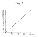
- Figure 8 is a diagram illustrating the output current waveforms supplied to the refocus coil.
- Figure 9 is a diagram showing an example of a proximity effect correction by the exposure method in accordance with the present invention.
- Figure 10 is an explanatory diagram for forming an exposure pattern shifted by a smaller size than the beam size according to the exposure method of the present invention.
- Figure 11 is an explanatory diagram for exposing the stitch of the fields or the, sub-fields by the exposure method of the present invention.
- Figure 12 is a diagram showing an example of the overall configuration of the charged particle beam exposure system in which the method in accordance with the present invention is to be embodied.
- Figure 13 is a circuit connection diagram of the electrical system to be connected to the sections of the apparatus shown in Figure 12.
- Figure 14 is a diagram showing an example of the configuration of the prior art blanking aperture array.
- Figure 15 is a diagram describing an exposure problem using the prior art blanking aperture array.
- Figure 16 is a diagram illustrating a practical example of another exposure method for the charged particle beam exposure system in accordance with the present invention.
- Figure 17 is a diagram illustrating an example of line connections of the prior art blanking aperture array.
- Figure 18 is a diagram illustrating an example of line connection-pattern to the blanking electrodes in the blanking aperture array shown in Figure 1.
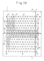
- Figure 19 is a diagram showing an example of connection of the constant voltage applying circuit to the blanking electrodes in the blanking aperture array shown in Figure 1.
- Figure 20 shows a conventional exposure method.
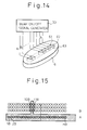
- Figure 12 is a diagram that exemplifies the overall configuration of the charged particle exposure system related to the present invention.
- the electron gun 1 comprises a cathode 2 composed of LaB 6 and others, a grid 3 and an anode 4.
- Numerals 5, 7, 10, 12, 17 and 21 respectively denote electron lenses for convergence and a blanking aperture array 6 construction as described later is provided in the electron lens 7.
- Numeral 8 denotes the so-called ON beam, which passes through the blanking aperture to the electrode of which an ON signal is applied among the blanking apertures provided in the blanking aperture array 6 and is irradiated onto the specified point on the object (wafer surface) 19 to be exposed.
- Numeral 9 denotes the so-called OFF beam, which passes through the blanking aperture to the electrode of which an OFF signal is applied among the blanking apertures provided in the blanking aperture array 6 and is interrupted by an appropriate shielding means, for example, the shield plate 11 provided below the blanking aperture array and is not irradiated onto the surface of the object to be exposed.
- the above described refocus coil 13, which converges the charged particle beams to a specified size onto a specified position, is provided in the electron lens 12 immediately preceding the final stage in the lens system for focusing on the surface of the object to be exposed.
- Numerals 14 denote the main deflector (which is generally formed with a coil) and numerals 18 denote the sub deflector (which is generally formed with a static electrode); the charged particle beams (ON beams) 8 are deflected in a specified direction for main deflection and sub deflection, and are described in the following.
- Numerals 15 denote the dynamic focus, which corrects the position of the focal point in accordance with the deflecting position of the charged particle beams.
- numerals 16 denote the dynamic stig, which corrects the shape of charged particle beams irradiated onto the specimen (for example, correction for rounding the shape of the charged particle beams).
- Numerals 20 denote the stage for supporting the object to be exposed 19 and the movement of this stage is detected by the laser interferometer 22, and the detection signal of the laser interferometer is supplied to the scanning signal generator 32, described later.
- the laser interferometer 22 reads the position of the stage 20 and feeds back its reading to the scanning signals of the charged particle beams, and the charged particle beams are deflected as much as the movement of the stage; thereby the charged particle beams can be irradiated onto a specified position on the specimen surface 19 even though the stage 20 moves.
- the charged particle beam exposure system in accordance with the present invention comprises a charged particle beam generating means 1, which generates a charged particle beam, a blanking aperture array 6, which has a plurality of blanking apertures 62, a stage means 20, which supports an object 19 to be exposed, an electromagnetic deflection means 14 and 18, which deflects the charged particle beams as much as specified to irradiate the charged particle beams at a specified position of the object to be exposed, lens means 5, 7, 10, 12, 17 and 21 for contracting the charged particle beams to a specified magnification for irradiating the charged particle beams in the specified size onto the specified position of the object 19 to be exposed, and a control means 23, which controls at least one of the above described control means as shown in Figure 13.
- the control means 23 comprises a central processing unit 30, a control system 24, which controls a blanking aperture array means 6 formed with a plurality of blanking apertures 62 provided in a two-dimensional arrangement and an electromagnetic deflection means 25, which deflects the charged particle beams by a specified amount in a specified direction in order that the charged particle beams generated from the charged particle beam generating means pass through the blanking apertures and are deflected as specified-in a specified direction.
- the control system 24, which controls an ON/OFF state of the blanking apertures of the blanking aperture array means 6, is provided with a beam ON/OFF signal generating means 33, which is controlled with data read out from the memory 31, and the electromagnetic deflection means 25 is provided with a scanning signal generating means 32, which is controlled with a signal output from the beam ON/OFF signal generating means 33 of the control system 24 to control the above described main deflector 14 in accordance with the data read out from the memory 31 and also control the sub deflector 18 through an adder 36.
- the control signal output from the scanning signal generating means is also supplied to the dynamic focus 15 and the dynamic stig 16.
- Numerals 34 denote the ON beam number detector, which is connected to the output side of the beam ON/OFF signal generator 33 and detects the number of charged particle beams that remain in the ON state at that time. Digital values in accordance with the number of detected charged particle beams are convexted to the analog values by the D/A converter 37 and the specified refocus current is supplied to the refocus coil 13 through the amplifier (the above described analog current drive amplifier) 38.
- Numerals 35 denote the refocus flyback circuit connected to the output side of the beam ON/OFF signal generator 33 to supply a deflection signal in proportion to the number of the charged particle beams that remain in the ON state together with a scanning signal from the scanning signal generator 32 to the sub deflector 18 through the adder 36; thereby the deflection positional deviation (a lateral deviation as shown with a dot line in Figure 7 (C)) of the charged particle beams, when the refocus current is supplied, is compensated.
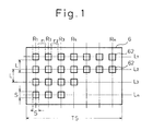
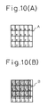
- FIG. 1 An example of the basic configuration of the blanking aperture array 6 used in the present invention is shown in Figure 1.
- a number of blanking apertures 62 are two-dimensionally arranged in order under the conditions as described below.
- Figure 1 (A) is a plan view showing an example of the basic configuration of the blanking aperture array means 6 used in the present invention, and a plurality of blanking apertures 62 of the blanking aperture array means 6 have the same area of aperture and preferably have the almost the same sectional profile.
- the plurality of blanking apertures 62 are arranged in an orthogonal matrix having a plurality of rows and a plurality of stages with equal clearance therebetween both in the vertical and in the horizontal direction.
- the stage (L) direction of the blanking apertures 62 of the blanking aperture array means 6 in the present invention is the direction the charged particle beams are deflected and scanned in the sub field, described later, by the sub deflector 18, that is, a direction that orthogonally intersects the moving direction of the stage 20, and the row (R) direction of the blanking apertures 62 is the direction the charged particle beams are deflected and scanned in the sub field, described later, by the sub deflector 18, that is, a direction that coincides with the moving direction of the stage 20.
- the clearance in the row direction of the blanking apertures 62 in the blanking aperture array means 6 that is, the clearance r1 between the blanking apertures of row R1 and those of row R2, is not specified, it should be set to prevent the charged particle beams that have passed through the blanking apertures 62 from excessively overlapping and result in an excessive proximity effect and deformation of the specified pattern or adjacent patterns from being discontinued when the object to be exposed is exposed to the charged particle beams to form the specified pattern.
- the overall width TS in the row direction of the blanking apertures in the blanking aperture array means 6 is preferably such that the clearance thereof and the number of rows of blanking apertures are set so that the overall width is at least equal to the width ws of the sub field the charged particle beams scan.
- the clearance in the stage direction of the blanking aperture array means 6 in the present embodiment is not limited and is less restricted than the clearance between the rows. It can be determined taking into account the scanning speed of the charged particle beams, the moving speed of the specified pattern in the blanking aperture array means 6, and the moving speed of the stage.
- the overall width TL of the stage direction in the blanking aperture array means 6 is also not limited. As described later, the number of stages is determined depending on the number of times of overlapping irradiation of the charged particle beams onto the specified position of the object,to be exposed, and therefore the overall width TL should be such that it can include at least the number of stages thus determined.
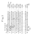
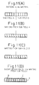
- Figure 2 is a plan view showing the configuration of another embodiment of the blanking aperture array means 6 in accordance with the present invention.
- This embodiment has a configuration in which a plurality of blanking apertures 62 that form one stage L1 and a plurality of blanking apertures 62 that form the other adjacent stage L2 are provided in different arrangement phases in the row direction.
- the blanking apertures 62 forming the first stage L1 and those forming the second stage L2 are provided in a zigzag arrangement.
- each of the blanking apertures 62 has a square cross section, a side of which has the length S.
- aperture stage groups 8 groups, for example, as 1A, 1B; 2A, 2B; ... ; 8A, 8B) each of which (comprising, for example, 1A and 1B) comprises the first aperture stage, for example, 1A (some of the apertures are indicated as 1A 1 , 1A 2 , 1A 3 , 1A 4 , 1A 5 , ...
- 1A n and the number of apertures is, for example, 64) arranged and deviating from one another as much as 2S (50 ⁇ m as an example, 0.1 ⁇ m in terms of dimensional conversion on the specimen) in a direction at right angles to the scanning direction (the vertical direction on the drawing) of the charged particle beams and the second aperture stage, for example, 1B (some of the apertures are indicated as 1B 1 , 1B 2 , 1B 3 , ...
- the number of apertures is, for example, 64 the same as the number of apertures of the first aperture stage), which are arranged while being deviated by the specified distance from the first aperture stage 1A in the scanning direction of the charged particle beams (the vertical direction in the drawing) and by S (25 ⁇ m in the above case, or 0.05 ⁇ m in terms of dimensional conversion on the specimen) from the first aperture stage in a direction at right angles to the scanning direction of the charged particle beams.
- the dimension a shown in Figure 2 (that is, for example, a deviation between the aperture stage 1B and the aperture stage 2B) is 100 ⁇ m (0.2 ⁇ m in terms of dimensional conversion on the object to be exposed), the dimension b is 800 pin (1.6 ⁇ m in terms of dimensional conversion on the object to be exposed) and the dimension c is 3200 ⁇ m (6.4 ⁇ m in terms of dimensional conversion on the object to be exposed).
- the number of apertures of one aperture stage for example, 1A is 64
- the number of apertures of one aperture stage group (for example, comprising 1A and 1B) is 128
- a plurality of blanking aperture stages provided in different arrangement phases are formed as a group and a plurality of groups are repeatedly formed.
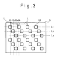
- Figure 3 shows another embodiment of the blanking aperture array means 6 in accordance with the present invention.
- a plurality of types of blanking aperture stages in different phase arrangements are used and the distance between blanking apertures 62 in one aperture stage is as large as an integral multiplication of the example shown in Figure 2.
- the distance L in the row direction of adjacent blanking apertures 62 in one blanking aperture stage is set to be nS or an approximate value nS.
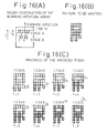
- Figure 16 is a diagram illustrating a configuration of the blanking electrodes in the blanking aperture array means 6 shown in Figures 1 to 3.
- All blanking apertures 62 of the blanking aperture array means 6 are respectively provided with an electrode means 60 that is set to the ON state when the charged particle beams generated by the charged particle beam generating means 1 pass through the blanking apertures 62 and reach the object to be exposed 19 or to the OFF state when the charged particle beams are deflected when passing through the blanking apertures 62 and prevented from reaching the object to be exposed 19.
- the electrode means is adapted to be controlled so that the electrode means is selectively set to the ON state or the OFF state, depending on whether or not the specified voltage is applied by the blanking aperture array control unit 24.
- the electrode means 60 comprises two independent electrode parts 65 and 66 provided near two opposing faces of the blanking aperture and one electrode part 65 is connected to the blanking aperture array control unit 24, and the other electrode part 66 is grounded.
- the control signal line 67 from the blanking aperture array control unit 24 is extended from both ends 70 and 71 in the stage direction of the blanking aperture array means 6 toward the inside of the hollow spaces 73 and 74 formed between the rows of the blanking apertures, and the line 67 is connected to respective electrodes 65 of the blanking apertures.
- the grounding part 68 is provided near the center of the blanking aperture array and the grounding wire 69 is connected from the grounding part 68 to the electrode 66 of each blanking aperture 62.
- variable voltage electrode 65 to be connected to the control means provided on the blanking apertures 62 and the constant voltage electrode 66 to be connected to the constant voltage power supply, such as a grounded power supply
- constant voltage power supply such as a grounded power supply
- a plurality of wires 67 for the variable voltage electrode and a plurality of wires 69 for the constant voltage electrode are arranged from the outer periphery of the blanking aperture array means 6 toward the inside so that they do not intersect each other as shown in Figure 17 (A).
- the distance between adjacent blanking apertures 62 should be increased since the number of lines increases as the number of blanking apertures 62 increases but the size and distance of the blanking apertures cannot be excessively large.
- the charged particle beams are also irradiated to the shift register elements SR and therefore a faulty operation is apt to occur resulting in a defective pattern.
- the method of line connection to the blanking apertures is improved as described below to eliminate the defects of the prior art method.
- the system employs a construction provided with the main line part 68 connected to the constant voltage power supply part in the charged particle beam passing region; a constant voltage applying wire 69 extended and branched to form the main line part 68 to each of surrounding blanking apertures and connected to the constant voltage electrode 66 of the blanking apertures, and the variable voltage applying wire 67 extended from the outer periphery of the charged particle beam passing region of the blanking aperture array means 6 and connected to the variable voltage applying electrode 65 of the blanking apertures 62.
- variable voltage applying electrodes 65 of the opposing electrodes 60 provided on the blanking apertures 62 of the blanking aperture array means 6 in accordance with the present invention are arranged toward the outer periphery of the blanking aperture array means 6, and the constant voltage electrodes 66 are arranged in a direction where the main line part 68 of the blanking apertures is located.
- One constant voltage applying wire 69 which is integrated by using the above described line connection configuration, is branched at a point nearby the blanking apertures 62 and one of the branched lines is connected to one of the electrodes. Therefore, the number of wires passing through the space between the blanking apertures is reduced and the area of the wiring region is also reduced.
- a signal can almost be simultaneously sent to the electrodes 65 and 66 provided on a plurality of blanking apertures 62, and therefore, the electrode is instantaneously selected and the throughput is improved.
- the line connection passage for the constant voltage applying wire 69 and the constant voltage electrode 66 is shortened and an expansion of the wiring region is prevented.
- variable voltage applying wire 67 to be connected to the variable voltage electrodes 65 of the blanking apertures in this embodiment.
- the blanking aperture array means 6 in which there are 16 stages, each of which is formed by a plurality of blanking apertures 62 as shown in Figure 19 where the array of the blanking apertures of odd-numbered stages is deviated by one pitch from the array of the blanking apertures of even-numbered stages in the array configuration, a set of eight variable voltage applying wires 67 are connected toward the inside from the edge part 70 of one blanking aperture array means 6 between the blanking apertures 1A1 and 1A2 of the first stage.
- the wires can be directly connected from the above described edge part to the variable voltage electrodes 65 of the blanking apertures 1A1 and 1A2 and therefore seven wires can be inserted toward the inside between the blanking apertures 1A1 and 1A2.
- Branching and integration of such sets of wires are repeated for the following stages up to the final stage, that is, the eighth stage, while the number of wires is reduced in each stage as described above.
- the wiring is the same as said wiring structure and is executed from the other edge part 71 of the blanking aperture array means 6.
- the number of blanking apertures 62 is increased and the wiring spaces are limited in the array configuration of the blanking apertures as shown in Figure 1, and therefore, the number of blanking apertures 62 is limited.
- substantially large spaces 73 and 74 can be secured among blanking apertures 62 and an increased number of blanking apertures can be sufficiently accommodated.
- half of the total number of wires required for connection are connected in a manner as shown in the drawing from both ends of the blanking aperture array means 6 in the stage direction, that is, the end parts 70 and 71 of the blanking aperture array means 6 as shown in Figure 18, and therefore, the number of wires that are inserted from one end part can be reduced, larger spaces can be reserved and the wiring design will be provided an allowance.
- the electrodes 60 provided at the blanking apertures 62 are turned on or off independently by the beam ON/OFF signal generator 33 of the blanking aperture array control unit 24 and therefore the wiring to the electrodes should be formed independent of other wiring.
- the electrodes 65 are directly connected to the blanking aperture array control units 24, that is, the wiring to the blanking electrodes are shown with dot lines.
- symbol l 1 denotes the wiring to the blanking electrode of the blanking aperture 1A, in the above described aperture stage 1A and similarly, for example, symbols l 2 , l 3 and l 4 are respectively the wiring to the blanking electrodes of the blanking aperture 2A 1 in the aperture stage 2A, the aperture 3A 1 in the aperture stage 3A and the aperture 4A 1 in the aperture row 4A.
- a solid line 68 indicates a common wire 68 for supplying a specified constant voltage, for example, the ground (GND) to the electrodes 66 provided on the other internal surfaces of the blanking apertures 62.
- GND ground
- Figure 18 (A) shows the wiring pattern to the electrodes provided at the apertures that belong to the aperture stages 1A and 4B and Figure 18 (B) shows the wiring pattern to the electrodes provided at the apertures that belong to the aperture stages 5A to 8B. Accordingly, in the actual blanking aperture array means 6, upper portion of Figure 18 (B) connects to the bottom portion of Figure 18 (A) as shown in Figure 19.
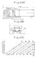
- Figure 4 shows an example of main deflection and sub deflection of the charged particle beams, which are irradiated onto the object to be exposed, by the scanning signals supplied to the main deflector 14 and the sub deflector 18, and the Y direction is the stage moving direction.
- the sub field region SF 1 on the specimen with a width of, for example, 5 ⁇ m in the X direction and a length of, for example, 100 ⁇ m in the Y direction is raster-scanned with line beams within 5 ⁇ sec in the arrow direction in the drawing and subsequently the adjacent sub field region SF 2 is raster-scanned at the same speed as above in the reverse direction (the arrow direction in the drawing).
- the above operation is carried out according to the scanning signal from the sub deflector 18 (sub deflection).
- Figure 4 (B) shows an array of line beams in the sub field (for example, SF 1 ) with a 5 ⁇ m width (one beam size is 0.05 ⁇ m ⁇ and the beam is circular on the surface) and symbol A 1 denotes the beam that passes through an aperture of the first aperture stage (for example, 1A) and symbol A 2 is the beam that passes through an aperture of the second aperture stage (for example, 1B).
- the sub field region with 5 a ⁇ m width is scanned with 100 line beams A 1 , A 2 , ... A100.
- the total sum of the apertures of the first aperture stage (for example, 1A) and those of the second aperture stage (for example, 1B) is 128 in the above sample. Accordingly, each 14 line beams A11 to A14 and A 1R to A 14R are arrayed beyond the right and left boundaries of the sub field region (for example, SF 1 ). Accordingly, the length of 128 line beams is 6.4 ⁇ m.
- Figure 4 (C) is a diagram showing the scanning waveforms in the Y direction of the above sub deflection; the horizontal axis denotes the time elapsed, and the vertical axis denotes the positions of beams in the Y direction on the surface of the object to be exposed.
- 1de notes the position of the beam that has passed through the aperture stage 1B; 2denotes the position of the beam that has passed through the aperture stage 1B; 3denotes the position of the beam that has passed through the aperture stage 2A, and the following numbers similarly denote the positions of the beams that have passed through the aperture stages.
- the charged particle beams that have passed through the aperture stages move as far as 0.05 ⁇ m on the surface of the object to be exposed every 2.5 nsec and, after the lapse of 5 nsec, the charged particle beams that have passed through the following aperture stages come up to the same position on the surface of the object to be exposed.
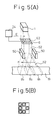
- FIG. 5 (A) briefly shows the principal part of the charged particle beam exposure system in accordance with the present invention.
- Charged particle beams 52 emitted from the electron gun 1 pass through the groups of blanking apertures 62 of the blanking aperture array means 6 and are scanned by the electromagnetic deflection means 50 on the object to be exposed in the direction of arrow F.
- the blanking aperture array means 6 a plurality of blanking apertures 62 are arranged in two dimensions as described above and individually ON/OFF controlled by the blanking aperture array control means 24.
- the specified pattern 55 is formed on the blanking aperture array means with the blanking apertures 62 which remain in the ON state according to the above described control and moved in the direction of arrow E according to the control of the blanking aperture array control means 24.
- the electromagnetic deflection means 50 operates to deflect and irradiate the charged particle beams 52 onto the position B1 near the end part of the sub field 19s on the object to be exposed 19.
- the electromagnetic deflection means 50 moves the charged particle beams 52 slightly to the left to the position B2 from the irradiating position B1 in the preceding process and the irradiation is executed at this position.
- the charged particle beams 52 that have passed through the blanking apertures (L2, R2) irradiate again the position P1 of the object to be exposed 19 onto which the charged particle beams are irradiated in the first process and two charged particle beams 52 that have passed through the blanking apertures (L1, R1) and (L1, R3) irradiate positions P2 and P3 of the object to be exposed 19.
- the scanning direction and speed of the charged particle beams 52 and the moving direction and speed of the pattern in the blanking aperture array means 6 are adjusted taking into account the conditions such as the shape of the pattern, the distance between adjacent blanking apertures, etc. to operate all means at the specified timing and exposure by turning on the specified blanking apertures 62 of the blanking aperture array means when the charged particle beams reach a position to be irradiated of the object to be exposed.
- control allows the irradiation of the charged particle beams 52 repeatedly at the same position of the object to be exposed 19.
- the specific position P1 of the object to be exposed 19 is irradiated two times with the charged particle beams, in this step.
- the specific position P1 of the object to be exposed 19 is to be irradiated with the charged particle beams that have passed through blanking apertures different from the blanking apertures (L1, R2) and (L2, R2) in the blanking aperture array means 6.
- the electromagnetic means 50 moves the charged particle beams 52 slightly leftward from the irradiating position B2 in the preceding process to the position B3, whereby the irradiation is executed.
- the charged particle beams 52 that have passed through the blanking apertures (L3, R3) are irradiated again onto the position P1 of the object to be exposed 19; the position of which the charged particle beams were irradiated in the second process.
- Two charged particle beams 52 that have passed through the blanking apertures (L2, R1) and (L2, R3) are irradiated again onto positions P2 and P3 of the object to be exposed 19; the position of which the charged particle beams were irradiated in the second process, and three charged particle beams 52 that have passed the blanking apertures (L1, R1), (L1, R2) and (L1, R3) are irradiated onto positions P4 to P6 of the object to be exposed 19.
- the specific position P1 of the object to be exposed 19 has received irradiation of charged particle beams three times and the specific positions P2 and P3 have received irradiation of charged particle beams two times in this step.
- Any type of pattern can be easily exposed by repeating such processes and all pixels of the pattern are exposed by a plurality of irradiations of the charged particle beams. Depending on the case, all pixels of the pattern need not be irradiated the same number of times and the number of irradiation times with charged particle beams for part of the pixels can be reduced.
- a single straight line type pattern can be formed by exposing the clearance portion of a straight intermittently exposed part formed on the object to be exposed 19 by the blanking apertures 1A 1 , 1A 2 , 1A 3 ... of the stage 1B to the charged particle beams formed through the blanking apertures 1B 1 , 1B 2 , 1B 3 ... of the stage 1B.
- the exposure can be executed by operating the control means so that the irradiation is carried out when the charged particle beams that are formed by the blanking apertures 1B 1 , 1B 2 , 1B 3 ... of the aperture stage 1B reach the clearance portion of a straight intermittently exposed part formed on the object to be exposed 19 by the blanking apertures 1A 1 , 1A 2 , 1A 3 ... of the aperture stage 1A.
- the specified position of the object to be exposed 19 is exposed and irradiated a plurality of times by the charged particle beams that have passed through different blanking apertures. Strictly speaking, the same position is rarely irradiated precisely a plurality of times and a slight deviation of the irradiating position of the charged particle beams is unavoidable.
- a region including a certain allowance around the predetermined position on the object to be exposed as the center is irradiated by a plurality of charged particle beams.
- the above embodiment is described as an example where the stage 20, on which the object to be exposed 19 is mounted, is not moved when the charged particle beams are irradiated for exposure, that is, as the step and repeat system.
- a continuous moving system by which the scanning of the charged particle beams and the stage at the same time can be performed. In this case, a complex control system is required.
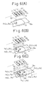
- Fig. 16 shows a process of exposure of a predetermined pattern using the blanking aperture array in another embodiment of the present invention.
- the process is illustrated in Fig. 16 (C) to draw the pattern as shown in Fig. 16 (B) only by the charged particle beam passing through one group of apertures constituted by the first aperture row (as row A, and including three apertures 1, 3 and 5) and the second aperture row (as row B, and including two apertures 2 and 4).
- the respective apertures 1, 3 and 5 of the first aperture row offset the above-mentioned pitch 2S in a direction perpendicular to the scanning direction
- the respective apertures 2 and 4 of the second aperture row are offset relative to respective apertures 1, 2 and 3 of the first aperture row in a magnitude of pitch S.
- Fig. 16 (C) shows shifting of the reference line shown as Line Y0 in Fig. 16 (A) on the sample according to a shifting of the position of the raster scan.
- a plurality of groups (8 groups in the foregoing example) of apertures are aligned in the scanning direction of the charged particle beam (namely, arranging the blanking aperture groups in several rows, e.g., 8 columns in scanning direction, in the scanning-direction), so that the same exposure of the same region on the object to be exposed within the same scanning timing with a timing delay. Namely, in the above-mentioned example, exposure is performed 8 times.
- This can be easily done by an analog current driving type amplifier.
- Fig. 8 shows a rising waveform of an output current (the output current of the above-mentioned analog current driving type amplifier) supplied to the re-focusing coil when exposure of the charged particle beam employs the braking aperture arrangement of the present invention, and in which is illustrated a variation from the minimum value to the maximum value over 80 nsec.
- the vertical axis indicates the number of aperture columns through which the beam of raster scan passes, and in the shown example, sixteen aperture columns of 1A to 8B are provided.
- the number of beams in ON state is increased so that even when the value of the beam current becomes large, the charged particle beam 8 can be accurately focused on the surface of the sample 19 by supplying the predetermined re-focusing current to the re-focusing coil, as shown in Fig. 7 (C).
- the deflecting position error (the error in the lateral direction as shown by broken line in Fig. 7 (C) can be compensated by supplying the deflection signal proportional to the number of beams in an ON state for the sub-deflector 18 via a re-focusing flyback 35.
- the exposure amount can be reduced for 1/8 of the necessary exposure amount for reducing one beam shot. This can be advantageously applied to the applications shown in Figs. 9 to 11.
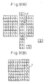
- Fig. 9 (A) shows one example for the correction of proximity effect (phenomenon causing fogging of the energy in the region adjacent to the region having a high exposure amount due to reflection of the irradiated charged particle beam from the inside of the substrate to the resist).
- the figures shown in respective irradiating regions represents the number of shots of the charged particle beam (same in Figs. 9 through 11).
- Fig. 9 (A) by reducing the overall exposure amount for the large pattern, even when the patterns A and B are located close to each other, no fogging of the irradiated energy occurs in the intermediate region C. Therefore, adjoining of the patterns A and B via the intermediate region C can be eliminated.
- Fig. 9 (B) shows another example of a correction of the proximity effect by the exposure method according to the present invention. As shown, by reducing the exposure amount of the large pattern A other than the circumferential region thereof, the affect of the proximity effect can be reduced to make the outline of the pattern clear.
- Fig. 10 shows an example, in which the exposure pattern shifts at a magnitude smaller than the beam size.
- Fig. 11 shows an example of exposure for the joint between fields or sub-fields employing the exposure method according to the present invention. It is assumed that the desired exposure pattern extends from A sub-field to B sub-field across the border therebetween, as shown in Fig. 11 (A).
- Fig. 11 (D) shows the exposure pattern when the image from respective sub-fields are slightly offset from each other. It is assumed that A represents the drawing pattern from the A sub-field and B represents the drawing pattern from the B sub-field. The drawing pattern formed by combining these two patterns is represented by C. By this, the pattern that is substantially continuous at the joint in comparison with that drawn independently from respective sub-fields, can be drawn. As set forth above, by lowering the exposure amount at the border region of the fields or sub-fields and by performing an exposure in an overlapping manner for the fields or sub-fields so that the same positions can be exposed from respective adjacent fields or sub-fields, the joint between adjacent fields or sub-fields can be smoothly connected.
- the following table 1 shows practical values of various data when exposure of the charged particle beam is performed employing the method according to the present invention.
- the beam size at the surface of the sample is set to be 0.05 ⁇ m ⁇ .
- the current density is set to be 250 A/cm 2 .
- the current value of a single beam becomes 6.26 nA.
- the stage shifting speed is set to be 50 mm/sec in Y direction.
- the main deflection is 2 mm/2 msec in X direction and the sub deflection is 5 ⁇ m ⁇ 100 ⁇ m/5 ⁇ sec in Y direction.
- the re-focus time (allowed period for increasing the re-focusing current from the minimum value to the maximum value) is 80 nsec, as set forth above.
- the present invention even when the number of charged particle beams is increased, re-focusing for compensating focus error due to Coulomb interaction can be facilitated to allow the formation of a sharp pattern. Also, even when a plurality of aperture groups are formed, the wiring for respective electrodes on the blanking aperture array becomes easy. Furthermore, the present invention allows a substantially high density exposure with no gaps between irradiated points.
- the basic method thereof is completely different from that of USP 4153843 in that the exposure operation is carried out in such a way that the charged particle electron beams expose all of the predetermined exposure region simultaneously therein by utilizing a blanking aperture array in which all of the apertures are arranged two dimensional and all of the apertures formed in the aperture array are used simultaneously.
- an inner diameter of the blanking aperture and a pitch thereof can be set previously at a suitable dimension respectively, so that all of the exposed positions formed on the sample to be exposed are in contact with each other and thus a plurality of the beams can be controlled easily without creating defecting portions-as shown in the conventional technology.
- both the aberration and the reduction ratio of all the beams can be controlled at the same level.
- the charged particle electron beams are simultaneously exposed on the plurality of addressed positions adjacently arranged on the sample to be exposed, all of the addressed positions formed on the sample can be exposed with approximately the same conditions when the addressed positions are exposed with the beam each having the same intensity.
Abstract
Description
- The present invention relates to a charged particle beam exposure system that is adapted to continuously scan a number of charged particle beams with a blanking aperture array having a number of rows of open holes.
- Lately, because of their increasing importance ICs have been expected to advance in terms of integration density and function as core technology for technological progress of industrial fields including computers, mechanical control, communications, etc. ICs have reached a four-fold level of high integration within the last three or four years. For example, the integration density of the DRAM has increased from 1M through to 4M, 16M, 64M, 256M and 1G.
- Said high integration development has depended solely on the advancement of precision fabrication technology, particularly the advancement of optical technology that allows precision operations in 0.5 µm units. However, the precision limit of optical technology is approximately 0.3 µm and it is becoming difficult to maintain a precision of 0.10 µm in windowing for contact holes and alignment with a pattern of a lower layer. Since a pellicle cannot be applied to a mask in the case of X-ray exposure and a defect-free guarantee is difficult, X-ray exposure cannot be used in the fabrication of LSIs that are required to provide high reliability.
- Though, in charged particle beam exposure, precision operations of 0.10 µm or under can be achieved with alignment accuracy of 0.05 µm, and it has been considered that charged particle beam exposure could not be used for volume production of LSIs because of low throughput. In this case, a one-line configurated pattern exposure system has been assumed for precision pattern exposure with at most only one Gaussian beam or variable square beam. The above assumption has been determined in view of the productivity of the existing commercial systems, not based on the results of checking physical and technological bottlenecks and clarification of causes as to why the said throughput could not be increased or consideration as to how the throughput could be increased.
- Lately, however, the inventions of a block exposure system and a blanking aperture array system by the inventor of the present invention and others have made it possible to expect a throughput of approximately 1 cm2/sec. This exposure system is so advantageous that other lithographic means cannot compare in terms of precision, alignment accuracy, quick turnaround, reliability and advancement of softwares. The charged particle beam exposure system that enables the manufacturing of nano-lithographic LSIs such as 1 to 4 GBIT memories, is considered prospective lithography system.
- The most popular type of charged particle beam exposure system is the point beam raster scan exposure system. However, in this system, only one beam is used and the throughput is extremely low and therefore the exposure of wafers is impossible in the volume production level.
- On the contrary, in the case of the variable square beam system, a limited size of square can be formed by one shot and therefore a satisfactory throughput can be obtained with a rough pattern; the smallest pattern of which is approximately 2 µm. Accordingly, this system can be used for direct exposure production of small lots of products. However, LSIs of high pattern density cannot overcome the restriction of a one-writing pattern and cannot avoid an extremely low throughput.
- As a supplementary system for the above, a system for transferring a repetitive memory pattern as a contraction image of charged particle beams passing through a silicon stencil mask is referred to as the block exposure system. This block exposure system allows volume production of memory chips of 256M and 1G by repeatedly irradiating a pattern, which is often used for the memory at a high repetition rate.
- However, the block exposure system has the vital defect that the throughput for a random pattern is extremely low as in case of the variable square beam. Most gate arrays and micro computers are often based on random patterns.
- As a method for high speed exposure of such random patterns, a method has been proposed using line beams with the blanking aperture array. Figure 14 shows an example of a configuration of the prior art blanking aperture array, and this
blanking aperture array 6 is provided with a row ofopenings 62 that are a plural number of apertures arranged in a line. An ON or OFF signal from the beam ON/OFF signal generator 33 is entered independently into theelectrode 61 provided at an inside surface of each opening 62 through circuit lines ℓ1, ℓ2, ... ℓn and a constant voltage (for example, a ground potential) is applied to theelectrode 63 provided at the other inside surface of opening 62 through a common line. - Thus, a plurality of beams passing through the
openings 62 are arranged in a line and theseblanking apertures 62 are ON/OFF controlled by an appropriate control means. - In other words, the system is adapted so that the charged particle beams that have passed through the
blanking apertures 62, into which the ON signal is entered, reach the specified point on the surface of object to be exposed and the specified point is exposed and the charged particle beams that have passed through theblanking apertures 62 into which the OFF signal is entered, is interrupted by an appropriate shield plate and prevented from reaching the surface of object to be exposed. Then a specified pattern is exposed as if it is scraped with a brush while scanning a plurality of charged particle beams obtained by the above described ON/OFF control. - For volume production by direct exposure of wafers, it is necessary to expose a 1 cm2 segment of wafer within one or, at longest, two seconds. If the throughput is determined as described above, the second problem is a sensitivity of resists. Electrons are particles and the number of electrons that are incident into a unit area within a unit time varies in terms of the Poisson's distribution and therefore the resolution is basically in inverse proportion to a square root of the sensitivity. Accordingly, if the smallest pattern is 0.2 µm, a resist with the sensitivity of 5 - 10 µC/cm2 is generally required. A high sensitivity resist has only a low resolution and the system for which implementation of high sensitivity is excessively expected cannot be used in actual volume production of LSIs.
- If the throughput of 1 cm2/sec is a target value for the resist sensitivity of 5 - 10 µC/cm2, the required overall current is 5 - 10 µA. Another beam size is assumed as 0.05 µm□ on the surface of a specimen. The limit of the thermal electron gun of LaB6 is a current density of 250 A/cm2 to be obtained using a lens of an extremely small spherical aberration and chromatic aberration factor. Accordingly, the current density of 0.05 µm□ is 250 A/cm2 and therefore the current value of one beam is 250 x (0.05 x 10⁻⁴)2 = 6.25 nA. The overall current value of 1600 beams is 10 µA.
- The problems in the case of exposure of the specified pattern with the above described line beams (for example, 1600 line beams) using the blanking aperture array as shown in Figure 14 are as follows:
- (1) A coulombic interaction has been considered a physical bottleneck for the charged particle beams. This coulombic interaction is a phenomenon such that the beams become dim because of interactive repulsion of electrons. The main cause of this phenomenon is that the focal distance is extended because of interactive repulsion of charged particle beams in proportion to the current value of overall electron flow in the lens near the surface of specimen (in other words, in proportion to the number of charged particle beams in the ON state) and the focal point deviates downward from the specimen surface (that is, the surface of wafer 19) as shown in Figure 7 (B).
- In Figure 7 (B),
numeral 8 denotes the charged particle beam in the ON state andnumerals charged particle beams 8 in the ON state is small as shown in Figure 7 (A) but occurs when the number ofcharged particle beams 8 in the ON state is large (the maximum number of beams reaches, for example, 1600 as described above) as shown in Figure 7 (B). - The focal deviation because of said coulombic interaction can be corrected by providing a small refocus coil (for example, approximately 4 mm in diameter) at a position near the peak of the magnetic field in the final stage lens or the preceding lens (that is, a position where the magnetic field is most intensified) and supplying a refocus current in proportion to the current value of all charged particle beams (that is, the number of charged particle beams that remain in the ON state at that time) to the refocus coil at the rate of, for example, 50 nsec (50 + 1 sec). In this case, the rate of approximately 50 nsec is the limit of the response speed of the amplifier (analog current-driven type amplifier) for supplying the specified refocus current to the refocus coil in accordance with the number of charged particle beams that remain in the ON state at that time.
- If the size of one beam is set to 0.05 µm□ and the scanning speed is set to 100 µm/5 µsec (that is, 0.05 µm/2.5 nsec) in the stage moving direction by using the line beams through the blanking aperture array as described above, the beam dwell time per 0.05 µm (one shot of irradiation beam) is 2.5 nsec. Since such line beams are scanned at a high speed, it is necessary to vary the refocus current (for example, approximately 1A, maximum) in steps (for example, 0A to 1A) within a time far shorter than 2.5 nsec, which is the beam dwell time at the above-described point at the boundary between the exposure of a completely written-out region and the partially exposed region. However, it is impossible to obtain said response speed even with the advancement of analog current-driven type amplifiers, which have been developed recently. Accordingly, as shown in, for example, Figure 15, if there is a pattern as a small projection (in other words, when the pattern B is exposed, only two beams of the line beams become ON as shown with
black dots black dots - (2) Since the beam dwell time of 20 nsec is required for the resist sensitivity of 5 µC/cm2 , a current density of 250 A/cm2 is insufficient in the beam dwell time of 2.5 nsec described above. A current density of 2000 A/ cm2 is required to obtain the dwell time of 2.5 nsec and therefore general thermal electron guns and electron lenses cannot attain this level of current density.
- (3) An intermediate color cannot be represented with the conventional line beams and a pattern of dimensions as large as an integral multiple of the dimensions of a single beam cannot be formed. Though such pattern can be formed by plural times of movement of the stage or beam scanning, the throughput is extremely low and volume production cannot be carried out.
- (4) The amount of exposure with the conventional line beams cannot be reduced by a proximity effect correction.
- (5) If the conventional line beams are arranged to reduce the effect of the electric field of the openings adjacent to the blanking aperture array, the irradiation points become vacant and therefore the scanning of a plurality of line beams that are slightly deviated is repeated and the throughput will be reduced.
- In other words, the problems associated with a blanking aperture array that comprises the above described plurality of blanking
apertures 62 arranged in a row can be summarized as described below. - The exposure efficiency with the charged particle beams can be improved by using said blanking aperture array, whereas a resist that provides a higher resolution should be used in accordance with the degree of precision of a pattern to be exposed and therefore the exposure time becomes longer and the throughput is reduced.
- In said blanking aperture system, there is a problem that the lens system is affected by the total amount of charged particle beams that pass through the above described blanking apertures, the focal point deviates and the pattern is dimmed. When exposing, for example, a pattern as shown in Figure 15, there is a problem that the total amount of charged particle beams passing through the blanking aperture array substantially varies in the exposure of the B row pattern after exposure of the A row pattern; the focal distance of the charged particle beam exposure system deviates significantly and therefore a considerably large current is required and it takes a certain period of time for correction.
- For this reason, it is necessary to provide a special control adjustment circuit.
- In addition, in said blanking aperture system, the exposure should be carried out through the blanking apertures that are arranged as close to each other as possible to prevent such defects as deformation or discontinuity of the pattern or the like. However, the charged particle beams have a fixed intensity distribution as described above and therefore there is the so-called proximity effect that adjacent charged particle beams interfere with each other and the pattern is exposed beyond the predetermined amount of irradiation. For example, it is necessary to adjust the amount of irradiation of the charged particle beams at the center and both ends of the blanking aperture array. However, such adjustment has been difficult in the conventional blanking aperture array.
- In some cases, it is necessary to vary the amount of irradiation on part or all of the pattern, depending on the shape of the pattern or the relative position of the pattern to other patterns but such variation cannot be implemented by the conventional blanking aperture array.
- Some examples of two-dimensional arrangement of the groups of blanking apertures in the above described blanking aperture array unit have been known to solve the above problems. In the blanking aperture array unit provided with the blanking apertures that are two-dimensionally arranged as described above, all charged particle beams forming the specified pattern passing through the blanking aperture array unit are simultaneously irradiated onto the specified position of an object to be exposed to carry out an exposure process and subsequently all charged particle beams formed in the same or different pattern are simultaneously irradiated onto an adjacent object to be exposed to carry out the exposure processing. If the total amount of charged particle beams passing through the blanking apertures of the above described blanking aperture array unit largely differs with each pattern, a refocusing problem as described above occurs and the proximity effect problem is not resolved and there is no possibility of varying the amount of irradiation onto part of the specified pattern.
- And further, a high speed pattern forming method is disclosed by USP 4153843 in which a blanking aperture array provided with a plurality of blanking apertures arranged in two dimensional form is used and thus a plurality of charged particle electron beams are radiated on a surface of a sample to be exposed to the beam to form a predetermined pattern thereon and wherein a total amount of radiation value at a certain addressed position of the sample to which,a respective charged particle electron beam is to be exposed.
- In the method disclosed in the USP 4153843, as shown in Fig. 20, each one of the charged particle electron beams formed by each one of the apertures A, B, and C forming a first aperture line arranged parallel to a scanning direction Y of the charged particle electron beams radiates each one of addressed positions of the sample forming one
line 1 arranged parallel to the scanning direction Y of the charged particle electron beams and each one of the charged particle electron beams formed by each one of the apertures B, E, and H forming a second aperture line arranged parallel to a scanning direction Y thereof, radiates each one of addressed positions of the sample forming anotherline 6 arranged parallel to the scanning direction Y and while each one of the charged particle electron beams formed by each one of the apertures C, F, and I forming a third aperture line arranged parallel to a scanning direction Y thereof, radiates each one of addressed positions of the sample forming anotherline 11 arranged parallel to the scanning direction Y. - Note, that the charged particle electron beams formed by apertures forming respective lines radiate addressed positions formed on any one of the lines on the sample, and each line is separated a predetermined space from each other.
- Accordingly, the spaced addressed positions are successively radiated by each one of the charged particle electron beams formed by each one of the aperture lines formed in the aperture array and thereby all addressed positions are ultimately fully exposed; this method is generally called an interleave method.
- And thus, the charged particle electron beams formed by the aperture A exposes sequentially continuously arranged addressed positions to form in turn a line on the samples, (1, a), (1, b), (1, c) ... (1, 1), (2, 1), (2, k), ... (2, a), (3, a), (3, b), ... (3, 1).
- On the other hand, the charged particle electron beams formed by the aperture B exposes sequentially continuously arranged addressed positions to form in turn a line on the samples, (6, a), (6, b), (6, c) ... (6, 1), (7, 1), (7, k), ... (7, a), (8, a), (8, b), ... (8, 1).
- Further, the charged particle electron beams formed by the aperture C exposes sequentially continuously arranged addressed positions to form in turn a line on the samples (11, a), (11, b), (11, c) ... (11, 1), (12, 1), (12, k), ... (12, a), (13, a), (13, b), ... (13, 1).
- The characteristic feature of the conventional technology is such that a plurality of addressed positions formed on the sample, each of them being separated a predetermined distance from each other, are simultaneously and respectively exposed to different charged particle electron beams in a predetermined exposed region.
- In the conventional technology, the charged particle electron beams formed by the apertures D and G in the first apertures line formed by the apertures A, D, and G expose the same addressed position to which the charged particle electron beam formed by the aperture A exposes successively with a predetermined time difference. Therefore, in the embodiment as shown in Fig. 20, one of the addressed positions in the sample to be exposed will be exposed three times by the charged particle electron beam and therefore, a dose value of the same addressed position caused by the exposure of the beams can be optionally changed by changing the exposure number within 3 times. The conventional technology, however, discloses that each of the charged particle electron beams exposes each one of the addressed positions respectively and thus control of the beam is difficult.
- Therefore, a problem arises in that-when the beam exposes all of a predetermined region to be exposed, a disconnected portion among the pattern to be formed, and which should naturally be connected, will appear because of a displacement of the beam from an addressed position to be correctly exposed.
- Accordingly, in the conventional technology, since the charged particle electron beams expose addressed positions separated from each other, an aberration and a reduction ratio of each one of the charged particle electron beams changes because of the difference in the distance from the optical axis and thus another technology is required to adjust the displacement. And further, in the conventional technology, since the controlling operation for controlling the deflection of the beam to realize the interleave operation becomes difficult the beam controlling circuit becomes complicated.
- Moreover, in the conventional technology, a predetermined time should be required from the time when the beams have exposed one addressed position to the time when the same beams expose another adjacent addressed position.
- Generally, a light sensitive layer formed at a predetermined addressed position is affected by another beam that exposes another addressed position next to the predetermined addressed position, and thus in the conventional technology, since the exposure time is different, the exposed condition of the sensitive layer of one addressed position will change as time elapses.
- Accordingly, it becomes difficult to maintain the light sensitive condition of the predetermined addressed position at the predetermined level and a uniform exposure operation cannot be expected.
- An object of the present invention is to provide a means for solving the various above described problems in the exposure method by the conventional line beams, particularly a charged particle beam exposure system capable of easily correcting the focal deviation of charged particle beams due to the above described coulombic interaction to allow the formation of a sharp pattern when any type of exposure pattern is used and the number of charged particle beams is increased and appropriately varies the amount of irradiation of charged particle beams for each pattern; thereby the proximity effect can be prevented and a pattern having a desired exposure condition can be efficiently formed. In addition, the primary object of the present invention is to obtain a charged particle beam exposure system in which line connections to the electrodes on the blanking aperture array are easy.
- The present invention for solving the above described problems is to provide a method for exposing a charged particle beam and a charged particle beam exposure system of a configuration as described below.
- Specifically a method for exposing a charged particle beam to an object to be exposed with a charged particle beam exposure system comprising, a charged particle beam generating means for generating a charged particle beam, a blanking aperture array means for shaping said charged particle beam generated by said charged particle beam generating means and having a plurality of blanking apertures arranged in two dimensional form, a stage means for holding an object to be exposed, a deflection means for deflecting the charged particle beam passing through said blanking aperture array means by a specified amount in order to irradiate the charged particle beams onto a specified position of said object to be exposed, wherein said method comprising the steps of, a first step of irradiating a pattern formed by said charged particle beams arranged in two dimensional configuration on a first region specified on said object to be exposed, a second step of successively irradiating the pattern formed by said charged particle beams arranged in two dimensional configuration on a second region having an overlapping region in which at least a portion of said second region and at least a portion said first region overlap each other on said object to be exposed, and wherein when said charged particle beams are irradiated on said object to be exposed, first charged particle beams passing through a first blanking aperture irradiates a specified first region on said object to be exposed in said first and in said second steps, second charged particle beams passing through a second blanking aperture arranged next to said first blanking aperture overlaps and irradiates a region closely arranged to said first region so that said specified position in said overlapping region is overlapped and irradiated a plurality of times by respective charged particle beams each having a certain irradiation amount set by dividing a total irradiation amount of said position on said object to be exposed by a predetermined number of radiating steps.
- In other words, in a method for exposing the charged particle beam in accordance with the present invention, a group of charged particle beams having a specified pattern that have passed a plurality of blanking apertures two-dimensionally arranged are not simultaneously irradiated onto the specified position of the object to be exposed unlike the prior art system and part of the specified pattern to which the specified position of the object is exposed is divided and irradiated a plurality of times. In addition, the charged particle beams to be irradiated onto the specified position of the object to be exposed are supplied through different blanking apertures, respectively.
- Accordingly, the unit exposure points that form a pattern on the object to be exposed overlap and are irradiated as many times as specified with the above described plurality of charged particle beams.
- More specifically, for example, the blanking aperture array control unit is constructed so that the same pattern as the specified pattern to be exposed to the charged particle beams or the same pattern as at least part of the specified pattern is formed with the groups of blanking apertures that remain in the ON state at a specified region of the object to be exposed and the specified pattern is moved on the blanking aperture array in the specified direction while synchronized with the deflection scanning of the charged particle beams.
- Movement of the pattern on the blanking aperture array and deflection scanning of the charged particle beams by means of electromagnetic deflection are controlled by an appropriate control means so that the charged particle beams are irradiated onto the same position of the object to be exposed even when the charged particle beams forming part of a special pattern by exposure pass through different apertures of the blanking apertures on which the pattern moves.
- In other words, the construction is such that the specified region of the object to be exposed is exposed, in a specified pattern, to the charged particle beams passing through the specified blanking apertures of the blanking aperture array that remain in the ON state when the charged particle beams are scanned by the electromagnetic deflection means, and the specified position and the ambient part of the object to be exposed overlap and are irradiated in sequence with a plurality of charged particle beams that have passed through different blanking apertures at a specified time interval when the blanking aperture array control unit controls the movement of the specified pattern, which is formed on the blanking aperture array, in one direction.
- According to the above described construction, the amount of irradiation necessary for the resist provided on the object to be exposed to completely form a pattern is divided a plurality of times (n times) when forming the specified pattern to be formed on the object to be exposed, and therefore the intensity of the charged particle beams irradiated at one time is 1/n of the amount of irradiation generally required for forming the pattern. Even though the pattern to be exposed is suddenly changed, the electron density of each charged particle beam is extremely small and therefore the above described refocus problem will not occur and the refocusing operation is easily carried out in a short period of time since the focal deviation is slight even though such deviation occurs.
- In addition, in the present invention, the charged particle beams are scanned and irradiated in sequence in, for example; the stage direction of the groups of blanking apertures provided on the blanking aperture array, and therefore the variation of electrons due to the groups of charged particle beams that change at a time, is far smaller than the whole blanking aperture array and there is no possibility of the refocus problem occurring.
- In the present invention, the charged particle beams for forming a specific part of the specified pattern pass through the blanking apertures, which are individually controlled and, at the same time, the charged particle beams supplied from different blanking apertures overlap and are irradiated in sequence onto the same position of the object to be exposed at a specified time interval. Depending on the case, the number of overlapping irradiation can be freely changed by changing over the ON state of the specified blanking apertures to the OFF state to reduce the number of times of irradiating operations and the disadvantages associated with the prior art can be eliminated.
- In the present invention, the speed of an irradiating operation is substantially increased since the intensity of charged particle beams required to form each pattern can be reduced and,the construction of the apparatus can be small since the configuration of the control stages can be simplified.
- In addition, since the groups of blanking apertures provided on the blanking aperture array are arranged in a checkered pattern so that, for example, the first aperture stage and the second aperture stage do not contact each other and therefore, even when there are many groups of apertures, line connection to the electrodes provided on the blanking apertures is easy and the specified pattern of the object to be exposed can be exposed without clearance and in a coordinate direction orthogonally intersecting the scanning direction with the charged particle beams passing through the first row of openings and the charged particle beams passing through the second row of openings of the groups of blanking apertures.
- Figure 1 is a diagram showing the basic configuration of the blanking aperture array used in the present invention.
- Figure 2 is a diagram showing another configuration of the blanking aperture array used in the present invention.
- Figure 3 is a diagram showing a further another configuration of the blanking aperture array used in the present invention.
- Figures 4 (A) and 4 (B) are respectively a diagram showing the relationship between an example of main deflection and sub-deflection of the charged particle beams and the direction of the blanking aperture stage of the blanking aperture array means in accordance with the present invention and Figure 4 (C) is a diagram showing the scanning waveforms of charged particle beams in the sub-deflection direction (Y direction).
- Figure 5 is a diagram illustrating the principle of the exposure method in the charged particle beam exposure system in accordance with the present invention.
- Figure 6 is a diagram illustrating the principle of the exposure method in the charged particle beam exposure system in accordance with the present invention.
- Figure 7 is a diagram illustrating the function of the refocus.
- Figure 8 is a diagram illustrating the output current waveforms supplied to the refocus coil.
- Figure 9 is a diagram showing an example of a proximity effect correction by the exposure method in accordance with the present invention.
- Figure 10 is an explanatory diagram for forming an exposure pattern shifted by a smaller size than the beam size according to the exposure method of the present invention.
- Figure 11 is an explanatory diagram for exposing the stitch of the fields or the, sub-fields by the exposure method of the present invention.
- Figure 12 is a diagram showing an example of the overall configuration of the charged particle beam exposure system in which the method in accordance with the present invention is to be embodied.
- Figure 13 is a circuit connection diagram of the electrical system to be connected to the sections of the apparatus shown in Figure 12.
- Figure 14 is a diagram showing an example of the configuration of the prior art blanking aperture array.
- Figure 15 is a diagram describing an exposure problem using the prior art blanking aperture array.
- Figure 16 is a diagram illustrating a practical example of another exposure method for the charged particle beam exposure system in accordance with the present invention.
- Figure 17 is a diagram illustrating an example of line connections of the prior art blanking aperture array.
- Figure 18 is a diagram illustrating an example of line connection-pattern to the blanking electrodes in the blanking aperture array shown in Figure 1.
- Figure 19 is a diagram showing an example of connection of the constant voltage applying circuit to the blanking electrodes in the blanking aperture array shown in Figure 1.
- Figure 20 shows a conventional exposure method.
- The following describes a practical example of the charged particle beam exposure system in accordance with the present invention.
- Figure 12 is a diagram that exemplifies the overall configuration of the charged particle exposure system related to the present invention. In Figure 12, the
electron gun 1 comprises acathode 2 composed of LaB6 and others, agrid 3 and ananode 4.Numerals aperture array 6 construction as described later is provided in theelectron lens 7.Numeral 8 denotes the so-called ON beam, which passes through the blanking aperture to the electrode of which an ON signal is applied among the blanking apertures provided in the blankingaperture array 6 and is irradiated onto the specified point on the object (wafer surface) 19 to be exposed.Numeral 9 denotes the so-called OFF beam, which passes through the blanking aperture to the electrode of which an OFF signal is applied among the blanking apertures provided in the blankingaperture array 6 and is interrupted by an appropriate shielding means, for example, theshield plate 11 provided below the blanking aperture array and is not irradiated onto the surface of the object to be exposed. The above describedrefocus coil 13, which converges the charged particle beams to a specified size onto a specified position, is provided in theelectron lens 12 immediately preceding the final stage in the lens system for focusing on the surface of the object to be exposed. -
Numerals 14 denote the main deflector (which is generally formed with a coil) andnumerals 18 denote the sub deflector (which is generally formed with a static electrode); the charged particle beams (ON beams) 8 are deflected in a specified direction for main deflection and sub deflection, and are described in the following.Numerals 15 denote the dynamic focus, which corrects the position of the focal point in accordance with the deflecting position of the charged particle beams. In addition,numerals 16 denote the dynamic stig, which corrects the shape of charged particle beams irradiated onto the specimen (for example, correction for rounding the shape of the charged particle beams). -
Numerals 20 denote the stage for supporting the object to be exposed 19 and the movement of this stage is detected by thelaser interferometer 22, and the detection signal of the laser interferometer is supplied to thescanning signal generator 32, described later. Specifically, thelaser interferometer 22 reads the position of thestage 20 and feeds back its reading to the scanning signals of the charged particle beams, and the charged particle beams are deflected as much as the movement of the stage; thereby the charged particle beams can be irradiated onto a specified position on thespecimen surface 19 even though thestage 20 moves. - As a basic configuration, the charged particle beam exposure system in accordance with the present invention comprises a charged particle beam generating means 1, which generates a charged particle beam, a blanking
aperture array 6, which has a plurality of blankingapertures 62, a stage means 20, which supports anobject 19 to be exposed, an electromagnetic deflection means 14 and 18, which deflects the charged particle beams as much as specified to irradiate the charged particle beams at a specified position of the object to be exposed, lens means 5, 7, 10, 12, 17 and 21 for contracting the charged particle beams to a specified magnification for irradiating the charged particle beams in the specified size onto the specified position of theobject 19 to be exposed, and a control means 23, which controls at least one of the above described control means as shown in Figure 13. - The control means 23 comprises a
central processing unit 30, acontrol system 24, which controls a blanking aperture array means 6 formed with a plurality of blankingapertures 62 provided in a two-dimensional arrangement and an electromagnetic deflection means 25, which deflects the charged particle beams by a specified amount in a specified direction in order that the charged particle beams generated from the charged particle beam generating means pass through the blanking apertures and are deflected as specified-in a specified direction. Thecontrol system 24, which controls an ON/OFF state of the blanking apertures of the blanking aperture array means 6, is provided with a beam ON/OFF signal generating means 33, which is controlled with data read out from thememory 31, and the electromagnetic deflection means 25 is provided with a scanning signal generating means 32, which is controlled with a signal output from the beam ON/OFF signal generating means 33 of thecontrol system 24 to control the above describedmain deflector 14 in accordance with the data read out from thememory 31 and also control thesub deflector 18 through anadder 36. - The control signal output from the scanning signal generating means is also supplied to the
dynamic focus 15 and thedynamic stig 16. -
Numerals 34 denote the ON beam number detector, which is connected to the output side of the beam ON/OFF signal generator 33 and detects the number of charged particle beams that remain in the ON state at that time. Digital values in accordance with the number of detected charged particle beams are convexted to the analog values by the D/A converter 37 and the specified refocus current is supplied to therefocus coil 13 through the amplifier (the above described analog current drive amplifier) 38. -
Numerals 35 denote the refocus flyback circuit connected to the output side of the beam ON/OFF signal generator 33 to supply a deflection signal in proportion to the number of the charged particle beams that remain in the ON state together with a scanning signal from thescanning signal generator 32 to thesub deflector 18 through theadder 36; thereby the deflection positional deviation (a lateral deviation as shown with a dot line in Figure 7 (C)) of the charged particle beams, when the refocus current is supplied, is compensated. - An example of the basic configuration of the blanking
aperture array 6 used in the present invention is shown in Figure 1. - In the blanking
aperture array 6 used in the present invention, a number of blankingapertures 62 are two-dimensionally arranged in order under the conditions as described below. - Figure 1 (A) is a plan view showing an example of the basic configuration of the blanking aperture array means 6 used in the present invention, and a plurality of blanking
apertures 62 of the blanking aperture array means 6 have the same area of aperture and preferably have the almost the same sectional profile. - In addition, the plurality of blanking
apertures 62 are arranged in an orthogonal matrix having a plurality of rows and a plurality of stages with equal clearance therebetween both in the vertical and in the horizontal direction. - The stage (L) direction of the blanking
apertures 62 of the blanking aperture array means 6 in the present invention is the direction the charged particle beams are deflected and scanned in the sub field, described later, by thesub deflector 18, that is, a direction that orthogonally intersects the moving direction of thestage 20, and the row (R) direction of the blankingapertures 62 is the direction the charged particle beams are deflected and scanned in the sub field, described later, by thesub deflector 18, that is, a direction that coincides with the moving direction of thestage 20. - Though the clearance in the row direction of the blanking
apertures 62 in the blanking aperture array means 6 according to the present embodiment, that is, the clearance r1 between the blanking apertures of row R1 and those of row R2, is not specified, it should be set to prevent the charged particle beams that have passed through the blankingapertures 62 from excessively overlapping and result in an excessive proximity effect and deformation of the specified pattern or adjacent patterns from being discontinued when the object to be exposed is exposed to the charged particle beams to form the specified pattern. - The overall width TS in the row direction of the blanking apertures in the blanking aperture array means 6 is preferably such that the clearance thereof and the number of rows of blanking apertures are set so that the overall width is at least equal to the width ws of the sub field the charged particle beams scan.
- In addition, the clearance in the stage direction of the blanking aperture array means 6 in the present embodiment is not limited and is less restricted than the clearance between the rows. It can be determined taking into account the scanning speed of the charged particle beams, the moving speed of the specified pattern in the blanking aperture array means 6, and the moving speed of the stage.
- The overall width TL of the stage direction in the blanking aperture array means 6 is also not limited. As described later, the number of stages is determined depending on the number of times of overlapping irradiation of the charged particle beams onto the specified position of the object,to be exposed, and therefore the overall width TL should be such that it can include at least the number of stages thus determined.
- Figure 2 is a plan view showing the configuration of another embodiment of the blanking aperture array means 6 in accordance with the present invention. This embodiment has a configuration in which a plurality of blanking
apertures 62 that form one stage L1 and a plurality of blankingapertures 62 that form the other adjacent stage L2 are provided in different arrangement phases in the row direction. - In the embodiment shown in Figure 2, the blanking
apertures 62 forming the first stage L1 and those forming the second stage L2 are provided in a zigzag arrangement. - In other words, in Figure 2, each of the blanking
apertures 62 has a square cross section, a side of which has the length S. - As shown in Figure 2, there are arranged a plurality of aperture stage groups (8 groups, for example, as 1A, 1B; 2A, 2B; ... ; 8A, 8B) each of which (comprising, for example, 1A and 1B) comprises the first aperture stage, for example, 1A (some of the apertures are indicated as 1A1, 1A2, 1A3, 1A4, 1A5, ... 1An and the number of apertures is, for example, 64) arranged and deviating from one another as much as 2S (50 µm as an example, 0.1 µm in terms of dimensional conversion on the specimen) in a direction at right angles to the scanning direction (the vertical direction on the drawing) of the charged particle beams and the second aperture stage, for example, 1B (some of the apertures are indicated as 1B1, 1B2, 1B3, ... 1Bn and the number of apertures is, for example, 64 the same as the number of apertures of the first aperture stage), which are arranged while being deviated by the specified distance from the first aperture stage 1A in the scanning direction of the charged particle beams (the vertical direction in the drawing) and by S (25 µm in the above case, or 0.05 µm in terms of dimensional conversion on the specimen) from the first aperture stage in a direction at right angles to the scanning direction of the charged particle beams.
- Accordingly, in the above case, the dimension a shown in Figure 2 (that is, for example, a deviation between the
aperture stage 1B and theaperture stage 2B) is 100 µm (0.2 µm in terms of dimensional conversion on the object to be exposed), the dimension b is 800 pin (1.6 µm in terms of dimensional conversion on the object to be exposed) and the dimension c is 3200 µm (6.4 µm in terms of dimensional conversion on the object to be exposed). As described above, if the number of apertures of one aperture stage, for example, 1A is 64, the number of apertures of one aperture stage group (for example, comprising 1A and 1B) is 128 and the total number of apertures of all aperture stage groups is 128 × 8 = 1024. - In the present embodiment, a plurality of blanking aperture stages provided in different arrangement phases are formed as a group and a plurality of groups are repeatedly formed.
- Figure 3 shows another embodiment of the blanking aperture array means 6 in accordance with the present invention. In this embodiment, a plurality of types of blanking aperture stages in different phase arrangements are used and the distance between blanking
apertures 62 in one aperture stage is as large as an integral multiplication of the example shown in Figure 2. - In this embodiment, assuming that the width of individual blanking apertures in the row direction is S and the number of a plurality of blanking aperture stages provided in a different arrangement phase is n, the distance L in the row direction of
adjacent blanking apertures 62 in one blanking aperture stage is set to be nS or an approximate value nS. - Figure 16 is a diagram illustrating a configuration of the blanking electrodes in the blanking aperture array means 6 shown in Figures 1 to 3.
- All blanking
apertures 62 of the blanking aperture array means 6 are respectively provided with an electrode means 60 that is set to the ON state when the charged particle beams generated by the charged particle beam generating means 1 pass through the blankingapertures 62 and reach the object to be exposed 19 or to the OFF state when the charged particle beams are deflected when passing through the blankingapertures 62 and prevented from reaching the object to be exposed 19. The electrode means is adapted to be controlled so that the electrode means is selectively set to the ON state or the OFF state, depending on whether or not the specified voltage is applied by the blanking aperturearray control unit 24. - The electrode means 60 comprises two
independent electrode parts electrode part 65 is connected to the blanking aperturearray control unit 24, and theother electrode part 66 is grounded. - In the embodiment of the blanking aperture array means 6 in accordance with the present invention, the
control signal line 67 from the blanking aperturearray control unit 24 is extended from both ends 70 and 71 in the stage direction of the blanking aperture array means 6 toward the inside of the hollow spaces 73 and 74 formed between the rows of the blanking apertures, and theline 67 is connected torespective electrodes 65 of the blanking apertures. At the same time, the groundingpart 68 is provided near the center of the blanking aperture array and thegrounding wire 69 is connected from the groundingpart 68 to theelectrode 66 of each blankingaperture 62. - The following describes a configuration example of line connection to the electrodes of the blanking aperture array means 6 according to the prior art and a problem associated with said line connection.
- In the prior art, as the wiring method for the
variable voltage electrode 65 to be connected to the control means provided on the blankingapertures 62 and theconstant voltage electrode 66 to be connected to the constant voltage power supply, such as a grounded power supply, a plurality ofwires 67 for the variable voltage electrode and a plurality ofwires 69 for the constant voltage electrode are arranged from the outer periphery of the blanking aperture array means 6 toward the inside so that they do not intersect each other as shown in Figure 17 (A). - In the case of such wiring construction, however, the distance between adjacent blanking
apertures 62 should be increased since the number of lines increases as the number of blankingapertures 62 increases but the size and distance of the blanking apertures cannot be excessively large. - This is related to the size of the charged particle beam irradiation region on the blanking aperture array means 6, desired pattern rules, contraction percentage (optical system), relationship between the aperture and the distance between the blanking apertures (the charged particle beams that have passed through the apertures should be observed as if they are continued).
- On the contrary, a system has been proposed in which, as shown in Figure 17 (B), shift register elements SR are mounted on a plurality of regions J surrounded by the openings of the blanking apertures and a control voltage is applied while sending the signals to the shift register elements and selecting the opposing
electrodes - However, in such a system, it takes a long time to select the opposing
electrodes - In addition, the charged particle beams are also irradiated to the shift register elements SR and therefore a faulty operation is apt to occur resulting in a defective pattern.
- In the embodiment in accordance with the present invention, the method of line connection to the blanking apertures is improved as described below to eliminate the defects of the prior art method.
- As shown in Figures 18 and 19, the system employs a construction provided with the
main line part 68 connected to the constant voltage power supply part in the charged particle beam passing region; a constantvoltage applying wire 69 extended and branched to form themain line part 68 to each of surrounding blanking apertures and connected to theconstant voltage electrode 66 of the blanking apertures, and the variablevoltage applying wire 67 extended from the outer periphery of the charged particle beam passing region of the blanking aperture array means 6 and connected to the variablevoltage applying electrode 65 of the blankingapertures 62. - It is preferable that the variable
voltage applying electrodes 65 of the opposingelectrodes 60 provided on the blankingapertures 62 of the blanking aperture array means 6 in accordance with the present invention are arranged toward the outer periphery of the blanking aperture array means 6, and theconstant voltage electrodes 66 are arranged in a direction where themain line part 68 of the blanking apertures is located. - One constant
voltage applying wire 69, which is integrated by using the above described line connection configuration, is branched at a point nearby the blankingapertures 62 and one of the branched lines is connected to one of the electrodes. Therefore, the number of wires passing through the space between the blanking apertures is reduced and the area of the wiring region is also reduced. - In addition, in such a system, a signal can almost be simultaneously sent to the
electrodes apertures 62, and therefore, the electrode is instantaneously selected and the throughput is improved. - Since the elements are not formed in the charged particle beam irradiation region in the blanking aperture array means, a faulty operation does not occur.
- In addition, an intersection of the integrated constant
voltage applying wire 69 and the variablevoltage applying wire 67 is avoided and only one centralized part is satisfactory as a part to which a constant voltage is applied, and the number of connecting points between the drive circuit for sending the pattern signals and the blanking aperture array means 6 can be reduced. - Since the
constant voltage electrodes 66 of the blankingapertures 62 are arranged in a direction of themain line part 68 of the blanking apertures, the line connection passage for the constantvoltage applying wire 69 and theconstant voltage electrode 66 is shortened and an expansion of the wiring region is prevented. - The following describes the variable
voltage applying wire 67 to be connected to thevariable voltage electrodes 65 of the blanking apertures in this embodiment. In the blanking aperture array means 6 in which there are 16 stages, each of which is formed by a plurality of blankingapertures 62 as shown in Figure 19 where the array of the blanking apertures of odd-numbered stages is deviated by one pitch from the array of the blanking apertures of even-numbered stages in the array configuration, a set of eight variablevoltage applying wires 67 are connected toward the inside from theedge part 70 of one blanking aperture array means 6 between the blanking apertures 1A1 and 1A2 of the first stage. - Actually, the wires can be directly connected from the above described edge part to the
variable voltage electrodes 65 of the blanking apertures 1A1 and 1A2 and therefore seven wires can be inserted toward the inside between the blanking apertures 1A1 and 1A2. - Branching and integration of such sets of wires are repeated for the following stages up to the final stage, that is, the eighth stage, while the number of wires is reduced in each stage as described above.
- The wiring is the same as said wiring structure and is executed from the
other edge part 71 of the blanking aperture array means 6. - When connecting the specified wires to the
electrodes 60 of the blankingapertures 62 in the blanking aperture array means 6 according to the present invention, the number of blankingapertures 62 is increased and the wiring spaces are limited in the array configuration of the blanking apertures as shown in Figure 1, and therefore, the number of blankingapertures 62 is limited. In the case of the blanking aperture array configurations as shown in Figures 2 and 3, substantially large spaces 73 and 74 can be secured among blankingapertures 62 and an increased number of blanking apertures can be sufficiently accommodated. - In addition, in the embodiment related to the present invention, half of the total number of wires required for connection are connected in a manner as shown in the drawing from both ends of the blanking aperture array means 6 in the stage direction, that is, the
end parts - In Figure 18, the
electrodes 60 provided at the blankingapertures 62 are turned on or off independently by the beam ON/OFF signal generator 33 of the blanking aperturearray control unit 24 and therefore the wiring to the electrodes should be formed independent of other wiring. - In Figure 18, the
electrodes 65 are directly connected to the blanking aperturearray control units 24, that is, the wiring to the blanking electrodes are shown with dot lines. Specifically, in Figure 18 (A), for example, symbol ℓ1 denotes the wiring to the blanking electrode of the blankingaperture 1A, in the above describedaperture stage 1A and similarly, for example, symbols ℓ2, ℓ3 and ℓ4 are respectively the wiring to the blanking electrodes of the blankingaperture 2A1 in theaperture stage 2A, theaperture 3A1 in theaperture stage 3A and theaperture 4A1 in theaperture row 4A. Asolid line 68 indicates acommon wire 68 for supplying a specified constant voltage, for example, the ground (GND) to theelectrodes 66 provided on the other internal surfaces of the blankingapertures 62. - Figure 18 (A) shows the wiring pattern to the electrodes provided at the apertures that belong to the aperture stages 1A and 4B and Figure 18 (B) shows the wiring pattern to the electrodes provided at the apertures that belong to the aperture stages 5A to 8B. Accordingly, in the actual blanking aperture array means 6, upper portion of Figure 18 (B) connects to the bottom portion of Figure 18 (A) as shown in Figure 19.
- Figure 4 shows an example of main deflection and sub deflection of the charged particle beams, which are irradiated onto the object to be exposed, by the scanning signals supplied to the
main deflector 14 and thesub deflector 18, and the Y direction is the stage moving direction. - More specifically, as shown in Figure 4 (A), the sub field region SF1, on the specimen with a width of, for example, 5 µm in the X direction and a length of, for example, 100 µm in the Y direction is raster-scanned with line beams within 5 µsec in the arrow direction in the drawing and subsequently the adjacent sub field region SF2 is raster-scanned at the same speed as above in the reverse direction (the arrow direction in the drawing). Thus, the sub field region with 100 µm width in the X direction and 100 µm length in the Y direction is raster-scanned within a time of 5 µsec × 20 = 100 µsec by sequentially raster-scanning adjacent sub fields SF1, SF2, SF3 . . . in the arrow direction in the drawing. The above operation is carried out according to the scanning signal from the sub deflector 18 (sub deflection).
- The line beams are moved to the sub field region SF₂₁ adjacent to the above sub field region according to the scanning signal from the main deflector 14 (main deflection) and the sub field with 100 µm width in the X direction and 100 µm length in the Y direction is raster-scanned again within 100 µsec by sequentially raster-scanning the sub fields SF₂₁, SF₂₂, ... in the arrow direction in the drawing the same as the procedure described above. Subsequently, the field region F with a 2 mm scanning width in the X direction and a 100 µm length in the Y direction is raster-scanned within a time of 100 µsec × 20 = 20 msec by similarly repeating the main deflection operation.
- Since the field region with a 100 µm length in the Y direction is processed within a time of 2 msec, a field region with a 2 mm scanning width in the X direction and a length of 100 µm × 500 =50 mm in the Y direction is processed within one second. Therefore the moving speed of the
stage 20 can be 50 mm/sec in the Y direction and the processed area per second is 2 mm × 50 mm = 1 cm2. - Figure 4 (B) shows an array of line beams in the sub field (for example, SF1) with a 5 µm width (one beam size is 0.05 µm□ and the beam is circular on the surface) and symbol A1 denotes the beam that passes through an aperture of the first aperture stage (for example, 1A) and symbol A2 is the beam that passes through an aperture of the second aperture stage (for example, 1B). Thus the sub field region with 5 aµm width is scanned with 100 line beams A1, A2, ... A₁₀₀. The total sum of the apertures of the first aperture stage (for example, 1A) and those of the second aperture stage (for example, 1B) is 128 in the above sample. Accordingly, each 14 line beams A₁₁ to A₁₄ and A1R to A14R are arrayed beyond the right and left boundaries of the sub field region (for example, SF1). Accordingly, the length of 128 line beams is 6.4 µm.
- Figure 4 (C) is a diagram showing the scanning waveforms in the Y direction of the above sub deflection; the horizontal axis denotes the time elapsed, and the vertical axis denotes the positions of beams in the Y direction on the surface of the object to be exposed. In Figure 4 (C), ①denotes the position of the beam that has passed through the
aperture stage 1B; ②denotes the position of the beam that has passed through theaperture stage 1B; ③denotes the position of the beam that has passed through theaperture stage 2A, and the following numbers similarly denote the positions of the beams that have passed through the aperture stages. As shown in Figure 4 (C), the charged particle beams that have passed through the aperture stages move as far as 0.05 µm on the surface of the object to be exposed every 2.5 nsec and, after the lapse of 5 nsec, the charged particle beams that have passed through the following aperture stages come up to the same position on the surface of the object to be exposed. - The following describes the principle of the exposure processing method of the object to be exposed by the charged particle beams in the charged particle beam exposure system in accordance with the present invention, referring to the drawings.
- Figure 5 (A) briefly shows the principal part of the charged particle beam exposure system in accordance with the present invention.
- Charged particle beams 52 emitted from the
electron gun 1 pass through the groups of blankingapertures 62 of the blanking aperture array means 6 and are scanned by the electromagnetic deflection means 50 on the object to be exposed in the direction of arrow F. - On the other hand, in the blanking aperture array means 6, a plurality of blanking
apertures 62 are arranged in two dimensions as described above and individually ON/OFF controlled by the blanking aperture array control means 24. The specified pattern 55 is formed on the blanking aperture array means with the blankingapertures 62 which remain in the ON state according to the above described control and moved in the direction of arrow E according to the control of the blanking aperture array control means 24. - In exposure processing of a pattern, as shown in Figure 5 (B), by the blanking aperture array means 6 in which nine blanking
apertures 62 are two-dimensionally arranged in three vertical and horizontal rows (R1, R2 and R3) and three stages (L1, L2 and L3), only the blankingapertures 62 of the central row R2 of the extreme left stage L1 of the blanking aperture array means 6 are turned on at the first process, that is, timing T1 and all other blanking apertures are set to OFF as shown in Figure 5 (C). - Under this condition, the electromagnetic deflection means 50 operates to deflect and irradiate the charged
particle beams 52 onto the position B1 near the end part of thesub field 19s on the object to be exposed 19. - Therefore the charged
particle beams 52 irradiate only the position P1 of the object to be exposed 19. - In the second process, that is, at timing T2, as shown in Figure 5 (D), the pattern is moved slightly to the right, the blanking apertures of the central row R2 of the central stage L2 in the blanking aperture array means 6 are turned on, the blanking apertures of the rows R1 and R3 of the stage L1 are turned on and other blanking apertures are set to OFF.
- Under this condition, the electromagnetic deflection means 50 moves the charged
particle beams 52 slightly to the left to the position B2 from the irradiating position B1 in the preceding process and the irradiation is executed at this position. - Therefore the charged
particle beams 52 that have passed through the blanking apertures (L2, R2) irradiate again the position P1 of the object to be exposed 19 onto which the charged particle beams are irradiated in the first process and two chargedparticle beams 52 that have passed through the blanking apertures (L1, R1) and (L1, R3) irradiate positions P2 and P3 of the object to be exposed 19. - In other words, in the present invention, the scanning direction and speed of the charged
particle beams 52 and the moving direction and speed of the pattern in the blanking aperture array means 6 are adjusted taking into account the conditions such as the shape of the pattern, the distance between adjacent blanking apertures, etc. to operate all means at the specified timing and exposure by turning on the specifiedblanking apertures 62 of the blanking aperture array means when the charged particle beams reach a position to be irradiated of the object to be exposed. - In addition, the above described control allows the irradiation of the charged
particle beams 52 repeatedly at the same position of the object to be exposed 19. - In this embodiment, the specific position P1 of the object to be exposed 19 is irradiated two times with the charged particle beams, in this step.
- Moreover, the specific position P1 of the object to be exposed 19 is to be irradiated with the charged particle beams that have passed through blanking apertures different from the blanking apertures (L1, R2) and (L2, R2) in the blanking aperture array means 6.
- In the third process, that,is, at the timing T3, the pattern moves again to the right, and the blanking apertures at the central row R2 of the extreme right stage L3, the blanking apertures at rows R1 and R3 of the central stage L2 and the blanking apertures at rows R1, R2 and R3 of the extreme left stage L1 are turned on as shown in Figure 5 (E).
- Under this condition, the electromagnetic means 50 moves the charged
particle beams 52 slightly leftward from the irradiating position B2 in the preceding process to the position B3, whereby the irradiation is executed. - Therefore, the charged
particle beams 52 that have passed through the blanking apertures (L3, R3) are irradiated again onto the position P1 of the object to be exposed 19; the position of which the charged particle beams were irradiated in the second process. Two chargedparticle beams 52 that have passed through the blanking apertures (L2, R1) and (L2, R3) are irradiated again onto positions P2 and P3 of the object to be exposed 19; the position of which the charged particle beams were irradiated in the second process, and three chargedparticle beams 52 that have passed the blanking apertures (L1, R1), (L1, R2) and (L1, R3) are irradiated onto positions P4 to P6 of the object to be exposed 19. - In this embodiment, the specific position P1 of the object to be exposed 19 has received irradiation of charged particle beams three times and the specific positions P2 and P3 have received irradiation of charged particle beams two times in this step.
- Any type of pattern can be easily exposed by repeating such processes and all pixels of the pattern are exposed by a plurality of irradiations of the charged particle beams. Depending on the case, all pixels of the pattern need not be irradiated the same number of times and the number of irradiation times with charged particle beams for part of the pixels can be reduced.
- In the present invention, when the blanking aperture array means 6, which has different phases of blanking apertures as shown in Figures 2 and 3, is used, the above described principle also applies and therefore a straight line type pattern can be formed by irradiating the charged particle beams that pass through the blanking apertures of the differently phased stages onto the clearances of the blanking apertures of other stages.
- More specifically, if the blanking aperture array means 6 as shown, for example, in Figure 2 is used, a single straight line type pattern can be formed by exposing the clearance portion of a straight intermittently exposed part formed on the object to be exposed 19 by the blanking
apertures stage 1B to the charged particle beams formed through the blankingapertures stage 1B. - In this case, as described above, if the scanning direction and speed of the-charged
particle beams 52 and the moving direction and speed of the pattern in the blanking aperture array means 6 are adjusted taking into account the conditions such as shape of pattern, distance between blankingapertures 62, etc. to operate all means at a specified timing, the exposure can be executed by operating the control means so that the irradiation is carried out when the charged particle beams that are formed by the blankingapertures aperture stage 1B reach the clearance portion of a straight intermittently exposed part formed on the object to be exposed 19 by the blankingapertures aperture stage 1A. - In the present invention, the specified position of the object to be exposed 19 is exposed and irradiated a plurality of times by the charged particle beams that have passed through different blanking apertures. Strictly speaking, the same position is rarely irradiated precisely a plurality of times and a slight deviation of the irradiating position of the charged particle beams is unavoidable.
- In the present invention, a region including a certain allowance around the predetermined position on the object to be exposed as the center is irradiated by a plurality of charged particle beams.
- The above embodiment is described as an example where the
stage 20, on which the object to be exposed 19 is mounted, is not moved when the charged particle beams are irradiated for exposure, that is, as the step and repeat system. In the present invention, a continuous moving system by which the scanning of the charged particle beams and the stage at the same time can be performed. In this case, a complex control system is required. - Fig. 16 shows a process of exposure of a predetermined pattern using the blanking aperture array in another embodiment of the present invention. In Fig. 16, in order to simplify the disclosure, the process is illustrated in Fig. 16 (C) to draw the pattern as shown in Fig. 16 (B) only by the charged particle beam passing through one group of apertures constituted by the first aperture row (as row A, and including three
apertures apertures 2 and 4). Here, assuming that therespective apertures respective apertures respective apertures - Here, the raster scanning speed in Y direction is 100 µm/5 µsec = 0.05 µm/2.5 nsec. Accordingly, relative to the ON/OFF signal applied to the braking electrodes provided in respective apertures in the row A, the ON/OFF signal applied to the blanking electrodes in a respective aperture in the row B should be delayed to satisfy TAB = L/V (V is the raster scanning speed), when the distance between the rows A and B in the scanning direction is L. Since L = 0.1 µm, V = 0.05 µm/2.5 nsec, in the shown example, TAB becomes 5 nsec. Thus, when the sample is placed at the predetermined position, a raster scan is performed to irradiate the beam to the predetermined position.
- Namely, as shown in Fig. 16 (C), at first, at a time T = 1 (here, time T takes a unit to advance the raster scan in a magnitude of 0.05 µm, and therefore 2.5 nsec in the foregoing example), the lower most two regions (the region with single direction hatching) in the drawing pattern are irradiated by the charged particle beam passing the
apertures apertures - In the similar manner, at T = 3, the next two regions (the regions with the single direction hatching) are irradiated by the charged particle beam passing through the
aperture apertures apertures apertures - In a similar manner, at T = 8, all of the pattern regions (even in a direction perpendicular to the scanning direction) are irradiated by the charged particle beam passing through respective apertures. As set forth, in Fig. 16 (C), the regions illustrated with single direction hatching are the regions currently irradiated by the charged particle beam and the regions illustrated with the cross hatching are the regions already irradiated in the preceding periods. Also, Fig. 16 (C) also shows shifting of the reference line shown as Line Y0 in Fig. 16 (A) on the sample according to a shifting of the position of the raster scan.
- Here, in the blanking aperture array according to the present invention, as set forth above, a plurality of groups (8 groups in the foregoing example) of apertures are aligned in the scanning direction of the charged particle beam (namely, arranging the blanking aperture groups in several rows, e.g., 8 columns in scanning direction, in the scanning-direction), so that the same exposure of the same region on the object to be exposed within the same scanning timing with a timing delay. Namely, in the above-mentioned example, exposure is performed 8 times.
- Namely, in the case that it takes 20 nsec for exposure of the specific point on the resist (i.e., exposure time of the resist is 20 nsec), and when the scanning speed per 0.05 µm is 2.5 nsec, the exposure time of 2.5 nsec × 8 = 20 nsec can be obtained by a total of 8 shots of beam irradiation by an irradiating beam when each of the blanking apertures of the 8 rows passes over the corresponding position.
- On the other hand, when re-focusing is performed upon exposure of the charged particle beam with the blanking aperture array according to the present invention, and at the transition from the region to be completely exposed in the overall area to the region having no area to be exposed, if the pitch (corresponding to distance a of Fig. 2) between the specific aperture columns (for example, 1A and 2A of the first aperture column) in each-aperture group is 0.2 µm on the surface of the object to be exposed, the re-focus current can vary within a period corresponding to the period, in which the raster scan is advanced for a distance of 0.2 µm × 8 = 1.6 µm (corresponding to the distance b of Fig. 2).
- Accordingly, as set forth above, when the scanning speed of the beam is 0.05 µm/2.5 nsec, the re-focusing current can be adjusted from approximately 0A to the maximum value (the re-focusing current when all beams passing through respective aperture of the blanking aperture array become ON, e.g., 1A) over a period of 2.5 nsec × 1,6/0.05 = 2.5 nsec × 32 = 80 nsec. This can be easily done by an analog current driving type amplifier.
- Fig. 8 shows a rising waveform of an output current (the output current of the above-mentioned analog current driving type amplifier) supplied to the re-focusing coil when exposure of the charged particle beam employs the braking aperture arrangement of the present invention, and in which is illustrated a variation from the minimum value to the maximum value over 80 nsec. It should be noted that, in Fig. 8, the vertical axis indicates the number of aperture columns through which the beam of raster scan passes, and in the shown example, sixteen aperture columns of 1A to 8B are provided.
- As set forth above, according to the present invention, the number of beams in ON state is increased so that even when the value of the beam current becomes large, the charged
particle beam 8 can be accurately focused on the surface of thesample 19 by supplying the predetermined re-focusing current to the re-focusing coil, as shown in Fig. 7 (C). At this time, the deflecting position error (the error in the lateral direction as shown by broken line in Fig. 7 (C) can be compensated by supplying the deflection signal proportional to the number of beams in an ON state for the sub-deflector 18 via a re-focusingflyback 35. - On the other hand, when the blanking aperture array according to the present invention is employed, since the region of 0.05 µm□, for example, is exposed 8 times by the beam shots, the exposure amount can be reduced for 1/8 of the necessary exposure amount for reducing one beam shot. This can be advantageously applied to the applications shown in Figs. 9 to 11.
- Fig. 9 (A) shows one example for the correction of proximity effect (phenomenon causing fogging of the energy in the region adjacent to the region having a high exposure amount due to reflection of the irradiated charged particle beam from the inside of the substrate to the resist). The figures shown in respective irradiating regions represents the number of shots of the charged particle beam (same in Figs. 9 through 11). As shown in Fig. 9 (A), by reducing the overall exposure amount for the large pattern, even when the patterns A and B are located close to each other, no fogging of the irradiated energy occurs in the intermediate region C. Therefore, adjoining of the patterns A and B via the intermediate region C can be eliminated.
- Fig. 9 (B) shows another example of a correction of the proximity effect by the exposure method according to the present invention. As shown, by reducing the exposure amount of the large pattern A other than the circumferential region thereof, the affect of the proximity effect can be reduced to make the outline of the pattern clear.
- Fig. 10 shows an example, in which the exposure pattern shifts at a magnitude smaller than the beam size. By setting the number of shots for respective regions as shown in Fig. 10 (A), the exposure for the hatched region B as shown in Fig. 10 (B) becomes possible. With this method, when the beam size is 0.05 µm□, the pattern having a smaller designated dimension can be exposed.
- Fig. 11 shows an example of exposure for the joint between fields or sub-fields employing the exposure method according to the present invention. It is assumed that the desired exposure pattern extends from A sub-field to B sub-field across the border therebetween, as shown in Fig. 11 (A).
- In this case, when the A sub-field is exposed, an exposure is performed with a number of shots as shown in Fig. 11 (B). In this case, the five regions extending into the B sub-field are exposed for the number of shots indicated in Fig. 11 (B) by five line means A1R to A5R among fourteen line beams A1R to A14R, which extend right across the border of the sub-field, as shown in Fig. 4 (B). Next, when the B sub-field is to be exposed, respective regions are exposed in the number of shots as indicated in Fig. 11 (C). In this case, the five regions extending into the A sub-field are exposed for the number of shots as indicated in Fig. 11 (C) by the five line beams A1L to A5L among fourteen line beams A1L to A14L extending left across the border. As a result, the number of shots of beams for all regions in the pattern shown in Fig. 11 (A) becomes 8.
- Fig. 11 (D) shows the exposure pattern when the image from respective sub-fields are slightly offset from each other. It is assumed that A represents the drawing pattern from the A sub-field and B represents the drawing pattern from the B sub-field. The drawing pattern formed by combining these two patterns is represented by C. By this, the pattern that is substantially continuous at the joint in comparison with that drawn independently from respective sub-fields, can be drawn. As set forth above, by lowering the exposure amount at the border region of the fields or sub-fields and by performing an exposure in an overlapping manner for the fields or sub-fields so that the same positions can be exposed from respective adjacent fields or sub-fields, the joint between adjacent fields or sub-fields can be smoothly connected.
- The following table 1 shows practical values of various data when exposure of the charged particle beam is performed employing the method according to the present invention.

- As shown in the foregoing table, the beam size at the surface of the sample is set to be 0.05 µm□. On the other hand, the current density is set to be 250 A/cm2. On the other hand, the current value of a single beam becomes 6.26 nA.
- The number of beams in the blanking aperture array is, since the number of apertures in each aperture group (for example, formed by the
first aperture column 1A and thesecond aperture column 1B) is 128, 128 × 8 = 1024, in total. Also, the total beam current is 6.25 nA × 1024 = 6.4 µA. on the other hand, the beam convergence half angle α (see Fig. 12) becomes 10 mmrad, and the luminance β of the electron beam becomes 106 A/cm2 sterad. - Next, since the process is performed in the stage shifting direction at a speed of 50 mm/sec with the scanning width of 2 mm, the process amount becomes 1 cm2/sec. The stage shifting speed is set to be 50 mm/sec in Y direction. The main deflection is 2 mm/2 msec in X direction and the sub deflection is 5 µm × 100 µm/5 µsec in Y direction.
- Furthermore, the scanning speed becomes 100 µm/5 µsec = 0.05 µm/2.5 nsec. Since the beam size is 0.05 µm□, the beam staying period per one shot becomes 2.5 nsec. Setting the resist sensitivity at 5 µC/cm2, the exposure time is derived to be 20 nsec by dividing the resist sensitivity by the current density of the beam. Accordingly, by irradiating 8 times a sufficient exposure time can be obtained. The re-focus time (allowed period for increasing the re-focusing current from the minimum value to the maximum value) is 80 nsec, as set forth above.
- According to the present invention, even when the number of charged particle beams is increased, re-focusing for compensating focus error due to Coulomb interaction can be facilitated to allow the formation of a sharp pattern. Also, even when a plurality of aperture groups are formed, the wiring for respective electrodes on the blanking aperture array becomes easy. Furthermore, the present invention allows a substantially high density exposure with no gaps between irradiated points.
- Further in accordance with the charged particle electron beams exposing method of the present invention, the basic method thereof is completely different from that of USP 4153843 in that the exposure operation is carried out in such a way that the charged particle electron beams expose all of the predetermined exposure region simultaneously therein by utilizing a blanking aperture array in which all of the apertures are arranged two dimensional and all of the apertures formed in the aperture array are used simultaneously.
- Therefore, in the present invention, an inner diameter of the blanking aperture and a pitch thereof can be set previously at a suitable dimension respectively, so that all of the exposed positions formed on the sample to be exposed are in contact with each other and thus a plurality of the beams can be controlled easily without creating defecting portions-as shown in the conventional technology.
- In the present invention, since each one of a plurality of beams are exposed on the respective addressed position and, each of them being adjacent to each other, both the aberration and the reduction ratio of all the beams can be controlled at the same level.
- And further, in the present invention, since the interleave method is not adopted, the controlling circuit of the charged particle electron beams is simplified.
- On the other hand, in the present invention, since the charged particle electron beams are simultaneously exposed on the plurality of addressed positions adjacently arranged on the sample to be exposed, all of the addressed positions formed on the sample can be exposed with approximately the same conditions when the addressed positions are exposed with the beam each having the same intensity.
Claims (38)
- A method for exposing a charged particle beam to an object to be exposed with a charged particle beam exposure system comprising:
a charged particle beam generating means for generating a charged particle beam;
a blanking aperture array means for shaping said charged particle beam generated by said charged particle beam generating means and having a plurality of blanking apertures arranged in two dimensional form;
a stage means for holding an object to be exposed;
a deflection means for deflecting the charged particle beam passing through said blanking aperture array means by a specified amount in order to irradiate the charged particle beams onto the specified position of said object to be exposed;
wherein said method comprising the steps of;
a first step of irradiating a pattern formed by said charged particle beams arranged in a two dimensional configuration on a first region specified on said object to be exposed;
a second step of successively irradiating the pattern formed by said charged particle beams arranged in two dimensional configuration on a second region having an overlapping region to the first region;
and wherein when said charged particle beams are irradiated to said object to be exposed, a first charged particle beams passing through a first blanking aperture irradiates a specified first region on said object to be exposed in said first and in said second steps, a second charged particle beams passing through a second blanking aperture arranged next to said first blanking aperture irradiates a region closely arranged to said specified first region;
and said specified position in said overlapping region is irradiated a plurality of times by respective charged particle beams; each having a certain irradiation amount set by dividing a total irradiation amount. - A method for exposing a charged particle beam to an object to be exposed according to claim 1, wherein said specified overlapping region is irradiated a plurality of times by said respective charged particle beams each having a respective irradiation amount forming a part of a total irradiation amount necessary to be exposed to said region on said object to be exposed.
- A method for exposing a charged particle beam to an object to be exposed with a charged particle beam exposure system comprising:
a charged particle beam generating means for generating a charged particle beam;
a blanking aperture array means for shaping said charged particle beam generated by said charged particle beam generating means and having a plurality of blanking apertures arranged in two dimensional configuration;
a stage means for holding an object to be exposed;
a deflection means for deflecting the charged particle beam passing through said blanking aperture array means by a specified amount in order to irradiate the charged particle beams onto the specified position of said object to be exposed; and
a control means for controlling at least one of said means;
wherein said method comprising the steps of;
a pattern generating step for forming a predetermined radiation pattern continuously by independently controlling respective blanking aperture to set the blanking aperture to the ON state where the charged particle beams generated by said charge particle generating means pass through the blanking aperture and reach the object to be exposed or the OFF state where the charged particle beams cannot reach the object to be exposed;
an irradiating step of irradiating a predetermined position of said object with said charged particle beam passing with said blanking apertures of ON state and having a specific pattern; and
an overlappingly irradiation step by repeating said pattern generating step and said irradiating step so that a plurality of said charged particle beams that have passed through different blanking aperture of said blanking aperture array being irradiated a plurality of times at the specified position or the peripheral position in the vicinity of the specified position of the object to be exposed to the charged particle beams. - A method for exposing a charged particle beam to an object to be exposed according to claim 1, wherein said method further comprising the steps of;
a pattern forming step for forming a predetermined pattern to be irradiated at a specific portion on said object to be exposed by controlling said blanking aperture array means by a suitable controlling means so as to set the blanking aperture to the ON state where the charged particle beams generated by said charged particle beam generating means and pass through the blanking aperture and reach the object to be exposed or the OFF state where the charged particle beams cannot reach the object to be exposed; and
a pattern moving step for moving said pattern to be irradiated in a predetermined direction along said blanking aperture array means. - A method for exposing a charged particle beam to an object to be exposed according to any one of claims 1 to 4, wherein the specific pattern to be formed in said blanking aperture array forms at least part of a predetermined overall pattern in the predetermined position of said object to be exposed by said charged particle beam.
- A method for exposing a charged particle beam to an object to be exposed according to claim 1 or 2, wherein said specific region of said object is exposed to the predetermined pattern by scanning the charged particle beam by means of said deflection means, and in synchronism with deflecting scan of said deflection means, said blanking aperture array control means controls shifting of said specific pattern formed in said blanking aperture array in one direction so that said overlapped region of said object can be irradiated in an overlapping manner with a given time interval with a plurality of said charged particle beams passing through different blanking apertures.
- A method for exposing a charged particle beam to an object to be exposed according to claim 6, wherein shifting of said stage means is further controlled by said control means.
- A method for exposing a charged particle beam to an object to be exposed according to any one of claims 1 to 6, wherein a plurality of said blanking apertures in said blanking aperture array have the same opening areas and arranged in a plurality of rows and a plurality of columns to form a matrix form array.
- A method for exposing a charged particle beam to an object to be exposed according to claim 7, wherein the total width of each blanking apertures forming said blanking aperture array, in the row direction is at least equal to the width of a sub-field to scan said charged particle beam.
- A method for exposing a charged particle beam to an object to be exposed according to claim 9, wherein, in said blanking aperture array, a plurality of blanking apertures forming one column have different arrangement phases to a plurality of blanking apertures forming an adjacent column.
- A method for exposing a charged particle beam to an object to be exposed according to claim 10, wherein a plurality of columns having different arrangement phases of a plurality of blanking apertures are formed into one unit, and a plurality of units are repeated.
- A method for exposing a charged particle beam to an object to be exposed according to claim 11, wherein assuming that the width of each of said blanking aperture in the row direction is S and the number of blanking aperture columns having different arrangement phases is n, the distance of each blanking aperture in adjacent blanking aperture columns, in the row direction, is set to be nS or a value approximate to nS.
- A method for exposing a charged particle beam to an object to be exposed according to claim 10, wherein respective charged particle beams passing through the blanking aperture group formed by a plurality of blanking aperture columns mutually having different arrangement phases, are positioned on the same row line of the irradiation exposure section formed on said object and is controlled by said control means so as to be irradiated between said irradiation exposure sections.
- A method for exposing a charged particle beam to an object to be exposed according to claim 1 or 2, wherein when said overlapping region is repeatedly irradiated by a plurality of said charged particle beams passing through different blanking apertures; the number of times of exposure at one exposure position of said overlapping region is controlled to be different from the number of times of exposure at other exposure positions thereof.
- A method for exposing a charged particle beam to an object to be exposed according to claim 14, wherein the beam irradiation intensity of the pattern to be exposed on the surface of said object is selected as an integer from 1 to n to form a region in which the irradiation intensity is reduced.
- A method for exposing a charged particle beam to an object to be exposed according to claim 15, wherein the beam irradiation intensity of the pattern to be exposed on the surface of said object is selected as an integer from 1 to n, and said integers of said irradiation intensity are selected so that the beam irradiation intensity at the inside of the pattern is lower than that of the circumferential portion of said pattern
- A method for exposing a charged particle beam to an object to be exposed according to claim 15, wherein the beam irradiation intensity of the pattern to be exposed on the surface of said object is selected as an integer from 1 to n, and the region outside of the exposure pattern to be exposed at the integer value of n, is exposed by the lower irradiation intensity to form a smaller pattern than the predetermined pattern dimension.
- A method for exposing a charged particle beam to an object to be exposed according to claim 1, wherein when said overlapping region is repeatedly irradiated by a plurality of said charged particle beams passing through different blanking apertures; the number of times to overlap and expose at one exposure position is controlled so that the total irradiation amount on said position of said object to be exposed can be set to the necessary number of times of exposure for forming the pattern on said object.
- A method for exposing a charged particle beam to an object to be exposed according to claim 19, wherein said exposure is performed from two mutually adjacent scanning regions to one irradiating point at different times so that the total irradiation amount on said object to be exposed can be set to the necessary irradiation amount for forming the pattern on said object.
- A method for exposing a charged particle beam to an object to be exposed according to claim 1, wherein said control means is provided with a lens means and said control means with said lens means calculating the total sum of the number of the blanking apertures in said blanking aperture array means to be turned ON simultaneously, and compensating the focus error due to the Coulomb effect of the charged particle beams by means of a re-focusing means.
- A method for exposing a charged particle beam to an object to be exposed according to claim 1, wherein said control means calculates the total sum of a number of blanking apertures in said blanking aperture array means to be turned ON simultaneously, and applying a deflection signal to said deflection means for deflecting the charged particle beam to compensate for an offset of the position of said beam from an intended position thereof.
- A charged particle beam exposure system comprising:
a charged particle beam generating means for generating a charged particle beam;
a blanking aperture array means for shaping said charged particle beam generated by said charged particle beam generating means and having a plurality of blanking apertures arranged in two dimensional form;
a stage means for holding an object to be exposed;
a deflection means for deflecting the charged particle beam passing through said blanking aperture array means by a specified amount in order to irradiate the charged particle beams onto the specified position of said object to be exposed;
wherein said system further comprising;
a first means for irradiating a pattern formed by said charged particle beams arranged in two dimensional configuration on a first region specified on said object to be exposed;
a second means for successively irradiating the pattern formed by said charged particle beams arranged in two dimensional configuration on a second region having an overlapping region to the first region;
and wherein said first and second means are constructed so that when said charged particle beams are irradiated to said object to be exposed, a first charged particle beam passing through a first blanking aperture irradiates a specified first region on said object to be exposed by said first means and a second charged particle beam passing through a second blanking aperture arranged next to said first blanking aperture irradiates a region closely arranged to said specified first region by said second steps, and thus said specified position in said overlapping region is irradiated a plurality of times by respective charged particle beams, each having a certain irradiation amount set by dividing a total irradiation amount. - A charged particle beam exposure system comprising:
a charged particle beam generating means for generating a charged particle beam;
a blanking aperture array means for shaping said charged particle beam generated by said charged particle beam generating means and having a plurality of blanking apertures arranged in two dimensional configuration;
a stage means for holding an object to be exposed;
a deflection means for deflecting the charged particle beam passing through said blanking aperture array means by a specified amount in order to irradiate the charged particle beams onto the specified position of said object to be exposed;
a control means for controlling at least one of said means; and
wherein said blanking aperture array means having a plurality of blanking apertures arranged in two dimensional configuration, and said control means including a control means for controlling said blanking aperture array means;
and wherein said blanking aperture array controlling means independently controls respective blanking aperture to continuously form a pattern to be exposed to a specific position of said object to be exposed so as to set the blanking aperture to ON state where the charged particle beams generated by said charged particle beam generating means pass through the blanking aperture and reach the object to be exposed or the OFF state where the charged particle beams cannot reach the object to be exposed and thereby a plurality of said charged particle beams irradiate a predetermined position on said object to be exposed, respectively, so that a pattern exposed on said position formed by one of said charged particle beams contacts another pattern thereof formed by another charged particle beam without being separated from each other, and further said blanking aperture array controlling means controlling said blanking apertures to move a predetermined pattern to be exposed on said object to be exposed in a predetermined direction along said blanking aperture array means, and when the pattern is moved, to irradiate a plurality of said charged particle beams passing through a plurality of blanking apertures newly selected to form a predetermined pattern at a region that overlaps with said predetermined region to which a plurality of said charged particle beams passing through a plurality of blanking apertures previously selected to form said predetermined pattern, are irradiated. - A charged particle beam exposure system according to claim 23, wherein said specific region of said object to be exposed is exposed to the predetermined pattern by scanning the charged particle beam utilizing said deflection means and in synchronism with deflecting scan of said deflection means, said blanking aperture array control means controls shifting of said specific pattern formed in said blanking aperture array in one direction so that said overlapping region comprising, the specific position or the position in the vicinity of said specific position in said specific region of said object can be irradiated in an overlapping manner with a given time interval with a plurality of said charged particle beams passing through different blanking apertures.
- A charged particle beam exposure system according to claim 22, wherein assuming that the width of each of said blanking apertures in the row direction is S and the number of blanking aperture columns having different arrangement phases is n, the distance of each blanking aperture in adjacent blanking aperture columns, in a row direction, is set to be nS or a value approximate to nS.
- A charged particle beam exposure system according to claim 23, wherein a plurality of said blanking apertures in said blanking aperture array have the same opening areas and arranged in a plurality of rows and a plurality of columns to form a matrix form array.
- A charged particle beam exposure system according to claim 22, wherein the total width of each blanking aperture forming said blanking aperture array, in the row direction is at least equal to the width of a sub-field to scan said charged particle beam.
- A charged particle beam exposure system according to claim 22, wherein, in said blanking aperture array, a plurality of blanking apertures forming one column has a different arrangement phase to a plurality of blanking apertures forming an adjacent column.
- A charged particle beam exposure system according to claim 22, wherein a plurality of columns having different arrangement phases of a plurality of blanking apertures are formed into one unit, and a plurality of units are repeated.
- A charged particle beam exposure system according to claim 22, wherein respective charged particle beams passing through the blanking aperture group formed by a plurality of blanking aperture columns mutually having different arrangement phases, are positioned on the same row line of the irradiation exposure section formed on said object and is controlled by said control means so as to be irradiated between said irradiation exposure sections.
- A charged particle beam exposure system according to claim 22, wherein electrode means is provided for each blanking aperture of said blanking aperture array, which can be set at ON state to pass said charged particle beams generated by said charged particle beam generating means to reach said object and at OFF state to deflect said charged particle beam upon passing through said blanking aperture so as not to reach said object; said electrode means being selectively set at ON and OFF state depending upon the presence and absence of a predetermined voltage by said blanking aperture array control means.
- A charged particle beam exposure system according to claim 31, wherein said electrode means comprises two mutually independent electrode sections provided in the vicinity of two opposing surfaces of said blanking aperture, and one of said electrode section forming a variable voltage electrode connected to said blanking aperture array control means and the other forming a constant voltage electrode connected to a constant voltage source.
- A charged particle beam exposure system according to claim 23, wherein wiring is provided utilizing a space extending from both column direction ends of said blanking array to the clearance between rows of bald blanking apertures toward the inside of a control signal line from said blanking aperture array control means and connects said control signal line to respective variable voltage electrodes of respective blanking aperture, and said constant voltage source wiring is arranged in the vicinity of the center of said blanking to aperture array connect said constant voltage source wiring to said constant voltage electrodes of respective blanking apertures.
- A blanking aperture array means which includes a plurality of blanking apertures having the same opening, wherein said apertures are classified into a first blanking aperture array group in which a plurality of said blanking apertures are arranged both in row direction and column direction to form a matrix array configuration and a second blanking aperture array group in which a plurality of said blanking apertures are arranged both in row direction and column direction to form a matrix array configuration and wherein in the column direction, one row of the blanking apertures in said first blanking aperture array group and one row of the blanking apertures in said second blanking aperture array group being alternately arranged each other, while in said row direction, one blanking aperture in said first blanking aperture array group is arranged in a portion opposite to a space formed between adjacent two blanking apertures in the row direction in said second blanking aperture array group, and wherein a pitch length in said row direction formed between one blanking aperture of said first blanking aperture array group and one blanking aperture of said second blanking aperture array group, is set at a predetermined value so that when two different charged particle beams passed through two adjacently arranged blanking apertures, each of which belonging to one of said first and second blanking aperture array groups, respectively, are irradiated the object to be exposed, each of portions exposed with said each one of said different charged particle beams, respectively, is connected to each other on said object.
- A blanking aperture array means as set forth in claim 34, wherein, in said blanking aperture array means, a plurality of blanking apertures forming one column have different arrangement phases to a plurality of blanking apertures forming an adjacent column.
- A blanking aperture array means as set forth in claim 35, wherein, assuming that the width of each of said blanking apertures in the row direction is S and the number of blanking aperture columns having different arrangement phases in n, the distance of each blanking aperture in adjacent blanking aperture columns, in the row direction, is set to be nS or a value approximate to nS.
- A blanking aperture array means as set forth in claim 34, wherein the total width of each blanking aperture forming said blanking aperture array means, in the row direction, is at least equal to the width of a sub-field to scan said charged particle beams.
- A blanking aperture array means as set forth in claim 35, wherein a plurality of columns having different arrangement phases of a plurality of blanking apertures are formed into one unit, and a plurality of units are repeated.
Applications Claiming Priority (4)
| Application Number | Priority Date | Filing Date | Title |
|---|---|---|---|
| JP4803791 | 1991-03-13 | ||
| JP48037/91 | 1991-03-13 | ||
| JP97321/91 | 1991-04-26 | ||
| JP9732191 | 1991-04-26 |
Publications (2)
| Publication Number | Publication Date |
|---|---|
| EP0508151A1 true EP0508151A1 (en) | 1992-10-14 |
| EP0508151B1 EP0508151B1 (en) | 1998-08-12 |
Family
ID=26388248
Family Applications (1)
| Application Number | Title | Priority Date | Filing Date |
|---|---|---|---|
| EP92104354A Expired - Lifetime EP0508151B1 (en) | 1991-03-13 | 1992-03-13 | Charged particle beam exposure system and charged particle beam exposure method |
Country Status (4)
| Country | Link |
|---|---|
| US (1) | US5260579A (en) |
| EP (1) | EP0508151B1 (en) |
| KR (1) | KR950002578B1 (en) |
| DE (1) | DE69226553T2 (en) |
Cited By (4)
| Publication number | Priority date | Publication date | Assignee | Title |
|---|---|---|---|---|
| WO1998016947A1 (en) * | 1996-10-12 | 1998-04-23 | F.O.B. Gmbh Gesellschaft Zur Fertigung Farbiger Optoelektronischer Bauelemente | Method for structured energy transmission using electron beams |
| WO2009147202A1 (en) * | 2008-06-04 | 2009-12-10 | Mapper Lithography Ip B.V. | Writing strategy |
| EP3671804A1 (en) * | 2002-10-30 | 2020-06-24 | ASML Netherlands B.V. | Electron beam exposure system |
| CN112578426A (en) * | 2020-11-26 | 2021-03-30 | 中国工程物理研究院应用电子学研究所 | Adjustable array Faraday cylinder |
Families Citing this family (101)
| Publication number | Priority date | Publication date | Assignee | Title |
|---|---|---|---|---|
| JP3121098B2 (en) * | 1992-03-17 | 2000-12-25 | 富士通株式会社 | Method and apparatus for charged particle beam exposure |
| JP3194541B2 (en) * | 1992-07-24 | 2001-07-30 | 富士通株式会社 | Electron beam exposure system |
| JP2785788B2 (en) * | 1996-01-19 | 1998-08-13 | 日本電気株式会社 | Batch mask mounting holder structure |
| JP3796317B2 (en) * | 1996-06-12 | 2006-07-12 | キヤノン株式会社 | Electron beam exposure method and device manufacturing method using the same |
| US5929454A (en) * | 1996-06-12 | 1999-07-27 | Canon Kabushiki Kaisha | Position detection apparatus, electron beam exposure apparatus, and methods associated with them |
| KR19990062942A (en) | 1997-12-10 | 1999-07-26 | 히로시 오우라 | Charge particle beam exposure device |
| US5981962A (en) * | 1998-01-09 | 1999-11-09 | International Business Machines Corporation | Distributed direct write lithography system using multiple variable shaped electron beams |
| JPH11219679A (en) * | 1998-02-02 | 1999-08-10 | Advantest Corp | Charged particle beam exposure device and exposing system |
| US6014200A (en) * | 1998-02-24 | 2000-01-11 | Nikon Corporation | High throughput electron beam lithography system |
| JP4077933B2 (en) * | 1998-06-24 | 2008-04-23 | キヤノン株式会社 | Multi-electron beam exposure method and apparatus, and device manufacturing method |
| JP2000030647A (en) | 1998-07-10 | 2000-01-28 | Advantest Corp | Charged particle beam exposure device |
| US6610989B1 (en) * | 1999-05-31 | 2003-08-26 | Fujitsu Limited | Proximity effect correction method for charged particle beam exposure |
| JP2001168016A (en) * | 1999-12-13 | 2001-06-22 | Canon Inc | Device and system for exposing charged corpuscular beam, control method therefor and device producing method |
| JP2001283756A (en) | 2000-03-31 | 2001-10-12 | Canon Inc | Electron optical system array, charged particle beam exposure device using it and device manufacturing method |
| JP4947841B2 (en) * | 2000-03-31 | 2012-06-06 | キヤノン株式会社 | Charged particle beam exposure system |
| JP4585661B2 (en) | 2000-03-31 | 2010-11-24 | キヤノン株式会社 | Electro-optical array, charged particle beam exposure apparatus, and device manufacturing method |
| JP4947842B2 (en) | 2000-03-31 | 2012-06-06 | キヤノン株式会社 | Charged particle beam exposure system |
| JP2001284230A (en) * | 2000-03-31 | 2001-10-12 | Canon Inc | Electronic optical system array, charged particle beam exposure system provided therewith, and method of manufacturing device |
| US6787780B2 (en) * | 2000-04-04 | 2004-09-07 | Advantest Corporation | Multi-beam exposure apparatus using a multi-axis electron lens, fabrication method of a semiconductor device |
| JP3394237B2 (en) * | 2000-08-10 | 2003-04-07 | 株式会社日立製作所 | Charged particle beam exposure method and apparatus |
| US6768125B2 (en) * | 2002-01-17 | 2004-07-27 | Ims Nanofabrication, Gmbh | Maskless particle-beam system for exposing a pattern on a substrate |
| GB2412494B (en) * | 2002-01-17 | 2006-02-01 | Ims Nanofabrication Gmbh | Maskless particle-beam system for exposing a pattern on a substrate |
| US20040051053A1 (en) * | 2002-05-22 | 2004-03-18 | Barletta William A. | Universal pattern generator with multiplex addressing |
| US6744058B1 (en) * | 2002-12-20 | 2004-06-01 | Taiwan Semiconductor Manufacturing Co., Ltd | Geometric compensation method for charged particle beam irradiation |
| JP2004282038A (en) * | 2003-02-28 | 2004-10-07 | Canon Inc | Deflector, method for producing deflector, and charged particle beam exposure device using deflector |
| GB2412232A (en) * | 2004-03-15 | 2005-09-21 | Ims Nanofabrication Gmbh | Particle-optical projection system |
| GB2414111B (en) | 2004-04-30 | 2010-01-27 | Ims Nanofabrication Gmbh | Advanced pattern definition for particle-beam processing |
| GB2413694A (en) | 2004-04-30 | 2005-11-02 | Ims Nanofabrication Gmbh | Particle-beam exposure apparatus |
| JP4477436B2 (en) * | 2004-06-30 | 2010-06-09 | キヤノン株式会社 | Charged particle beam exposure system |
| EP3557956A1 (en) | 2004-07-21 | 2019-10-23 | Mevion Medical Systems, Inc. | A programmable radio frequency waveform generator for a synchrocyclotron |
| ATE424621T1 (en) * | 2005-10-28 | 2009-03-15 | Zeiss Carl Sms Gmbh | EXPOSURE SYSTEM USING A CHARGED PARTICLE BEAM |
| ES2587982T3 (en) | 2005-11-18 | 2016-10-28 | Mevion Medical Systems, Inc | Radiation therapy with charged particles |
| JP4995261B2 (en) * | 2006-04-03 | 2012-08-08 | イーエムエス ナノファブリカツィオン アーゲー | Particle beam exposure system with total modulation of patterned beam |
| JP5048283B2 (en) * | 2006-07-20 | 2012-10-17 | キヤノン株式会社 | Deflector array, drawing apparatus, and device manufacturing method |
| EP1916694A1 (en) * | 2006-10-25 | 2008-04-30 | ICT, Integrated Circuit Testing Gesellschaft für Halbleiterprüftechnik Mbh | Adjustable aperture element for particle beam device, method of operating and manufacturing thereof |
| US8003964B2 (en) | 2007-10-11 | 2011-08-23 | Still River Systems Incorporated | Applying a particle beam to a patient |
| US8581523B2 (en) | 2007-11-30 | 2013-11-12 | Mevion Medical Systems, Inc. | Interrupted particle source |
| US8933650B2 (en) | 2007-11-30 | 2015-01-13 | Mevion Medical Systems, Inc. | Matching a resonant frequency of a resonant cavity to a frequency of an input voltage |
| US8227774B2 (en) * | 2010-01-07 | 2012-07-24 | International Business Machines Corporation | Method and system for feature function aware priority printing |
| JP2011199279A (en) * | 2010-03-18 | 2011-10-06 | Ims Nanofabrication Ag | Method for multibeam exposure on target |
| US9715995B1 (en) * | 2010-07-30 | 2017-07-25 | Kla-Tencor Corporation | Apparatus and methods for electron beam lithography using array cathode |
| JP5670126B2 (en) * | 2010-08-26 | 2015-02-18 | 住友重機械工業株式会社 | Charged particle beam irradiation apparatus, charged particle beam irradiation method, and charged particle beam irradiation program |
| JP5709465B2 (en) * | 2010-10-29 | 2015-04-30 | キヤノン株式会社 | Drawing apparatus and article manufacturing method |
| JP5859778B2 (en) | 2011-09-01 | 2016-02-16 | 株式会社ニューフレアテクノロジー | Multi-charged particle beam writing apparatus and multi-charged particle beam writing method |
| JP5826566B2 (en) * | 2011-09-01 | 2015-12-02 | 株式会社ニューフレアテクノロジー | Multi-charged particle beam writing apparatus and multi-charged particle beam writing method |
| EP3342462B1 (en) | 2012-09-28 | 2019-05-01 | Mevion Medical Systems, Inc. | Adjusting energy of a particle beam |
| US10254739B2 (en) | 2012-09-28 | 2019-04-09 | Mevion Medical Systems, Inc. | Coil positioning system |
| US9185789B2 (en) | 2012-09-28 | 2015-11-10 | Mevion Medical Systems, Inc. | Magnetic shims to alter magnetic fields |
| US9155186B2 (en) | 2012-09-28 | 2015-10-06 | Mevion Medical Systems, Inc. | Focusing a particle beam using magnetic field flutter |
| JP6367201B2 (en) | 2012-09-28 | 2018-08-01 | メビオン・メディカル・システムズ・インコーポレーテッド | Control of particle beam intensity |
| CN108770178B (en) | 2012-09-28 | 2021-04-16 | 迈胜医疗设备有限公司 | Magnetic field regenerator |
| TW201422278A (en) | 2012-09-28 | 2014-06-16 | Mevion Medical Systems Inc | Control system for a particle accelerator |
| US9545528B2 (en) | 2012-09-28 | 2017-01-17 | Mevion Medical Systems, Inc. | Controlling particle therapy |
| EP2901822B1 (en) | 2012-09-28 | 2020-04-08 | Mevion Medical Systems, Inc. | Focusing a particle beam |
| JP6087570B2 (en) * | 2012-10-15 | 2017-03-01 | キヤノン株式会社 | Drawing apparatus and article manufacturing method |
| JP6215586B2 (en) | 2012-11-02 | 2017-10-18 | 株式会社ニューフレアテクノロジー | Multi-charged particle beam writing method and multi-charged particle beam writing apparatus |
| EP2757571B1 (en) * | 2013-01-17 | 2017-09-20 | IMS Nanofabrication AG | High-voltage insulation device for charged-particle optical apparatus |
| US8791656B1 (en) | 2013-05-31 | 2014-07-29 | Mevion Medical Systems, Inc. | Active return system |
| US9730308B2 (en) | 2013-06-12 | 2017-08-08 | Mevion Medical Systems, Inc. | Particle accelerator that produces charged particles having variable energies |
| JP2015023286A (en) | 2013-07-17 | 2015-02-02 | アイエムエス ナノファブリケーション アーゲー | Pattern definition device having multiple blanking arrays |
| EP2830083B1 (en) | 2013-07-25 | 2016-05-04 | IMS Nanofabrication AG | Method for charged-particle multi-beam exposure |
| CN110237447B (en) | 2013-09-27 | 2021-11-02 | 梅维昂医疗系统股份有限公司 | Particle therapy system |
| JP6190254B2 (en) * | 2013-12-04 | 2017-08-30 | 株式会社ニューフレアテクノロジー | Multi-charged particle beam writing apparatus and multi-charged particle beam writing method |
| US9962560B2 (en) | 2013-12-20 | 2018-05-08 | Mevion Medical Systems, Inc. | Collimator and energy degrader |
| US10675487B2 (en) | 2013-12-20 | 2020-06-09 | Mevion Medical Systems, Inc. | Energy degrader enabling high-speed energy switching |
| US9661736B2 (en) | 2014-02-20 | 2017-05-23 | Mevion Medical Systems, Inc. | Scanning system for a particle therapy system |
| EP2913838B1 (en) | 2014-02-28 | 2018-09-19 | IMS Nanofabrication GmbH | Compensation of defective beamlets in a charged-particle multi-beam exposure tool |
| EP2937889B1 (en) | 2014-04-25 | 2017-02-15 | IMS Nanofabrication AG | Multi-beam tool for cutting patterns |
| JP6653125B2 (en) | 2014-05-23 | 2020-02-26 | 株式会社ニューフレアテクノロジー | Multi charged particle beam writing method and multi charged particle beam writing apparatus |
| EP3358599B1 (en) | 2014-05-30 | 2021-01-27 | IMS Nanofabrication GmbH | Compensation of dose inhomogeneity using row calibration |
| JP6353278B2 (en) | 2014-06-03 | 2018-07-04 | 株式会社ニューフレアテクノロジー | Multi-charged particle beam writing method and multi-charged particle beam writing apparatus |
| JP6892214B2 (en) | 2014-07-10 | 2021-06-23 | アイエムエス ナノファブリケーション ゲーエムベーハー | Customization of particle beam lithography system using convolution kernel |
| TWI578364B (en) | 2014-09-03 | 2017-04-11 | Nuflare Technology Inc | Inspection method of masking device with multiple charged particle beam |
| US9568907B2 (en) | 2014-09-05 | 2017-02-14 | Ims Nanofabrication Ag | Correction of short-range dislocations in a multi-beam writer |
| US9950194B2 (en) | 2014-09-09 | 2018-04-24 | Mevion Medical Systems, Inc. | Patient positioning system |
| JP2016103571A (en) | 2014-11-28 | 2016-06-02 | 株式会社ニューフレアテクノロジー | Multi-charged particle beam drawing apparatus and multi-charged particle beam drawing method |
| JP2016122676A (en) | 2014-12-24 | 2016-07-07 | 株式会社アドバンテスト | Exposure device and exposure method |
| US9653263B2 (en) | 2015-03-17 | 2017-05-16 | Ims Nanofabrication Ag | Multi-beam writing of pattern areas of relaxed critical dimension |
| EP3096342B1 (en) | 2015-03-18 | 2017-09-20 | IMS Nanofabrication AG | Bi-directional double-pass multi-beam writing |
| US10410831B2 (en) | 2015-05-12 | 2019-09-10 | Ims Nanofabrication Gmbh | Multi-beam writing using inclined exposure stripes |
| JP6616986B2 (en) * | 2015-09-14 | 2019-12-04 | 株式会社ニューフレアテクノロジー | Multi-charged particle beam writing method and multi-charged particle beam writing apparatus |
| US10312091B1 (en) * | 2015-10-13 | 2019-06-04 | Multibeam Corporation | Secure permanent integrated circuit personalization |
| US10786689B2 (en) | 2015-11-10 | 2020-09-29 | Mevion Medical Systems, Inc. | Adaptive aperture |
| US10325756B2 (en) | 2016-06-13 | 2019-06-18 | Ims Nanofabrication Gmbh | Method for compensating pattern placement errors caused by variation of pattern exposure density in a multi-beam writer |
| EP3906968A1 (en) | 2016-07-08 | 2021-11-10 | Mevion Medical Systems, Inc. | Treatment planning |
| JP6720861B2 (en) * | 2016-12-28 | 2020-07-08 | 株式会社ニューフレアテクノロジー | Multi-beam aperture set and multi-charged particle beam drawing device |
| US10325757B2 (en) | 2017-01-27 | 2019-06-18 | Ims Nanofabrication Gmbh | Advanced dose-level quantization of multibeam-writers |
| US11103730B2 (en) | 2017-02-23 | 2021-08-31 | Mevion Medical Systems, Inc. | Automated treatment in particle therapy |
| EP3645111A1 (en) | 2017-06-30 | 2020-05-06 | Mevion Medical Systems, Inc. | Configurable collimator controlled using linear motors |
| US10522329B2 (en) | 2017-08-25 | 2019-12-31 | Ims Nanofabrication Gmbh | Dose-related feature reshaping in an exposure pattern to be exposed in a multi beam writing apparatus |
| US11569064B2 (en) | 2017-09-18 | 2023-01-31 | Ims Nanofabrication Gmbh | Method for irradiating a target using restricted placement grids |
| JP2019114748A (en) | 2017-12-26 | 2019-07-11 | 株式会社ニューフレアテクノロジー | Multi-charged particle beam lithography method and multi-charged particle beam lithography device |
| US10651010B2 (en) | 2018-01-09 | 2020-05-12 | Ims Nanofabrication Gmbh | Non-linear dose- and blur-dependent edge placement correction |
| US10840054B2 (en) | 2018-01-30 | 2020-11-17 | Ims Nanofabrication Gmbh | Charged-particle source and method for cleaning a charged-particle source using back-sputtering |
| JP6847886B2 (en) | 2018-03-20 | 2021-03-24 | 株式会社東芝 | Charged particle beam deflection device |
| TWI756562B (en) | 2019-02-28 | 2022-03-01 | 日商東芝股份有限公司 | Multi-electron beam device |
| EP3934751A1 (en) | 2019-03-08 | 2022-01-12 | Mevion Medical Systems, Inc. | Collimator and energy degrader for a particle therapy system |
| US11099482B2 (en) | 2019-05-03 | 2021-08-24 | Ims Nanofabrication Gmbh | Adapting the duration of exposure slots in multi-beam writers |
| JP7316127B2 (en) * | 2019-07-10 | 2023-07-27 | 株式会社ニューフレアテクノロジー | Multi-beam writing method and multi-beam writing apparatus |
| JP7458817B2 (en) | 2020-02-18 | 2024-04-01 | 株式会社ニューフレアテクノロジー | Multi-charged particle beam lithography device and multi-charged particle beam lithography method |
| KR20210132599A (en) | 2020-04-24 | 2021-11-04 | 아이엠에스 나노패브릭케이션 게엠베하 | Chargedparticle source |
Citations (3)
| Publication number | Priority date | Publication date | Assignee | Title |
|---|---|---|---|---|
| WO1981000930A1 (en) * | 1979-09-24 | 1981-04-02 | Hughes Aircraft Co | Ion beam lithography process and apparatus using step-and-repeat exposure |
| EP0364929A2 (en) * | 1988-10-20 | 1990-04-25 | Fujitsu Limited | Fabrication method of semiconductor devices and transparent mask for charged particle beam |
| EP0404608A2 (en) * | 1989-05-19 | 1990-12-27 | Fujitsu Limited | Blanking aperture array, method of producing blanking aperture array, charged particle beam exposure apparatus and charged particle beam exposure method |
Family Cites Families (9)
| Publication number | Priority date | Publication date | Assignee | Title |
|---|---|---|---|---|
| CA1100237A (en) * | 1977-03-23 | 1981-04-28 | Roger F.W. Pease | Multiple electron beam exposure system |
| US4132898A (en) * | 1977-11-01 | 1979-01-02 | Fujitsu Limited | Overlapping boundary electron exposure system method and apparatus |
| US4494004A (en) * | 1980-11-28 | 1985-01-15 | International Business Machines Corporation | Electron beam system |
| US4482810A (en) * | 1982-09-30 | 1984-11-13 | Storage Technology Partners | Electron beam exposure system |
| US4477729A (en) * | 1982-10-01 | 1984-10-16 | International Business Machines Corporation | Continuously writing electron beam stitched pattern exposure system |
| JPS60196941A (en) * | 1984-02-29 | 1985-10-05 | Fujitsu Ltd | Electron beam exposure |
| US4581537A (en) * | 1984-03-23 | 1986-04-08 | International Business Machines Corporation | Method for generating inspection patterns |
| DE3504714A1 (en) * | 1985-02-12 | 1986-08-14 | Siemens AG, 1000 Berlin und 8000 München | LITHOGRAPH DEVICE FOR GENERATING MICROSTRUCTURES |
| US4816692A (en) * | 1987-07-08 | 1989-03-28 | International Business Machines Corporation | Pattern splicing system and method for scanning of electron beam system |
-
1992
- 1992-03-13 EP EP92104354A patent/EP0508151B1/en not_active Expired - Lifetime
- 1992-03-13 US US07/851,400 patent/US5260579A/en not_active Expired - Lifetime
- 1992-03-13 KR KR1019920004149A patent/KR950002578B1/en not_active IP Right Cessation
- 1992-03-13 DE DE69226553T patent/DE69226553T2/en not_active Expired - Fee Related
Patent Citations (3)
| Publication number | Priority date | Publication date | Assignee | Title |
|---|---|---|---|---|
| WO1981000930A1 (en) * | 1979-09-24 | 1981-04-02 | Hughes Aircraft Co | Ion beam lithography process and apparatus using step-and-repeat exposure |
| EP0364929A2 (en) * | 1988-10-20 | 1990-04-25 | Fujitsu Limited | Fabrication method of semiconductor devices and transparent mask for charged particle beam |
| EP0404608A2 (en) * | 1989-05-19 | 1990-12-27 | Fujitsu Limited | Blanking aperture array, method of producing blanking aperture array, charged particle beam exposure apparatus and charged particle beam exposure method |
Non-Patent Citations (1)
| Title |
|---|
| EXTENDED ABSTRACTS OF THE 19TH. CONFERENCE ON SOLID STATE DEVICES AND MATERIALS. August 1987, TOKYO pages 287 - 290; HATTORI ET AL: '0.25 micrometre Pattern Formation by Variably Shaped EB Exposure System EX-7' * |
Cited By (10)
| Publication number | Priority date | Publication date | Assignee | Title |
|---|---|---|---|---|
| WO1998016947A1 (en) * | 1996-10-12 | 1998-04-23 | F.O.B. Gmbh Gesellschaft Zur Fertigung Farbiger Optoelektronischer Bauelemente | Method for structured energy transmission using electron beams |
| DE19642116C2 (en) * | 1996-10-12 | 2000-12-07 | Fraunhofer Ges Forschung | Process for structured energy transfer with electron beams |
| US6423968B1 (en) | 1996-10-12 | 2002-07-23 | F.O.B. Gmbh Gesellschaft Zur Fertigung Farbiger Optoelektronischer Bauelemente | Method for structured energy transmission using electron beams |
| EP3671804A1 (en) * | 2002-10-30 | 2020-06-24 | ASML Netherlands B.V. | Electron beam exposure system |
| WO2009147202A1 (en) * | 2008-06-04 | 2009-12-10 | Mapper Lithography Ip B.V. | Writing strategy |
| CN102113083A (en) * | 2008-06-04 | 2011-06-29 | 迈普尔平版印刷Ip有限公司 | Writing strategy |
| US8502174B2 (en) | 2008-06-04 | 2013-08-06 | Mapper Lithography Ip B.V. | Method of and system for exposing a target |
| US8859983B2 (en) | 2008-06-04 | 2014-10-14 | Mapper Lithography Ip B.V. | Method of and system for exposing a target |
| CN102113083B (en) * | 2008-06-04 | 2016-04-06 | 迈普尔平版印刷Ip有限公司 | To the method and system that target exposes |
| CN112578426A (en) * | 2020-11-26 | 2021-03-30 | 中国工程物理研究院应用电子学研究所 | Adjustable array Faraday cylinder |
Also Published As
| Publication number | Publication date |
|---|---|
| DE69226553T2 (en) | 1998-12-24 |
| US5260579A (en) | 1993-11-09 |
| DE69226553D1 (en) | 1998-09-17 |
| KR920018836A (en) | 1992-10-22 |
| KR950002578B1 (en) | 1995-03-23 |
| EP0508151B1 (en) | 1998-08-12 |
Similar Documents
| Publication | Publication Date | Title |
|---|---|---|
| EP0508151B1 (en) | Charged particle beam exposure system and charged particle beam exposure method | |
| JP2751717B2 (en) | Charged particle beam exposure method and charged particle beam exposure apparatus | |
| US8859983B2 (en) | Method of and system for exposing a target | |
| US5369282A (en) | Electron beam exposure method and system for exposing a pattern on a substrate with an improved accuracy and throughput | |
| EP0895651B1 (en) | Raster shaped beam writing method for pattern generation | |
| US5376802A (en) | Stencil mask and charge particle beam exposure method and apparatus using the stencil mask | |
| EP3020062B1 (en) | Beam grid layout | |
| JPH1064812A (en) | Electronic beam exposure method and device manufacturing method using it | |
| US5430304A (en) | Blanking aperture array type charged particle beam exposure | |
| US6274290B1 (en) | Raster scan gaussian beam writing strategy and method for pattern generation | |
| US6614035B2 (en) | Multi-beam shaped beam lithography system | |
| JPH06302506A (en) | Method and apparatus for electron beam exposure | |
| KR20130142923A (en) | Drawing apparatus, data processing method, and method of manufacturing article | |
| JPH0653129A (en) | Electron beam exposure method | |
| JP2001015428A (en) | Electron beam exposure system | |
| JPH09330870A (en) | Electron beam exposing device and its exposing method | |
| WO2023228675A1 (en) | Multi charged-particle beam irradiation device and multi charged-particle beam irradiation method | |
| JP3310448B2 (en) | Charged particle beam exposure method and apparatus | |
| TWI820583B (en) | Cathode mechanism of electron gun, electron gun, and electron beam writing apparatus | |
| JP3246611B2 (en) | Charged particle beam exposure method and exposure apparatus | |
| US20230081240A1 (en) | Multi-charged-particle-beam writing apparatus and multi-charged-particle-beam writing method | |
| WO2023209825A1 (en) | Multi-charged particle beam drawing apparatus, multi-charged particle beam drawing method, readable recording medium having program recorded thereon | |
| TWI460548B (en) | Method of and system for exposing a target | |
| JP2000323401A (en) | Charged particle beam aligner and exposing method | |
| KR20240002197A (en) | Multi-charged particle beam writing method and multi-charged particle beam writing apparatus |
Legal Events
| Date | Code | Title | Description |
|---|---|---|---|
| PUAI | Public reference made under article 153(3) epc to a published international application that has entered the european phase |
Free format text: ORIGINAL CODE: 0009012 |
|
| AK | Designated contracting states |
Kind code of ref document: A1 Designated state(s): DE FR GB |
|
| 17P | Request for examination filed |
Effective date: 19930323 |
|
| 17Q | First examination report despatched |
Effective date: 19940810 |
|
| GRAG | Despatch of communication of intention to grant |
Free format text: ORIGINAL CODE: EPIDOS AGRA |
|
| GRAG | Despatch of communication of intention to grant |
Free format text: ORIGINAL CODE: EPIDOS AGRA |
|
| GRAH | Despatch of communication of intention to grant a patent |
Free format text: ORIGINAL CODE: EPIDOS IGRA |
|
| GRAH | Despatch of communication of intention to grant a patent |
Free format text: ORIGINAL CODE: EPIDOS IGRA |
|
| GRAA | (expected) grant |
Free format text: ORIGINAL CODE: 0009210 |
|
| AK | Designated contracting states |
Kind code of ref document: B1 Designated state(s): DE FR GB |
|
| REF | Corresponds to: |
Ref document number: 69226553 Country of ref document: DE Date of ref document: 19980917 |
|
| ET | Fr: translation filed | ||
| PLBE | No opposition filed within time limit |
Free format text: ORIGINAL CODE: 0009261 |
|
| STAA | Information on the status of an ep patent application or granted ep patent |
Free format text: STATUS: NO OPPOSITION FILED WITHIN TIME LIMIT |
|
| 26N | No opposition filed | ||
| REG | Reference to a national code |
Ref country code: GB Ref legal event code: IF02 |
|
| REG | Reference to a national code |
Ref country code: GB Ref legal event code: 732E |
|
| REG | Reference to a national code |
Ref country code: FR Ref legal event code: TP |
|
| PGFP | Annual fee paid to national office [announced via postgrant information from national office to epo] |
Ref country code: GB Payment date: 20090311 Year of fee payment: 18 |
|
| PGFP | Annual fee paid to national office [announced via postgrant information from national office to epo] |
Ref country code: DE Payment date: 20090306 Year of fee payment: 18 |
|
| PGFP | Annual fee paid to national office [announced via postgrant information from national office to epo] |
Ref country code: FR Payment date: 20090316 Year of fee payment: 18 |
|
| GBPC | Gb: european patent ceased through non-payment of renewal fee |
Effective date: 20100313 |
|
| REG | Reference to a national code |
Ref country code: FR Ref legal event code: ST Effective date: 20101130 |
|
| PG25 | Lapsed in a contracting state [announced via postgrant information from national office to epo] |
Ref country code: FR Free format text: LAPSE BECAUSE OF NON-PAYMENT OF DUE FEES Effective date: 20100331 |
|
| PG25 | Lapsed in a contracting state [announced via postgrant information from national office to epo] |
Ref country code: DE Free format text: LAPSE BECAUSE OF NON-PAYMENT OF DUE FEES Effective date: 20101001 |
|
| PG25 | Lapsed in a contracting state [announced via postgrant information from national office to epo] |
Ref country code: GB Free format text: LAPSE BECAUSE OF NON-PAYMENT OF DUE FEES Effective date: 20100313 |