EP0507022B1 - Method and apparatus for identifying valid cells in a redundant path combining unit of an asynchronous transfer mode switch - Google Patents
Method and apparatus for identifying valid cells in a redundant path combining unit of an asynchronous transfer mode switch Download PDFInfo
- Publication number
- EP0507022B1 EP0507022B1 EP91303027A EP91303027A EP0507022B1 EP 0507022 B1 EP0507022 B1 EP 0507022B1 EP 91303027 A EP91303027 A EP 91303027A EP 91303027 A EP91303027 A EP 91303027A EP 0507022 B1 EP0507022 B1 EP 0507022B1
- Authority
- EP
- European Patent Office
- Prior art keywords
- cell
- store
- sequence number
- plane
- passed
- Prior art date
- Legal status (The legal status is an assumption and is not a legal conclusion. Google has not performed a legal analysis and makes no representation as to the accuracy of the status listed.)
- Expired - Lifetime
Links
Images


Classifications
-
- H—ELECTRICITY
- H04—ELECTRIC COMMUNICATION TECHNIQUE
- H04L—TRANSMISSION OF DIGITAL INFORMATION, e.g. TELEGRAPHIC COMMUNICATION
- H04L49/00—Packet switching elements
- H04L49/15—Interconnection of switching modules
- H04L49/1515—Non-blocking multistage, e.g. Clos
- H04L49/153—ATM switching fabrics having parallel switch planes
-
- H—ELECTRICITY
- H04—ELECTRIC COMMUNICATION TECHNIQUE
- H04L—TRANSMISSION OF DIGITAL INFORMATION, e.g. TELEGRAPHIC COMMUNICATION
- H04L49/00—Packet switching elements
- H04L49/15—Interconnection of switching modules
- H04L49/1553—Interconnection of ATM switching modules, e.g. ATM switching fabrics
-
- H—ELECTRICITY
- H04—ELECTRIC COMMUNICATION TECHNIQUE
- H04L—TRANSMISSION OF DIGITAL INFORMATION, e.g. TELEGRAPHIC COMMUNICATION
- H04L49/00—Packet switching elements
- H04L49/55—Prevention, detection or correction of errors
- H04L49/552—Prevention, detection or correction of errors by ensuring the integrity of packets received through redundant connections
-
- H—ELECTRICITY
- H04—ELECTRIC COMMUNICATION TECHNIQUE
- H04L—TRANSMISSION OF DIGITAL INFORMATION, e.g. TELEGRAPHIC COMMUNICATION
- H04L12/00—Data switching networks
- H04L12/54—Store-and-forward switching systems
- H04L12/56—Packet switching systems
- H04L12/5601—Transfer mode dependent, e.g. ATM
- H04L2012/5625—Operations, administration and maintenance [OAM]
- H04L2012/5627—Fault tolerance and recovery
-
- H—ELECTRICITY
- H04—ELECTRIC COMMUNICATION TECHNIQUE
- H04L—TRANSMISSION OF DIGITAL INFORMATION, e.g. TELEGRAPHIC COMMUNICATION
- H04L12/00—Data switching networks
- H04L12/54—Store-and-forward switching systems
- H04L12/56—Packet switching systems
- H04L12/5601—Transfer mode dependent, e.g. ATM
- H04L2012/5638—Services, e.g. multimedia, GOS, QOS
- H04L2012/5646—Cell characteristics, e.g. loss, delay, jitter, sequence integrity
- H04L2012/565—Sequence integrity
-
- H—ELECTRICITY
- H04—ELECTRIC COMMUNICATION TECHNIQUE
- H04L—TRANSMISSION OF DIGITAL INFORMATION, e.g. TELEGRAPHIC COMMUNICATION
- H04L49/00—Packet switching elements
- H04L49/15—Interconnection of switching modules
- H04L49/1515—Non-blocking multistage, e.g. Clos
- H04L49/1523—Parallel switch fabric planes
-
- H—ELECTRICITY
- H04—ELECTRIC COMMUNICATION TECHNIQUE
- H04L—TRANSMISSION OF DIGITAL INFORMATION, e.g. TELEGRAPHIC COMMUNICATION
- H04L49/00—Packet switching elements
- H04L49/30—Peripheral units, e.g. input or output ports
Definitions
- the present invention relates to a method and apparatus for identifying valid cells in a redundant path combining unit of an asynchronous transfer mode switch having duplicated switching planes.
- the redundant path combining unit is arranged to look at a sequence number attached to each data cell, to detect whether the sequence number matches that stored in a RAM or is greater by one. If either of these conditions are satisfied the cell is considered valid and the sequence number is incremented.
- An object of the present invention is to provide a method for identifying valid data cells comprising a call in a redundant path combining unit of an asynchronous transfer mode switch having duplicated switching planes, the method characterised in the steps of:-
- apparatus for executing the method claimed in Claim 1, comprising transceiver means arranged to receive and transmit data, a first store (1) connected to the transceiver means and, arranged to store plane identification data and cell sequence number data, a second store (2) arranged to store a call identifier (VCI) used to address the first store and a sequence number related to a particular cell, for presentation to an addressed location in the first store, first comparator (4), arranged to receive the sequence number from the second store (2) and a sequence number together with plane identification data (PI) from the first store (1) and compare said sequence numbers, a second comparator (5) arranged to receive the sequence number from the second store (2), and the sequence number together with plane identification data (PI) from the first store (1) wherein the second comparator is arranged to receive the sequence number from the first store (1) by way of an incrementer (6) which is arranged to increment the sequence number by one, and compare said sequence numbers;
- VCI call identifier
- an exchange termination unit ET has each incoming line IL, connected to it.
- the data cells pertaining to a call, received on the line IL are passed to both switching planes P0 and P1 and are then switched to an output of the respective plane and passed to a redundant path combining unit RPCU.
- the redundant path combining unit RPCU received therefore, a duplicate of each cell and it is arranged to decide whether the cells received from plane 0, P0 of plane 1, P1 should be passed to an outgoing line OL or discarded as a duplicate.
- the redundant path combining unit RPCU achieves this by performing an algorithm. Each cell has an associated sequence number, enabling duplicate cells to be identified.
- the redundant path combining unit RPCU contains a look-up RAM 1 as shown in Figure 2, in which the sequence number is stored for each cell at an address which is identified by a virtual channel indicator VCI which is used to identify the call.
- VCI and sequence number are temporarily stored in a shift register 2.
- the VCI is used to address the RAM 1, and the next sequence number together with a plane identifier P1 from which the last cell was accepted is written into the RAM under the control of cell acceptance logic circuitry 3.
- the sequence number is applied to first and second comparators 4, 5 which also receive from the RAM 1, the expected sequence number stored for the VCI indicator, and the plane identifier, P1.
- the sequence number applied to the comparator 5 from the RAM 1, is incremented by one by circuit 6.
- the output signals from the comparators 4, 5 are applied to the cell acceptance logic circuitry 3 for controlling the read/write operation of the RAM 1.
- the plane identifier P1 is applied to the RAM 1 over line 7.
- the cell acceptance logic 3 also receives a RAM cycle start signal over line 8.
- the RAM 1 has data written to it, and read from it by a transceiver, TC and is controlled by a microprocessor.
- the circuitry described above executes the following algorithm.
- the algorithm notes the plane from which came the last cell to be passed in respect of the particular VCI. If the cell arrives from e.g. plane 0 and the sequence number is not one greater than that held in the RAM 1, and two further checks are made as follows:-
- the cell is passed to an output FIFO in the transceiver and the sequence number stored in the RAM 1, is the sequence number of this cell.
- the redundant path combining unit RPCU accepts a cell if the sequence number is the next in the sequence.
- the sequence number written back to the RAM 1 is that of the accepted cell.
- the algorithm does not cause a modulo 64 sequence loss to occur due to the situation described above with respect to the prior art, and the performance in other situations is equal to that of previously used algorithms.
Landscapes
- Engineering & Computer Science (AREA)
- Computer Networks & Wireless Communication (AREA)
- Signal Processing (AREA)
- Computer Security & Cryptography (AREA)
- Data Exchanges In Wide-Area Networks (AREA)
Description
- The present invention relates to a method and apparatus for identifying valid cells in a redundant path combining unit of an asynchronous transfer mode switch having duplicated switching planes.
- In a known type of validity checking apparatus the redundant path combining unit is arranged to look at a sequence number attached to each data cell, to detect whether the sequence number matches that stored in a RAM or is greater by one. If either of these conditions are satisfied the cell is considered valid and the sequence number is incremented.
- A method for identifying valid data cells comprising a call in a redundant path combining unit of an asynchronous transfer mode switch having duplicated switching planes, is described in Patent No.
EP 0 384 936. - A disadvantage of this form of validity checking is that if the same two consecutive cells are lost from both planes, the redundant path combining unit would not allow any cells through until the sequence had cycled round. For a 64 cell sequence it follows:-


- If cells 2 and 3, for example, are lost in both planes, then the following
cells 4, 5, 6 ....... 63, 0, 1 are rejected in the cycle resulting in a total loss of 64 cells. This results in the needless prolongation of the original cell-loss error condition. - An object of the present invention is to provide a method for identifying valid data cells comprising a call in a redundant path combining unit of an asynchronous transfer mode switch having duplicated switching planes, the method characterised in the steps of:-
- a) identifying the plane from which came the last accepted cell to be passed in respect of a particular call,
- b) checking that a sequence number associated with the current cell received is not greater by one than that for the last accepted cell which has been stored in a storage means,
- c) checking that the last accepted cell to be passed on the particular call was from the same plane as the current cell,
- d) checking if the current cell is a duplicate of the last accepted cell to arrive on this plane, and,
- e) passing the current cell to an output store if c) is true and d) is not true and storing in the storage means the sequence number of the current cell.
-
- According to the present invention there is further provided apparatus for executing the method claimed in
Claim 1, comprising transceiver means arranged to receive and transmit data, a first store (1) connected to the transceiver means and, arranged to store plane identification data and cell sequence number data, a second store (2) arranged to store a call identifier (VCI) used to address the first store and a sequence number related to a particular cell, for presentation to an addressed location in the first store, first comparator (4), arranged to receive the sequence number from the second store (2) and a sequence number together with plane identification data (PI) from the first store (1) and compare said sequence numbers, a second comparator (5) arranged to receive the sequence number from the second store (2), and the sequence number together with plane identification data (PI) from the first store (1) wherein the second comparator is arranged to receive the sequence number from the first store (1) by way of an incrementer (6) which is arranged to increment the sequence number by one, and compare said sequence numbers; - means for identifying a switching plane from which came the last accepted cell to be passed in respect of a particular call and for identifying a switching plane from which came the current cell,
- means for providing a check signal when the current cell to be passed on the particular call was from the same plane as the last accepted cell and is not a duplicate thereof; and cell acceptance logic circuitry (3) connected to the first and second comparators (4, 5) and arranged to generate read control signals for the first store (1), in accordance with output signals, generated by the first and second comparators (4, 5) and to generate write control signals for the first store (1) in accordance with output signals generated by the first and second comparators (4, 5) and a check signal generated by the means for providing same.
-
- An embodiment of the present invention will now be described with reference to the accompanying drawings in which:-
- Figure 1 shows part of an asynchronous time mode switch incorporating duplicated switching planes, and,
- Figure 2 shows part of the hardware incorporated in the redundant path combining unit necessary for executing the method.
-
- Referring to Figure 1, an exchange termination unit ET has each incoming line IL, connected to it. The data cells pertaining to a call, received on the line IL are passed to both switching planes P0 and P1 and are then switched to an output of the respective plane and passed to a redundant path combining unit RPCU. The redundant path combining unit RPCU received therefore, a duplicate of each cell and it is arranged to decide whether the cells received from
plane 0, P0 ofplane 1, P1 should be passed to an outgoing line OL or discarded as a duplicate. - The redundant path combining unit RPCU achieves this by performing an algorithm. Each cell has an associated sequence number, enabling duplicate cells to be identified. The redundant path combining unit RPCU contains a look-
up RAM 1 as shown in Figure 2, in which the sequence number is stored for each cell at an address which is identified by a virtual channel indicator VCI which is used to identify the call. The VCI and sequence number are temporarily stored in a shift register 2. The VCI is used to address theRAM 1, and the next sequence number together with a plane identifier P1 from which the last cell was accepted is written into the RAM under the control of cell acceptance logic circuitry 3. The sequence number is applied to first andsecond comparators 4, 5 which also receive from theRAM 1, the expected sequence number stored for the VCI indicator, and the plane identifier, P1. - The sequence number applied to the
comparator 5 from theRAM 1, is incremented by one by circuit 6. The output signals from thecomparators 4, 5 are applied to the cell acceptance logic circuitry 3 for controlling the read/write operation of theRAM 1. - The plane identifier P1 is applied to the
RAM 1 over line 7. The cell acceptance logic 3 also receives a RAM cycle start signal overline 8. TheRAM 1 has data written to it, and read from it by a transceiver, TC and is controlled by a microprocessor. - An example of how cells could arrive at the redundant path combining unit RPCU is as follows:-


- The above represents the cell sequence for
plane 0 andplane 1. Assuming that the cells shown crossed do not arrive at the redundant path combining unit RPCU because they are lost due to faults or errors, andcells 1 and 2 ofplane 0 are accepted,cell 5 is valid but is out of sequence because the redundant path combining unit is expecting the sequence number of cell 3.Cells 1 and 2 of plane 2 are rejected as they would be duplicates ofcells 1 and 2 accepted on theplane 0. - The circuitry described above executes the following algorithm. The algorithm notes the plane from which came the last cell to be passed in respect of the particular VCI. If the cell arrives from
e.g. plane 0 and the sequence number is not one greater than that held in theRAM 1, and two further checks are made as follows:- - 1) Was the last cell to be passed on this VCI from this plane?
- 2) Is this cell a duplicate of the cell to arrive on this plane? This can be detected as the sequence number of this cell being the same as that stored in the
-
- If 1 is true and 2 is not true, then the cell is passed to an output FIFO in the transceiver and the sequence number stored in the
RAM 1, is the sequence number of this cell. - The redundant path combining unit RPCU accepts a cell if the sequence number is the next in the sequence. The sequence number written back to the
RAM 1 is that of the accepted cell. - The algorithm is shown below in pseudo code:-
- : = representing an assignment
- = represents a comparison for equality
- <> represents a comparison for inequality

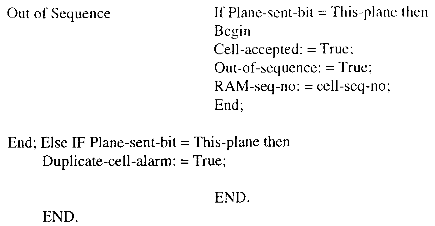
-
- Variables: cell-seq-no
- The sequence number of this incoming cell.
- RAM-seq-no
- The sequence number held in RAM for this VCI.
- Plane-sent-bit
- The Plane from which the last cell on this VCI was accepted.
- This-plane
- The plane that this cell has come from (0 or 1).
- Cell-accepted
- Control variable to say whether this cell is passed to the output FIFO.
- Duplicate-cell-alarm
- Indication to microprocessor that a cell which is duplicate of the last cell on this call on this plane has arrived.
- Out-of-sequence
- Indication to microprocessor that cells have been lost i.e. that cell sent out of sequence.
- The algorithm does not cause a modulo 64 sequence loss to occur due to the situation described above with respect to the prior art, and the performance in other situations is equal to that of previously used algorithms.
Claims (2)
- A method for identifying valid data cells comprising a call in a redundant path combining unit of an asynchronous transfer mode switch having duplicated switching planes, the method characterised in the steps of:-a) identifying the plane from which came the last accepted cell to be passed in respect of a particular call,b) checking that a sequence number associated with the current cell received is not greater by one than that for the last accepted cell which has been stored in a storage means (2),c) checking that the last accepted cell to be passed on the particular call was from the same plane as the current cell,d) checking if the current cell is a duplicate of the last accepted cell to arrive on this plane, and,e) passing the current cell to an output store (1) if c) is true and d) is not true and storing in the storage means (2) the sequence number of the current cell.
- Apparatus for executing the method claimed in Claim 1, comprising transceiver means arranged to receive and transmit data, a first store (1) connected to the transceiver means and, arranged to store plane identification data and cell sequence number data, a second store (2) arranged to store a call identifier (VCI) used to address the first store and a sequence number related to a particular cell, for presentation to an addressed location in the first store, first comparator (4), arranged to receive the sequence number from the second store (2) and a sequence number from the first store (1) and compare said sequence numbers, a second comparator (5) arranged to receive the sequence number from the second store (2), and the sequence number from the first store (1) by way of an incrementer (6) which is arranged to increment the sequence number by one, and compare said sequence numbers;means for identifying a switching plane from which came the last accepted cell to be passed in respect of a particular call and for identifying a switching plane from which came the current cell,means for providing a check signal when the current cell to be passed on the particular call was from the same plane as the last accepted cell and is not a duplicate thereof; andcell acceptance logic circuitry (3) connected to the first and second comparators (4, 5) and arranged to generate read control signals for the first store (1), in accordance with output signals generated by the first and second comparators (4, 5) and to generate write control signals for the first store (1) in accordance with output signals generated by the first and second comparators (4, 5) and a check signal generated by the means for providing same.
Priority Applications (1)
| Application Number | Priority Date | Filing Date | Title |
|---|---|---|---|
| DE1991632507 DE69132507T2 (en) | 1991-04-05 | 1991-04-05 | Method and device for identifying valid cells in a unit for combining redundant paths of an asynchronous transfer mode switching matrix |
Applications Claiming Priority (1)
| Application Number | Priority Date | Filing Date | Title |
|---|---|---|---|
| GB8922904A GB2236930B (en) | 1989-10-11 | 1989-10-11 | Method and apparatus for identifying valid cells in a redundant path combining unit of an asynchronous transfer mode switch |
Publications (2)
| Publication Number | Publication Date |
|---|---|
| EP0507022A1 EP0507022A1 (en) | 1992-10-07 |
| EP0507022B1 true EP0507022B1 (en) | 2001-01-10 |
Family
ID=10664401
Family Applications (1)
| Application Number | Title | Priority Date | Filing Date |
|---|---|---|---|
| EP91303027A Expired - Lifetime EP0507022B1 (en) | 1989-10-11 | 1991-04-05 | Method and apparatus for identifying valid cells in a redundant path combining unit of an asynchronous transfer mode switch |
Country Status (4)
| Country | Link |
|---|---|
| US (1) | US5278849A (en) |
| EP (1) | EP0507022B1 (en) |
| ES (1) | ES2153347T3 (en) |
| GB (1) | GB2236930B (en) |
Families Citing this family (16)
| Publication number | Priority date | Publication date | Assignee | Title |
|---|---|---|---|---|
| US5272696A (en) | 1992-01-23 | 1993-12-21 | Northern Telecom Limited | ATM plane merging filter for ATM switches and the method thereof |
| CA2110864C (en) * | 1992-12-08 | 1999-10-05 | Chikashi Itoh | Line accommodation circuit capable of switching from an active system to a standby system without a loss of a communication information signal |
| SE515421C2 (en) * | 1993-02-15 | 2001-07-30 | Ericsson Telefon Ab L M | Methods for handling redundant selector plan in package selector and selector for execution of the method |
| US5402415A (en) * | 1993-04-22 | 1995-03-28 | Washington University | Multicast virtual circuit switch using cell recycling |
| DE4331579C2 (en) * | 1993-09-16 | 1995-07-06 | Siemens Ag | Method for transmitting message cells over redundant virtual path pairs of an ATM communication network |
| US5588000A (en) * | 1995-03-27 | 1996-12-24 | Emulex Corporation | Apparatus for reordering data frames within an interface device |
| SE505091C2 (en) * | 1995-10-03 | 1997-06-23 | Ericsson Telefon Ab L M | Redundancy structure for digital voters |
| ATE389994T1 (en) * | 1997-03-27 | 2008-04-15 | Nokia Siemens Networks Gmbh | REDUNDANT TRANSMISSION SYSTEM WITH AVOIDANCE OF CELL REPEATS |
| ATE389995T1 (en) * | 1997-03-27 | 2008-04-15 | Nokia Siemens Networks Gmbh | REDUNDANT TRANSMISSION SYSTEM WITH SWITCHING OFF A TRANSMISSION ROUTE OF DEFECTIVE TRANSMISSION BEHAVIOR |
| AU9011898A (en) * | 1997-08-15 | 1999-03-08 | Telefonaktiebolaget Lm Ericsson (Publ) | Cell selection for atm switch having redundant switch planes |
| ES2240807T3 (en) * | 2001-09-26 | 2005-10-16 | Siemens Aktiengesellschaft | RECEPTION OF DATA MESSAGES IN COMMUNICATIONS SYSTEMS THAT INCLUDE ROUND NETWORK ROUTES. |
| GB2395096B (en) * | 2002-11-04 | 2004-11-10 | Roke Manor Research | Method of operating a redundant system |
| US7475142B2 (en) * | 2002-12-06 | 2009-01-06 | Cisco Technology, Inc. | CIFS for scalable NAS architecture |
| US7443845B2 (en) * | 2002-12-06 | 2008-10-28 | Cisco Technology, Inc. | Apparatus and method for a lightweight, reliable, packet-based transport protocol |
| EP3304790B1 (en) * | 2015-06-03 | 2022-03-09 | Hirschmann Automation and Control GmbH | Method for a redundant transmission system with prp and temporary storage of data packets |
| CN113312596B (en) * | 2021-06-10 | 2023-04-07 | 重庆市勘测院 | User identity recognition method based on deep learning and asynchronous track data |
Family Cites Families (5)
| Publication number | Priority date | Publication date | Assignee | Title |
|---|---|---|---|---|
| US4852127A (en) * | 1985-03-22 | 1989-07-25 | American Telephone And Telegraph Company, At&T Bell Laboratories | Universal protocol data receiver |
| JP2659421B2 (en) * | 1988-02-17 | 1997-09-30 | 日本電信電話株式会社 | Self-routing channel |
| JPH0286245A (en) * | 1988-09-21 | 1990-03-27 | Hitachi Ltd | Data link layer processing method |
| ATE107452T1 (en) * | 1989-03-03 | 1994-07-15 | Siemens Ag | METHOD AND CIRCUIT ARRANGEMENT FOR FORWARDING MESSAGE PACKETS TRANSMITTED ON SUPPLY CIRCUITS VIA A PACKET SWITCH. |
| US5163054A (en) * | 1990-12-31 | 1992-11-10 | International Business Machines Corp. | Method for data transmission using a modified high level data link control protocal |
-
1989
- 1989-10-11 GB GB8922904A patent/GB2236930B/en not_active Expired - Lifetime
-
1991
- 1991-03-28 US US07/676,172 patent/US5278849A/en not_active Expired - Lifetime
- 1991-04-05 ES ES91303027T patent/ES2153347T3/en not_active Expired - Lifetime
- 1991-04-05 EP EP91303027A patent/EP0507022B1/en not_active Expired - Lifetime
Also Published As
| Publication number | Publication date |
|---|---|
| GB2236930A (en) | 1991-04-17 |
| US5278849A (en) | 1994-01-11 |
| EP0507022A1 (en) | 1992-10-07 |
| GB8922904D0 (en) | 1989-11-29 |
| ES2153347T3 (en) | 2001-03-01 |
| GB2236930B (en) | 1994-03-23 |
Similar Documents
| Publication | Publication Date | Title |
|---|---|---|
| EP0507022A1 (en) | Method and apparatus for identifying valid cells in a redundant path combining unit of an asynchronous transfer mode switch | |
| CA2069346C (en) | Atm cell error processing system | |
| EP0683948B1 (en) | A method for handling redundant switching planes in packet switches and a packet switch for carrying out the method | |
| KR100237339B1 (en) | Resequencing Method and Apparatus | |
| US5200950A (en) | Method and circuit arrangement for reducing the loss of message packets that are transmitted via a packet switching equipment | |
| EP0603916B1 (en) | Packet switching system using idle/busy status of output buffers | |
| EP0379709B1 (en) | Single-fifo high speed combining switch | |
| KR100216371B1 (en) | Large scale atm switch with fault tolerant scheme and self routing method in 2nxn multiplexing switches | |
| CA2108863C (en) | Packet disassembler | |
| US6424632B1 (en) | Method and apparatus for testing packet data integrity using data check field | |
| US5729530A (en) | ATM switch | |
| US5222063A (en) | Method and circuit arrangement for reducing the loss of message packets that are transmitted via a packet switching equipment | |
| JPH0575639A (en) | ATM switch path test method | |
| US5153920A (en) | Method and circuit arrangement for the acceptance and forwarding of message cells transmitted according to an asynchronous transfer mode by an asynchronous transfer mode switching equipment | |
| EP0683949B1 (en) | A method for handling redundant switching planes in packet switches and a switch for carrying out the method | |
| EP0523571A1 (en) | Advanced code error detection apparatus and system using maximal-length pseudorandom binary sequence | |
| WO1998044686A2 (en) | Method and device in telecommunications system | |
| CA2233121C (en) | Redundant transmission system with diconnection of a transmission path exhibiting faulty transmission behavior | |
| AU631066B2 (en) | Transmission quality assessment arrangement | |
| JPH0653942A (en) | Apparatus for generation and inspection of error correction code of message in message changeover system | |
| CA2039223A1 (en) | Method and apparatus for identifying valid cells in a redundant path combining unit of an asynchronous transfer mode switch | |
| JP3335646B2 (en) | Method and apparatus for valid cell identification in redundant path coupling unit of asynchronous transfer mode switch | |
| IE911050A1 (en) | Method and apparatus for identifying valid cells in a¹redundant path combining unit of an asynchronous transfer¹mode switch | |
| US5724353A (en) | Self-routing switch method and circuit for an ATM switch | |
| JP2824483B2 (en) | Switch diagnostic method in ATM exchange |
Legal Events
| Date | Code | Title | Description |
|---|---|---|---|
| PUAI | Public reference made under article 153(3) epc to a published international application that has entered the european phase |
Free format text: ORIGINAL CODE: 0009012 |
|
| AK | Designated contracting states |
Kind code of ref document: A1 Designated state(s): BE DE DK ES FR GR IT LU NL SE |
|
| 17P | Request for examination filed |
Effective date: 19930405 |
|
| 17Q | First examination report despatched |
Effective date: 19950413 |
|
| RAP1 | Party data changed (applicant data changed or rights of an application transferred) |
Owner name: GPT LIMITED |
|
| RAP1 | Party data changed (applicant data changed or rights of an application transferred) |
Owner name: MARCONI COMMUNICATIONS LIMITED |
|
| GRAG | Despatch of communication of intention to grant |
Free format text: ORIGINAL CODE: EPIDOS AGRA |
|
| GRAG | Despatch of communication of intention to grant |
Free format text: ORIGINAL CODE: EPIDOS AGRA |
|
| GRAG | Despatch of communication of intention to grant |
Free format text: ORIGINAL CODE: EPIDOS AGRA |
|
| GRAH | Despatch of communication of intention to grant a patent |
Free format text: ORIGINAL CODE: EPIDOS IGRA |
|
| GRAH | Despatch of communication of intention to grant a patent |
Free format text: ORIGINAL CODE: EPIDOS IGRA |
|
| GRAA | (expected) grant |
Free format text: ORIGINAL CODE: 0009210 |
|
| AK | Designated contracting states |
Kind code of ref document: B1 Designated state(s): BE DE DK ES FR GR IT LU NL SE |
|
| PG25 | Lapsed in a contracting state [announced via postgrant information from national office to epo] |
Ref country code: SE Free format text: THE PATENT HAS BEEN ANNULLED BY A DECISION OF A NATIONAL AUTHORITY Effective date: 20010110 Ref country code: GR Free format text: LAPSE BECAUSE OF NON-PAYMENT OF DUE FEES Effective date: 20010110 |
|
| ITF | It: translation for a ep patent filed | ||
| ET | Fr: translation filed | ||
| REF | Corresponds to: |
Ref document number: 69132507 Country of ref document: DE Date of ref document: 20010215 |
|
| REG | Reference to a national code |
Ref country code: ES Ref legal event code: FG2A Ref document number: 2153347 Country of ref document: ES Kind code of ref document: T3 |
|
| PG25 | Lapsed in a contracting state [announced via postgrant information from national office to epo] |
Ref country code: LU Free format text: LAPSE BECAUSE OF NON-PAYMENT OF DUE FEES Effective date: 20010405 |
|
| PG25 | Lapsed in a contracting state [announced via postgrant information from national office to epo] |
Ref country code: DK Free format text: LAPSE BECAUSE OF FAILURE TO SUBMIT A TRANSLATION OF THE DESCRIPTION OR TO PAY THE FEE WITHIN THE PRESCRIBED TIME-LIMIT Effective date: 20010410 |
|
| PLBE | No opposition filed within time limit |
Free format text: ORIGINAL CODE: 0009261 |
|
| STAA | Information on the status of an ep patent application or granted ep patent |
Free format text: STATUS: NO OPPOSITION FILED WITHIN TIME LIMIT |
|
| 26N | No opposition filed | ||
| PGFP | Annual fee paid to national office [announced via postgrant information from national office to epo] |
Ref country code: ES Payment date: 20020417 Year of fee payment: 12 |
|
| PGFP | Annual fee paid to national office [announced via postgrant information from national office to epo] |
Ref country code: BE Payment date: 20020627 Year of fee payment: 12 |
|
| PG25 | Lapsed in a contracting state [announced via postgrant information from national office to epo] |
Ref country code: ES Free format text: LAPSE BECAUSE OF NON-PAYMENT OF DUE FEES Effective date: 20030407 |
|
| PG25 | Lapsed in a contracting state [announced via postgrant information from national office to epo] |
Ref country code: BE Free format text: LAPSE BECAUSE OF NON-PAYMENT OF DUE FEES Effective date: 20030430 |
|
| BERE | Be: lapsed |
Owner name: *MARCONI COMMUNICATIONS LTD Effective date: 20030430 |
|
| NLS | Nl: assignments of ep-patents |
Owner name: MARCONI UK INTELLECTUAL PROPERTY LTD |
|
| REG | Reference to a national code |
Ref country code: FR Ref legal event code: TP |
|
| REG | Reference to a national code |
Ref country code: ES Ref legal event code: FD2A Effective date: 20030407 |
|
| NLS | Nl: assignments of ep-patents |
Owner name: M (DGP1) LTD Effective date: 20060802 Owner name: ERICSSON AB Effective date: 20060802 |
|
| REG | Reference to a national code |
Ref country code: FR Ref legal event code: TP |
|
| PGFP | Annual fee paid to national office [announced via postgrant information from national office to epo] |
Ref country code: IT Payment date: 20080429 Year of fee payment: 18 |
|
| PGFP | Annual fee paid to national office [announced via postgrant information from national office to epo] |
Ref country code: FR Payment date: 20100506 Year of fee payment: 20 |
|
| PGFP | Annual fee paid to national office [announced via postgrant information from national office to epo] |
Ref country code: DE Payment date: 20100428 Year of fee payment: 20 Ref country code: NL Payment date: 20100424 Year of fee payment: 20 |
|
| PG25 | Lapsed in a contracting state [announced via postgrant information from national office to epo] |
Ref country code: IT Free format text: LAPSE BECAUSE OF NON-PAYMENT OF DUE FEES Effective date: 20090405 |
|
| REG | Reference to a national code |
Ref country code: DE Ref legal event code: R071 Ref document number: 69132507 Country of ref document: DE |
|
| REG | Reference to a national code |
Ref country code: NL Ref legal event code: V4 Effective date: 20110405 |
|
| PG25 | Lapsed in a contracting state [announced via postgrant information from national office to epo] |
Ref country code: NL Free format text: LAPSE BECAUSE OF EXPIRATION OF PROTECTION Effective date: 20110405 |
|
| PG25 | Lapsed in a contracting state [announced via postgrant information from national office to epo] |
Ref country code: DE Free format text: LAPSE BECAUSE OF EXPIRATION OF PROTECTION Effective date: 20110405 |