EP0505531B1 - Power supply for generating an output voltage mainly of sinusoidal shape - Google Patents
Power supply for generating an output voltage mainly of sinusoidal shape Download PDFInfo
- Publication number
- EP0505531B1 EP0505531B1 EP91916711A EP91916711A EP0505531B1 EP 0505531 B1 EP0505531 B1 EP 0505531B1 EP 91916711 A EP91916711 A EP 91916711A EP 91916711 A EP91916711 A EP 91916711A EP 0505531 B1 EP0505531 B1 EP 0505531B1
- Authority
- EP
- European Patent Office
- Prior art keywords
- power supply
- voltage
- output voltage
- output
- control device
- Prior art date
- Legal status (The legal status is an assumption and is not a legal conclusion. Google has not performed a legal analysis and makes no representation as to the accuracy of the status listed.)
- Expired - Lifetime
Links
- 239000004065 semiconductor Substances 0.000 claims abstract description 15
- 239000003990 capacitor Substances 0.000 claims description 12
- 238000005259 measurement Methods 0.000 claims description 10
- 238000009499 grossing Methods 0.000 claims 1
- 239000004020 conductor Substances 0.000 description 21
- 238000010586 diagram Methods 0.000 description 6
- 230000001939 inductive effect Effects 0.000 description 2
- 238000000034 method Methods 0.000 description 2
- 238000004804 winding Methods 0.000 description 2
- CYJRNFFLTBEQSQ-UHFFFAOYSA-N 8-(3-methyl-1-benzothiophen-5-yl)-N-(4-methylsulfonylpyridin-3-yl)quinoxalin-6-amine Chemical compound CS(=O)(=O)C1=C(C=NC=C1)NC=1C=C2N=CC=NC2=C(C=1)C=1C=CC2=C(C(=CS2)C)C=1 CYJRNFFLTBEQSQ-UHFFFAOYSA-N 0.000 description 1
- 230000004913 activation Effects 0.000 description 1
- 230000007423 decrease Effects 0.000 description 1
- 230000003111 delayed effect Effects 0.000 description 1
- 230000006870 function Effects 0.000 description 1
- 230000006698 induction Effects 0.000 description 1
Images

Classifications
-
- H—ELECTRICITY
- H02—GENERATION; CONVERSION OR DISTRIBUTION OF ELECTRIC POWER
- H02H—EMERGENCY PROTECTIVE CIRCUIT ARRANGEMENTS
- H02H3/00—Emergency protective circuit arrangements for automatic disconnection directly responsive to an undesired change from normal electric working condition with or without subsequent reconnection ; integrated protection
- H02H3/02—Details
- H02H3/06—Details with automatic reconnection
Definitions
- the present invention refers to a power supply and more specifically of the kind by which it is possible to generate a mainly sinusoidal voltage to be used in supplying apparatuses that are normally operated from the mains.
- Such a power supply could be comprised by a unit generating a DC voltage and being associated with a DC/AC converter which, by means of switching technique known in the art, converts the DC voltage to a mainly sinusoidal AC voltage of the desired magnitude, for example 110 volts or 220 volts.
- the DC voltage generating unit could be a three-phase AC generator of the kind to be found in cars for their electric supply.
- a generator of the kind referred to comprises a rectifying device providing a DC voltage output from the generator.
- Such a generator together with a DC/AC converter constructed by means of known technique can be provided in the engine compartment of a car or motor caravan and be terminated with an AC outlet. Then, by a suitable line the living part of the motor caravan or a caravan connected to the car can be supplied.
- a power supply of the kind referred to has to be protected against excess current and to this end protecting arrangements are provided which disconnect the power supply when the load current exceeds a predetermined value.
- the art offers a solution where in case of a disconnection reconnection is allowed after the lapse of a time period corresponding to one or two periods of the AC voltage. If inductive loads, such as an induction motor of a refrigerator or an air conditioner, are to be supplied the delayed reconnection is a disadvantage as sufficient energy will not be supplied to the motor to have it rotate before disconnection takes place due to overcurrent. Hence, under certain conditions it may happen that the compressor motor in the refrigerator or in the air conditioner, respectively, cannot be started.
- the object of the invention is to remedy the drawback indicated and to provide a power supply of the kind referred to above at which reconnection takes place after a time period which is considerably smaller as compared to half the period of the AC voltage. This means that reconnection takes place almost immediately after a disconnection has occurred so that there will be no substantial drop of current below the predermined current limit. Hence, the current is upheld and sufficient energy supplied for bringing the motor to start.
- the object is achieved in a power supply according to the invention which has been given the characterizing features indicated in the appended claim 1. Preferred embodiments are included in the sub-claims.
- FIG. 1 there is shown a block diagram for a power supply according to the invention in which an AC generator 10 is provided which, via a rectifier device 11, generates a DC voltage U across a positive terminal 12 and a negative terminal 13. A conductor 14 is connected to the positive terminal 12 while a conductor 15 is connected to the negative terminal 13.
- the generator 10 has a field winding 16 and the voltage U is controlled by a control device 17 which, upon need, increases or decreases the voltage to the field winding 16.
- the circuit of fig. i further comprises an DC/AC converter 18 in which are included four semiconductor switches of the mosfet type 19,20,21,22, in a known way forming a bridge.
- Conductors 23 and 24 connect the connecting points with one respective choking coil 25,26 the opposite ends of which are interconnected by a capacitor 27 and, further, are connected to two terminals 28,29 forming the output terminals of the power supply.
- a control device 30 is provided for supplying to the semiconductor switches 19,20,21,22 suitable commutating signals according to a predetermined program. According to this program each of the half periods of the sinusoidal output voltage is assumed to be divided into sections and for each section a combination of commutating signals is stored which for the respective section determines which switches are to be closed and which are to be open in order for the output voltage to assume the desired sinusoidal shape. How to carry out this in practice will be described more in detail below in connection with Fig. 2.
- a bank of capacitors is provided, here represented by a capacitor C which is connected to conductor 14 and, via a low-resistant measurement resistor R to conductor 15.
- the voltage across the measurement resistor 15 forms a parameter which depends on the load current of the power supply and which is used to switch off the supply when overcurrent occurs.
- the connecting point between the measurement resistor R and the capacitor C is connected to a block 33 in which the voltage is compared with a reference value. If the voltage exceeds said reference value a signal is emitted from the block 33 to the control device 30 causing cancellation of the commutating signals to the semiconductor switches 19,20,21,22.
- this disconnection is very short and is followed, almoast immediately, by a reconnection of the commutating signals. This will be described more in detail in connection with Fig. 2.
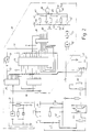
- Fig. 2 In order to create combinations of control signals for setting of the four semiconductor switches in each section of the sinusoidal output voltage to be formed, in a known way, simultaneously a sine wave and the invers of it are compared with a triangular wave having the same amplitude as the sine waves but being of a considerably higher frequency. Briefly, the condition for the switches to open for the supply of energy is that the triangular wave is within the envelope formed by the sine waves.
- the two half periods of the sine wave are divided into a number of sections and for each section a combination of control signals is set to control which of the switches are to be open and which are to be closed, respectively, in said section.
- the combinations of control signals for all sections are stored in a programmable memory 34 and each combination comprises eight digital bits.
- Each combination has a 16-bit address and the combinations are arranged in the memory such that they can be emitted in the order that causes the desired sinusoidal shape of the output voltage to be formed.
- the combinations are read from the memory 34 by means of a counter 35,36 stepped by means of an oscillator 37 operating at the frequency of 3.27 MHz.
- a low-resistant measurement resistor R is being connected in series with the bank of capacitors C and the voltage appearing across the resistor is, via a filter comprising two resistors 41,42 and a capacitor 43, led to the input of an opto switch 44.
- the output of the opto switch is connected to ground via a resistor 45 in parallel with a capacitor 46. Said output is also connected to the RESET-input of a flip-flop 47.
- the clock input C1 of the flip-flop is, via a conductor 48, connected to an output of the counter 35,36 chosen such that the the clock frequency is about 2 kHz. Via a conductor 49, the output of the flip-flop is connected to one input of an AND-gate 50.
- the other input of the AND-gate is connected to the supply voltage +5 volts.
- the output of the AND-gate is, via an inverter 51 and a buffer circuit 52, connected to one input of the AND-gate 40, at the output 53 of which one of the bits of a digital control signal for the semiconductor switches appears.
- the other input of the AND-gate 40 is, via a conductor 54, connected to the output of a buffer circuit 55, the input of which , via a conductor 56, is connected to one of the outputs of the clamping circuit 38.
- the clamping circuit is controlled by clock pulses supplied to a clock input CLK from an output of the counter 35,36 via a conductor 57, an inverter 58 and another conductor 59. Further, via a conductor 60, one of the outputs of the clamping circuit 38 is connected to the input of a buffer circuit 61 the output of which, via a conductor 62, being connected to one input of the AND-gate 39. The other input of the AND-gate 39 is connected to a conductor 63 interconnecting the corresponding inputs of all eight AND-gates, of which only two 39,40 have been shown, said conductor 63 being connected to the output of the buffer circuit 52.
- the conductors 54 and 62 are, via the respective resistors 64,65, connected to a conductor 66 connected to the supply voltage +15 volts.
- Fig. 1 The function of the embodiment generally shown in Fig. 1 and more in detail in Fig. 2 will now be described. It is assumed that the generator 10 is rotating, for example driven by the motor of a motor caravan, and that the voltage U is established across the conductors 14 and 15. Now, in a way not shown, also the supply voltages for the electronic components are generated, such as those marked +5 volts and +15 volts.
- the oscillator 37 is operating and feeds clock pulses of the frequency of 3.27 MHz to the counter 35,36 (two cases). In operation, the counter is always counting-up until it reaches its highest count position from which it recommences. For each step an address is given to the memory 34 and the contents of this address is fed to the clamping circuit 38.
- said contents is an eight-bit digital combination of control signals for the semiconductor switches 19,20,21,22 (Fig. 1) determining which of the switches to be closed and which to be open in a predetermined section in any of the half periods of the sinusoidal output voltage.
- the clamping circuit 38 feeds its information to the AND-gates 39,40 (and to the remaining six AND-gates, not shown) and the states at the outputs of the AND-gates constitute the desired control information for the semiconductor switches. Accordingly, as the counter is continuously stepped up those various combinations of control signals will be emitted, one upon the other, which are required to give to the output voltage the desired sinusoidal shape.
Landscapes
- Inverter Devices (AREA)
- Rectifiers (AREA)
- Ac-Ac Conversion (AREA)
- Dc-Dc Converters (AREA)
Abstract
Description
- The present invention refers to a power supply and more specifically of the kind by which it is possible to generate a mainly sinusoidal voltage to be used in supplying apparatuses that are normally operated from the mains.
- Such a power supply is known from EP-A-227849. This document discloses all the features of the preamble of the appended claim 1.
- In caravans and motor caravans electric apparatuses and other equipment are to be found which are operated by low voltage DC current, for example from a car battery or the like. In addition, there is often other equipment which is operated from the mains and which can be used only when the caravan is connected to the mains, for example at a caravan site.
- Now, it is desired to provide a power supply by which it will be possible to use mains operated equipment even in the case the caravan is not situated at a caravan site, or the like, and, accordingly, cannot be connected to the mains. Such a power supply could be comprised by a unit generating a DC voltage and being associated with a DC/AC converter which, by means of switching technique known in the art, converts the DC voltage to a mainly sinusoidal AC voltage of the desired magnitude, for example 110 volts or 220 volts. Suitably, the DC voltage generating unit could be a three-phase AC generator of the kind to be found in cars for their electric supply. A generator of the kind referred to comprises a rectifying device providing a DC voltage output from the generator. Such a generator together with a DC/AC converter constructed by means of known technique can be provided in the engine compartment of a car or motor caravan and be terminated with an AC outlet. Then, by a suitable line the living part of the motor caravan or a caravan connected to the car can be supplied.
- A power supply of the kind referred to has to be protected against excess current and to this end protecting arrangements are provided which disconnect the power supply when the load current exceeds a predetermined value. The art offers a solution where in case of a disconnection reconnection is allowed after the lapse of a time period corresponding to one or two periods of the AC voltage. If inductive loads, such as an induction motor of a refrigerator or an air conditioner, are to be supplied the delayed reconnection is a disadvantage as sufficient energy will not be supplied to the motor to have it rotate before disconnection takes place due to overcurrent. Hence, under certain conditions it may happen that the compressor motor in the refrigerator or in the air conditioner, respectively, cannot be started.
- The object of the invention is to remedy the drawback indicated and to provide a power supply of the kind referred to above at which reconnection takes place after a time period which is considerably smaller as compared to half the period of the AC voltage. This means that reconnection takes place almost immediately after a disconnection has occurred so that there will be no substantial drop of current below the predermined current limit. Hence, the current is upheld and sufficient energy supplied for bringing the motor to start. The object is achieved in a power supply according to the invention which has been given the characterizing features indicated in the appended claim 1. Preferred embodiments are included in the sub-claims.
- The invention will now be described more in detail in connection with an embodiment and with reference to the enclosed drawinings in which:
- Fig. 1
- is a block diagram for a power supply according to the invention, and
- Fig. 2
- is a practical circuit diagram for a preferred embodiment in which parts inessential to the invention have been omitted.
- In Fig. 1 there is shown a block diagram for a power supply according to the invention in which an
AC generator 10 is provided which, via arectifier device 11, generates a DC voltage U across apositive terminal 12 and anegative terminal 13. Aconductor 14 is connected to thepositive terminal 12 while aconductor 15 is connected to thenegative terminal 13. Thegenerator 10 has a field winding 16 and the voltage U is controlled by acontrol device 17 which, upon need, increases or decreases the voltage to the field winding 16. - The circuit of fig. i further comprises an DC/
AC converter 18 in which are included four semiconductor switches of themosfet type transistors transistors Conductors respective choking coil capacitor 27 and, further, are connected to twoterminals - A
control device 30 is provided for supplying to thesemiconductor switches - In order to maintain the voltage level during varying load conditions, in a known way a bank of capacitors is provided, here represented by a capacitor C which is connected to
conductor 14 and, via a low-resistant measurement resistor R toconductor 15. The voltage across themeasurement resistor 15 forms a parameter which depends on the load current of the power supply and which is used to switch off the supply when overcurrent occurs. Hence, the connecting point between the measurement resistor R and the capacitor C is connected to ablock 33 in which the voltage is compared with a reference value. If the voltage exceeds said reference value a signal is emitted from theblock 33 to thecontrol device 30 causing cancellation of the commutating signals to thesemiconductor switches - Leaving the block diagram of Fig. 1 we are now turning to a practical circuit diagram shown in Fig. 2. In order to create combinations of control signals for setting of the four semiconductor switches in each section of the sinusoidal output voltage to be formed, in a known way, simultaneously a sine wave and the invers of it are compared with a triangular wave having the same amplitude as the sine waves but being of a considerably higher frequency. Briefly, the condition for the switches to open for the supply of energy is that the triangular wave is within the envelope formed by the sine waves.
- As made apparent from the above, the two half periods of the sine wave are divided into a number of sections and for each section a combination of control signals is set to control which of the switches are to be open and which are to be closed, respectively, in said section. The combinations of control signals for all sections are stored in a programmable memory 34 and each combination comprises eight digital bits. Each combination has a 16-bit address and the combinations are arranged in the memory such that they can be emitted in the order that causes the desired sinusoidal shape of the output voltage to be formed. The combinations are read from the memory 34 by means of a
counter oscillator 37 operating at the frequency of 3.27 MHz. In order to ensure that all bits of a combination be correctly read in time the bits so read are accumulated in aclamping circuit 38 from which the bits are clocked to eight AND-gates of which only two, 39,40, have been shown in the circuit diagram. Then, at the outputs of the AND-gates those control signals appear which determine the switching state of the four semiconductor switches. The way these control signals are shaped and supplied to the switches and the type of switch chosen or the way of arranging the switches are inessential to the invention and, hence, will not be described in detail. - As in Fig. 1, in order to detect overcurrent a low-resistant measurement resistor R is being connected in series with the bank of capacitors C and the voltage appearing across the resistor is, via a filter comprising two
resistors capacitor 43, led to the input of anopto switch 44. The output of the opto switch is connected to ground via aresistor 45 in parallel with a capacitor 46. Said output is also connected to the RESET-input of a flip-flop 47. The clock input C1 of the flip-flop is, via a conductor 48, connected to an output of thecounter conductor 49, the output of the flip-flop is connected to one input of an AND-gate 50. The other input of the AND-gate is connected to the supply voltage +5 volts. The output of the AND-gate is, via aninverter 51 and abuffer circuit 52, connected to one input of the AND-gate 40, at theoutput 53 of which one of the bits of a digital control signal for the semiconductor switches appears. The other input of the AND-gate 40 is, via a conductor 54, connected to the output of abuffer circuit 55, the input of which , via aconductor 56, is connected to one of the outputs of theclamping circuit 38. - The clamping circuit is controlled by clock pulses supplied to a clock input CLK from an output of the
counter conductor 57, aninverter 58 and anotherconductor 59. Further, via aconductor 60, one of the outputs of theclamping circuit 38 is connected to the input of abuffer circuit 61 the output of which, via aconductor 62, being connected to one input of the AND-gate 39. The other input of the AND-gate 39 is connected to aconductor 63 interconnecting the corresponding inputs of all eight AND-gates, of which only two 39,40 have been shown, saidconductor 63 being connected to the output of thebuffer circuit 52. Theconductors 54 and 62 are, via therespective resistors conductor 66 connected to the supply voltage +15 volts. - The function of the embodiment generally shown in Fig. 1 and more in detail in Fig. 2 will now be described. It is assumed that the
generator 10 is rotating, for example driven by the motor of a motor caravan, and that the voltage U is established across theconductors oscillator 37 is operating and feeds clock pulses of the frequency of 3.27 MHz to thecounter 35,36 (two cases). In operation, the counter is always counting-up until it reaches its highest count position from which it recommences. For each step an address is given to the memory 34 and the contents of this address is fed to the clampingcircuit 38. As has been previously mentioned, said contents is an eight-bit digital combination of control signals for the semiconductor switches 19,20,21,22 (Fig. 1) determining which of the switches to be closed and which to be open in a predetermined section in any of the half periods of the sinusoidal output voltage. Upon a clock signal being emitted from thecounter conductor 57 theclamping circuit 38 feeds its information to the AND-gates 39,40 (and to the remaining six AND-gates, not shown) and the states at the outputs of the AND-gates constitute the desired control information for the semiconductor switches. Accordingly, as the counter is continuously stepped up those various combinations of control signals will be emitted, one upon the other, which are required to give to the output voltage the desired sinusoidal shape. - If a current which is larger than can be handled by the power supply is drawn by a load the current through the measurement resistor R, flowing towards to capacitor C, will cause a voltage to be established across the input of the
opto switch 44 which is sufficient for generating a flow of light in said opto switch which activates a light-sensitive diod causing a transistor to be activated which gives high level at the output of the opto switch. As a result, the flip-flop 47 is reset giving a high level at the output of the AND-gate 50, low level at the output of theinverter 51 and low level at the output of thebuffer circuit 52. Hence, one input of the AND-gates 39,40 (and of the remaining six) will take a low level causing all control signals to be stopped. - After a time period of about 0.5 milliseconds (corresponding to the frequency 2 kHz) a clock pulse appears on the conductor 48 which sets the flip-
flop 47 and causes a low level at one input of the AND-gate 50. As a result, the inputs of the AND-gates 39,40 connected to theconductor 63 will again take a high level. Accordingly, information from the clampingcircuit 38 can again pass the AND-gates 39,40 for the control of the semiconductor switches. Hence, the reconnection of the switches takes place after a short period of time, of the magnitude of 0.5 milliseconds, which is well within the half period of 10 milliseconds where overcurrent was detected and the power supply switched off. If overcurrent should again be detected several reconnections can be made within a half period of the output voltage permitting activation of inductive loads, such as motors and the like which can be started and driven from the power supply described. In a load as referred to the start current is high whereas the continuous working current is considerably lower. Such repeated restarts take place at intervals determined by the clock pulse frequency of about 2 kHz, mentioned above.
Claims (6)
- Power supply for generating a mainly sinusoidal output voltage the magnitude and frequency of which being adapted for the driving of apparatuses supplied from the mains, comprising means (10) for generating a DC voltage, a DC/AC converter (18) including controlled semiconductor switches (19,20,21,22), and an electric control device (30) emitting to the semiconductor switches suitable commutating signals in accordance with a predetermined program to keep said switches open and closed, respectively, such that the desired shape of the output voltage be achieved, means (R) being provided for sensing of a parameter associated with the load current of the power supply, said means (R) cooperating with the control device (30) such that when the load current exceeds a predetermined value the commutating signals are cancelled, said commutating signals being reconnected after a break which is considerably less than half the period of the output voltage, said power supply being characterized in that said control device (30) is arranged to continuously emit commutating signals with said breaks determined by the load current exceeding the predetermined value.
- Power supply according to claim 1, characterized in that at normal mains frequency of 50 Hz or 60 Hz the frequency of reconnection is about 2 kHz.
- Power supply according to claim 1, characterized in that the DC voltage generating means (10) has an output with two output terminals (12,13) and comprises a smoothing capacitor (C) connected in series with a low-resistant measurement resistor (R) across the output terminals (12,13), the voltage across the measurement resistor (R) constituting the paramenter associated with the load current.
- Power supply according to claim 1, characterized in that the electric control device (30) comprises a memory (34) in which the predetermined program is stored in such way that for the forming of the output voltage consecutive combinations of closed and open semiconductor switches, respectively, have corresponding consecutive addresses in the memory, and counter means (35,36) are arranged to read out the combinations by being stepwise counted up and in each step to transfer the respective combination to a clamping circuit (38) from which the combination is being clocked to a logic network comprising a number of AND-gates (39,40 etc.) so that each bit of the combination appears as a logical signal at one input of the respective AND-gates (39,40 etc.) while at the other input a signal appears which during normal operation permits the transfer of the combinations to the semiconductor switches and upon overcurrent determines the frequency of reconnection.
- Power supply according to claims 3 and 4, characterized in that the measurement resistor (R) is connected to the input of an opto switch (44) the output of which is connected to a flip-flop (47) such that upon overcurrent the flip-flop is resetted, the output signal of the flip-flop being transferred to the remaining inputs of the AND-gates (39,40 etc.) connected to the clamping circuit (38) via suitable gate means (50,51) for the purpose of applying a low level on same thereby preventing commutating signals from being generated.
- Power supply according to claim 5, characterized in that the input of the opto switch (44) is connected to the measurement resistor (R) via a filter comprising a capacitor (43) i series with two resistors (41,42), connected to each respective side of the capacitor, said capacitor being connected to said input and the free ends of the respective resistor being connected to the respective terminal of the measurement resistor (R).
Applications Claiming Priority (3)
| Application Number | Priority Date | Filing Date | Title |
|---|---|---|---|
| SE9002937A SE467130B (en) | 1990-09-14 | 1990-09-14 | POWER SUPPLY FOR GENERATION OF A PRINCIPLY SINUS SHAPED RISK |
| SE9002937 | 1990-09-14 | ||
| PCT/SE1991/000602 WO1992005610A1 (en) | 1990-09-14 | 1991-09-11 | Power supply for generating an output voltage mainly of sinusoidal shape |
Publications (2)
| Publication Number | Publication Date |
|---|---|
| EP0505531A1 EP0505531A1 (en) | 1992-09-30 |
| EP0505531B1 true EP0505531B1 (en) | 1995-09-13 |
Family
ID=20380363
Family Applications (1)
| Application Number | Title | Priority Date | Filing Date |
|---|---|---|---|
| EP91916711A Expired - Lifetime EP0505531B1 (en) | 1990-09-14 | 1991-09-11 | Power supply for generating an output voltage mainly of sinusoidal shape |
Country Status (6)
| Country | Link |
|---|---|
| US (1) | US5278747A (en) |
| EP (1) | EP0505531B1 (en) |
| DE (1) | DE69113019T2 (en) |
| ES (1) | ES2078544T3 (en) |
| SE (1) | SE467130B (en) |
| WO (1) | WO1992005610A1 (en) |
Families Citing this family (11)
| Publication number | Priority date | Publication date | Assignee | Title |
|---|---|---|---|---|
| US5372045A (en) * | 1993-02-12 | 1994-12-13 | Rosemount Inc. | Bridge pulse controlled constant current driver for magnetic flowmeter |
| JPH08111988A (en) * | 1994-08-15 | 1996-04-30 | Toshiba Corp | Power converter |
| US5537367A (en) * | 1994-10-20 | 1996-07-16 | Lockwood; Geoffrey R. | Sparse array structures |
| EP0954091A1 (en) * | 1998-04-28 | 1999-11-03 | Giovanni Brugnettini | Compact mechanical-electrical transducer |
| DE19834315A1 (en) * | 1998-07-30 | 2000-02-03 | Ako Werke Gmbh & Co | Circuit arrangement for measuring and limiting currents in converters for feeding motors |
| US6243276B1 (en) | 1999-05-07 | 2001-06-05 | S-B Power Tool Company | Power supply system for battery operated devices |
| WO2002043064A2 (en) * | 2000-11-27 | 2002-05-30 | Seagate Technology Llc | Motor start-up current control apparatus and method |
| KR100636749B1 (en) * | 2004-10-15 | 2006-10-19 | 주식회사 현대오토넷 | Vehicle AC Power Supply |
| FI119493B (en) * | 2006-12-21 | 2008-11-28 | Vacon Oyj | Arrangements for measuring the current through a frequency converter |
| US10784700B2 (en) | 2010-10-15 | 2020-09-22 | Nextek Power Systems, Inc. | Arrangement for and method of dynamically managing electrical power between an electrical power source and an electrical load |
| WO2018204045A1 (en) * | 2017-04-13 | 2018-11-08 | Nextek Power Systems, Inc. | Arrangement for and method of dynamically managing electrical power between an electrical power source and an electrical load |
Family Cites Families (12)
| Publication number | Priority date | Publication date | Assignee | Title |
|---|---|---|---|---|
| US3914675A (en) * | 1973-09-17 | 1975-10-21 | Gen Electric | Fault detector circuit for electric vehicle control |
| NL175755C (en) * | 1978-10-31 | 1984-12-17 | Wavin Bv | FLANGE TUBE PART BOTH OF FIBER-REINFORCED THERMO-CURING RESIN AND METHOD FOR PRODUCING SUCH A FLANGE TUBE PART. |
| US4447841A (en) * | 1982-06-30 | 1984-05-08 | Motorola Inc. | Overcurrent protection circuit for a multiple output switching power supply and method therefor |
| US4521840A (en) * | 1983-02-14 | 1985-06-04 | Borg-Warner Corporation | D-C Bus current monitoring system |
| JPS60134781A (en) * | 1983-12-23 | 1985-07-18 | Matsushita Electric Ind Co Ltd | Malfunction detector of air conditioner |
| US4706177A (en) * | 1985-11-14 | 1987-11-10 | Elliot Josephson | DC-AC inverter with overload driving capability |
| US4719555A (en) * | 1985-12-19 | 1988-01-12 | Hitachi, Ltd. | Electric power control apparatus with first and second fixed time intervals |
| CA1287103C (en) * | 1986-04-22 | 1991-07-30 | Jim Pinard | Cmos latch-up recovery circuit |
| JPS6434180A (en) * | 1987-07-27 | 1989-02-03 | Toshiba Corp | Controlling device of power converter |
| US4809122A (en) * | 1987-07-31 | 1989-02-28 | Brunswick Corporation | Self-protective fuel pump driver circuit |
| JPH01166484U (en) * | 1988-05-16 | 1989-11-21 | ||
| US5029269A (en) * | 1990-04-12 | 1991-07-02 | Rockwell International Corporation | Delayed power supply overvoltage shutdown apparatus |
-
1990
- 1990-09-14 SE SE9002937A patent/SE467130B/en not_active IP Right Cessation
-
1991
- 1991-09-11 WO PCT/SE1991/000602 patent/WO1992005610A1/en not_active Ceased
- 1991-09-11 EP EP91916711A patent/EP0505531B1/en not_active Expired - Lifetime
- 1991-09-11 ES ES91916711T patent/ES2078544T3/en not_active Expired - Lifetime
- 1991-09-11 US US07/849,421 patent/US5278747A/en not_active Expired - Fee Related
- 1991-09-11 DE DE69113019T patent/DE69113019T2/en not_active Expired - Fee Related
Also Published As
| Publication number | Publication date |
|---|---|
| SE9002937D0 (en) | 1990-09-14 |
| WO1992005610A1 (en) | 1992-04-02 |
| DE69113019D1 (en) | 1995-10-19 |
| DE69113019T2 (en) | 1996-04-04 |
| SE467130B (en) | 1992-05-25 |
| ES2078544T3 (en) | 1995-12-16 |
| US5278747A (en) | 1994-01-11 |
| EP0505531A1 (en) | 1992-09-30 |
| SE9002937L (en) | 1992-03-15 |
Similar Documents
| Publication | Publication Date | Title |
|---|---|---|
| US6232742B1 (en) | Dc/ac inverter apparatus for three-phase and single-phase motors | |
| EP1336528B1 (en) | Ground fault detection system and method | |
| US5574346A (en) | On and off state fault detection circuit for a multi-phase brushed or brushless DC motor | |
| US6630751B2 (en) | Excessive load capacitor detection circuit for UPS | |
| US4672520A (en) | Current-source power converting apparatus with self-extinction devices | |
| US5278747A (en) | DC/AC converter with overcurrent protection by temporary shutdown | |
| JP3751024B2 (en) | Triac control circuit | |
| JP2000505997A (en) | High voltage AC to low voltage DC converter | |
| JP2008061496A (en) | Pwm method for cycloconverter | |
| JPH08308253A (en) | Switching semiconductor device | |
| JPH08336281A (en) | Residual voltage protection device for electric circuit | |
| US5737163A (en) | DC-AC converter protection | |
| EP0479196B1 (en) | Power supply circuit | |
| US5222012A (en) | Power management circuit for a magnetic repulsion punch | |
| JP3574599B2 (en) | Inrush current prevention circuit with input overvoltage limit function | |
| JPH10176643A (en) | Capacitor charge / discharge igniter | |
| EP0547006B1 (en) | Self-oscillating circuit for driving a gas discharge lamp, particularly for use on board a motor vehicle | |
| JP3284526B2 (en) | Instantaneous voltage drop compensator | |
| JPH03280619A (en) | Power element driving circuit | |
| JPH08221141A (en) | Power supply circuit | |
| WO1997030569A1 (en) | In-rush surge limiting electronic ballast | |
| JP3273814B2 (en) | Open phase detection circuit | |
| US4172278A (en) | DC to AC inverter | |
| JPH0898552A (en) | Power supply | |
| EP0007920B1 (en) | Auxiliary commutation circuit for an inverter |
Legal Events
| Date | Code | Title | Description |
|---|---|---|---|
| PUAI | Public reference made under article 153(3) epc to a published international application that has entered the european phase |
Free format text: ORIGINAL CODE: 0009012 |
|
| 17P | Request for examination filed |
Effective date: 19920513 |
|
| AK | Designated contracting states |
Kind code of ref document: A1 Designated state(s): DE ES FR GB IT SE |
|
| 17Q | First examination report despatched |
Effective date: 19940406 |
|
| GRAA | (expected) grant |
Free format text: ORIGINAL CODE: 0009210 |
|
| AK | Designated contracting states |
Kind code of ref document: B1 Designated state(s): DE ES FR GB IT SE |
|
| ITF | It: translation for a ep patent filed | ||
| REF | Corresponds to: |
Ref document number: 69113019 Country of ref document: DE Date of ref document: 19951019 |
|
| PG25 | Lapsed in a contracting state [announced via postgrant information from national office to epo] |
Ref country code: SE Effective date: 19951213 |
|
| REG | Reference to a national code |
Ref country code: ES Ref legal event code: FG2A Ref document number: 2078544 Country of ref document: ES Kind code of ref document: T3 |
|
| ET | Fr: translation filed | ||
| PLBE | No opposition filed within time limit |
Free format text: ORIGINAL CODE: 0009261 |
|
| STAA | Information on the status of an ep patent application or granted ep patent |
Free format text: STATUS: NO OPPOSITION FILED WITHIN TIME LIMIT |
|
| 26N | No opposition filed | ||
| PGFP | Annual fee paid to national office [announced via postgrant information from national office to epo] |
Ref country code: FR Payment date: 19960910 Year of fee payment: 6 |
|
| PGFP | Annual fee paid to national office [announced via postgrant information from national office to epo] |
Ref country code: ES Payment date: 19960927 Year of fee payment: 6 |
|
| PG25 | Lapsed in a contracting state [announced via postgrant information from national office to epo] |
Ref country code: ES Free format text: LAPSE BECAUSE OF THE APPLICANT RENOUNCES Effective date: 19970912 |
|
| PG25 | Lapsed in a contracting state [announced via postgrant information from national office to epo] |
Ref country code: FR Free format text: THE PATENT HAS BEEN ANNULLED BY A DECISION OF A NATIONAL AUTHORITY Effective date: 19970930 |
|
| REG | Reference to a national code |
Ref country code: FR Ref legal event code: ST |
|
| REG | Reference to a national code |
Ref country code: ES Ref legal event code: FD2A Effective date: 20001102 |
|
| REG | Reference to a national code |
Ref country code: GB Ref legal event code: IF02 |
|
| PGFP | Annual fee paid to national office [announced via postgrant information from national office to epo] |
Ref country code: GB Payment date: 20020911 Year of fee payment: 12 |
|
| PGFP | Annual fee paid to national office [announced via postgrant information from national office to epo] |
Ref country code: DE Payment date: 20020918 Year of fee payment: 12 |
|
| PG25 | Lapsed in a contracting state [announced via postgrant information from national office to epo] |
Ref country code: GB Free format text: LAPSE BECAUSE OF NON-PAYMENT OF DUE FEES Effective date: 20030911 |
|
| PG25 | Lapsed in a contracting state [announced via postgrant information from national office to epo] |
Ref country code: DE Free format text: LAPSE BECAUSE OF NON-PAYMENT OF DUE FEES Effective date: 20040401 |
|
| GBPC | Gb: european patent ceased through non-payment of renewal fee |
Effective date: 20030911 |
|
| PG25 | Lapsed in a contracting state [announced via postgrant information from national office to epo] |
Ref country code: IT Free format text: LAPSE BECAUSE OF NON-PAYMENT OF DUE FEES;WARNING: LAPSES OF ITALIAN PATENTS WITH EFFECTIVE DATE BEFORE 2007 MAY HAVE OCCURRED AT ANY TIME BEFORE 2007. THE CORRECT EFFECTIVE DATE MAY BE DIFFERENT FROM THE ONE RECORDED. Effective date: 20050911 |