EP0504851A2 - Semiconductor optical device - Google Patents
Semiconductor optical device Download PDFInfo
- Publication number
- EP0504851A2 EP0504851A2 EP92104703A EP92104703A EP0504851A2 EP 0504851 A2 EP0504851 A2 EP 0504851A2 EP 92104703 A EP92104703 A EP 92104703A EP 92104703 A EP92104703 A EP 92104703A EP 0504851 A2 EP0504851 A2 EP 0504851A2
- Authority
- EP
- European Patent Office
- Prior art keywords
- substrate
- rod
- rods
- light
- laser
- Prior art date
- Legal status (The legal status is an assumption and is not a legal conclusion. Google has not performed a legal analysis and makes no representation as to the accuracy of the status listed.)
- Granted
Links
Images




Classifications
-
- H—ELECTRICITY
- H10—SEMICONDUCTOR DEVICES; ELECTRIC SOLID-STATE DEVICES NOT OTHERWISE PROVIDED FOR
- H10H—INORGANIC LIGHT-EMITTING SEMICONDUCTOR DEVICES HAVING POTENTIAL BARRIERS
- H10H20/00—Individual inorganic light-emitting semiconductor devices having potential barriers, e.g. light-emitting diodes [LED]
- H10H20/80—Constructional details
- H10H20/81—Bodies
- H10H20/819—Bodies characterised by their shape, e.g. curved or truncated substrates
- H10H20/821—Bodies characterised by their shape, e.g. curved or truncated substrates of the light-emitting regions, e.g. non-planar junctions
-
- B—PERFORMING OPERATIONS; TRANSPORTING
- B82—NANOTECHNOLOGY
- B82Y—SPECIFIC USES OR APPLICATIONS OF NANOSTRUCTURES; MEASUREMENT OR ANALYSIS OF NANOSTRUCTURES; MANUFACTURE OR TREATMENT OF NANOSTRUCTURES
- B82Y20/00—Nanooptics, e.g. quantum optics or photonic crystals
-
- G—PHYSICS
- G02—OPTICS
- G02B—OPTICAL ELEMENTS, SYSTEMS OR APPARATUS
- G02B6/00—Light guides; Structural details of arrangements comprising light guides and other optical elements, e.g. couplings
- G02B6/24—Coupling light guides
- G02B6/42—Coupling light guides with opto-electronic elements
- G02B6/4201—Packages, e.g. shape, construction, internal or external details
- G02B6/4202—Packages, e.g. shape, construction, internal or external details for coupling an active element with fibres without intermediate optical elements, e.g. fibres with plane ends, fibres with shaped ends, bundles
-
- H—ELECTRICITY
- H01—ELECTRIC ELEMENTS
- H01S—DEVICES USING THE PROCESS OF LIGHT AMPLIFICATION BY STIMULATED EMISSION OF RADIATION [LASER] TO AMPLIFY OR GENERATE LIGHT; DEVICES USING STIMULATED EMISSION OF ELECTROMAGNETIC RADIATION IN WAVE RANGES OTHER THAN OPTICAL
- H01S5/00—Semiconductor lasers
- H01S5/10—Construction or shape of the optical resonator, e.g. extended or external cavity, coupled cavities, bent-guide, varying width, thickness or composition of the active region
- H01S5/12—Construction or shape of the optical resonator, e.g. extended or external cavity, coupled cavities, bent-guide, varying width, thickness or composition of the active region the resonator having a periodic structure, e.g. in distributed feedback [DFB] lasers
- H01S5/1228—DFB lasers with a complex coupled grating, e.g. gain or loss coupling
-
- H—ELECTRICITY
- H01—ELECTRIC ELEMENTS
- H01S—DEVICES USING THE PROCESS OF LIGHT AMPLIFICATION BY STIMULATED EMISSION OF RADIATION [LASER] TO AMPLIFY OR GENERATE LIGHT; DEVICES USING STIMULATED EMISSION OF ELECTROMAGNETIC RADIATION IN WAVE RANGES OTHER THAN OPTICAL
- H01S5/00—Semiconductor lasers
- H01S5/10—Construction or shape of the optical resonator, e.g. extended or external cavity, coupled cavities, bent-guide, varying width, thickness or composition of the active region
- H01S5/18—Surface-emitting [SE] lasers, e.g. having both horizontal and vertical cavities
- H01S5/183—Surface-emitting [SE] lasers, e.g. having both horizontal and vertical cavities having only vertical cavities, e.g. vertical cavity surface-emitting lasers [VCSEL]
-
- H—ELECTRICITY
- H01—ELECTRIC ELEMENTS
- H01S—DEVICES USING THE PROCESS OF LIGHT AMPLIFICATION BY STIMULATED EMISSION OF RADIATION [LASER] TO AMPLIFY OR GENERATE LIGHT; DEVICES USING STIMULATED EMISSION OF ELECTROMAGNETIC RADIATION IN WAVE RANGES OTHER THAN OPTICAL
- H01S5/00—Semiconductor lasers
- H01S5/40—Arrangement of two or more semiconductor lasers, not provided for in groups H01S5/02 - H01S5/30
- H01S5/4025—Array arrangements, e.g. constituted by discrete laser diodes or laser bar
- H01S5/4031—Edge-emitting structures
-
- H—ELECTRICITY
- H10—SEMICONDUCTOR DEVICES; ELECTRIC SOLID-STATE DEVICES NOT OTHERWISE PROVIDED FOR
- H10H—INORGANIC LIGHT-EMITTING SEMICONDUCTOR DEVICES HAVING POTENTIAL BARRIERS
- H10H20/00—Individual inorganic light-emitting semiconductor devices having potential barriers, e.g. light-emitting diodes [LED]
- H10H20/01—Manufacture or treatment
- H10H20/011—Manufacture or treatment of bodies, e.g. forming semiconductor layers
- H10H20/013—Manufacture or treatment of bodies, e.g. forming semiconductor layers having light-emitting regions comprising only Group III-V materials
-
- H—ELECTRICITY
- H01—ELECTRIC ELEMENTS
- H01S—DEVICES USING THE PROCESS OF LIGHT AMPLIFICATION BY STIMULATED EMISSION OF RADIATION [LASER] TO AMPLIFY OR GENERATE LIGHT; DEVICES USING STIMULATED EMISSION OF ELECTROMAGNETIC RADIATION IN WAVE RANGES OTHER THAN OPTICAL
- H01S3/00—Lasers, i.e. devices using stimulated emission of electromagnetic radiation in the infrared, visible or ultraviolet wave range
- H01S3/05—Construction or shape of optical resonators; Accommodation of active medium therein; Shape of active medium
- H01S3/06—Construction or shape of active medium
- H01S3/063—Waveguide lasers, i.e. whereby the dimensions of the waveguide are of the order of the light wavelength
- H01S3/067—Fibre lasers
- H01S3/06708—Constructional details of the fibre, e.g. compositions, cross-section, shape or tapering
-
- H—ELECTRICITY
- H01—ELECTRIC ELEMENTS
- H01S—DEVICES USING THE PROCESS OF LIGHT AMPLIFICATION BY STIMULATED EMISSION OF RADIATION [LASER] TO AMPLIFY OR GENERATE LIGHT; DEVICES USING STIMULATED EMISSION OF ELECTROMAGNETIC RADIATION IN WAVE RANGES OTHER THAN OPTICAL
- H01S5/00—Semiconductor lasers
- H01S5/0014—Measuring characteristics or properties thereof
- H01S5/0028—Laser diodes used as detectors
-
- H—ELECTRICITY
- H01—ELECTRIC ELEMENTS
- H01S—DEVICES USING THE PROCESS OF LIGHT AMPLIFICATION BY STIMULATED EMISSION OF RADIATION [LASER] TO AMPLIFY OR GENERATE LIGHT; DEVICES USING STIMULATED EMISSION OF ELECTROMAGNETIC RADIATION IN WAVE RANGES OTHER THAN OPTICAL
- H01S5/00—Semiconductor lasers
- H01S5/02—Structural details or components not essential to laser action
- H01S5/0206—Substrates, e.g. growth, shape, material, removal or bonding
- H01S5/0217—Removal of the substrate
-
- H—ELECTRICITY
- H01—ELECTRIC ELEMENTS
- H01S—DEVICES USING THE PROCESS OF LIGHT AMPLIFICATION BY STIMULATED EMISSION OF RADIATION [LASER] TO AMPLIFY OR GENERATE LIGHT; DEVICES USING STIMULATED EMISSION OF ELECTROMAGNETIC RADIATION IN WAVE RANGES OTHER THAN OPTICAL
- H01S5/00—Semiconductor lasers
- H01S5/06—Arrangements for controlling the laser output parameters, e.g. by operating on the active medium
- H01S5/0607—Arrangements for controlling the laser output parameters, e.g. by operating on the active medium by varying physical parameters other than the potential of the electrodes, e.g. by an electric or magnetic field, mechanical deformation, pressure, light, temperature
- H01S5/0608—Arrangements for controlling the laser output parameters, e.g. by operating on the active medium by varying physical parameters other than the potential of the electrodes, e.g. by an electric or magnetic field, mechanical deformation, pressure, light, temperature controlled by light, e.g. optical switch
-
- H—ELECTRICITY
- H01—ELECTRIC ELEMENTS
- H01S—DEVICES USING THE PROCESS OF LIGHT AMPLIFICATION BY STIMULATED EMISSION OF RADIATION [LASER] TO AMPLIFY OR GENERATE LIGHT; DEVICES USING STIMULATED EMISSION OF ELECTROMAGNETIC RADIATION IN WAVE RANGES OTHER THAN OPTICAL
- H01S5/00—Semiconductor lasers
- H01S5/10—Construction or shape of the optical resonator, e.g. extended or external cavity, coupled cavities, bent-guide, varying width, thickness or composition of the active region
- H01S5/1042—Optical microcavities, e.g. cavity dimensions comparable to the wavelength
-
- H—ELECTRICITY
- H01—ELECTRIC ELEMENTS
- H01S—DEVICES USING THE PROCESS OF LIGHT AMPLIFICATION BY STIMULATED EMISSION OF RADIATION [LASER] TO AMPLIFY OR GENERATE LIGHT; DEVICES USING STIMULATED EMISSION OF ELECTROMAGNETIC RADIATION IN WAVE RANGES OTHER THAN OPTICAL
- H01S5/00—Semiconductor lasers
- H01S5/20—Structure or shape of the semiconductor body to guide the optical wave ; Confining structures perpendicular to the optical axis, e.g. index or gain guiding, stripe geometry, broad area lasers, gain tailoring, transverse or lateral reflectors, special cladding structures, MQW barrier reflection layers
- H01S5/22—Structure or shape of the semiconductor body to guide the optical wave ; Confining structures perpendicular to the optical axis, e.g. index or gain guiding, stripe geometry, broad area lasers, gain tailoring, transverse or lateral reflectors, special cladding structures, MQW barrier reflection layers having a ridge or stripe structure
- H01S5/223—Buried stripe structure
-
- H—ELECTRICITY
- H01—ELECTRIC ELEMENTS
- H01S—DEVICES USING THE PROCESS OF LIGHT AMPLIFICATION BY STIMULATED EMISSION OF RADIATION [LASER] TO AMPLIFY OR GENERATE LIGHT; DEVICES USING STIMULATED EMISSION OF ELECTROMAGNETIC RADIATION IN WAVE RANGES OTHER THAN OPTICAL
- H01S5/00—Semiconductor lasers
- H01S5/30—Structure or shape of the active region; Materials used for the active region
- H01S5/34—Structure or shape of the active region; Materials used for the active region comprising quantum well or superlattice structures, e.g. single quantum well [SQW] lasers, multiple quantum well [MQW] lasers or graded index separate confinement heterostructure [GRINSCH] lasers
- H01S5/341—Structures having reduced dimensionality, e.g. quantum wires
- H01S5/3412—Structures having reduced dimensionality, e.g. quantum wires quantum box or quantum dash
-
- H—ELECTRICITY
- H01—ELECTRIC ELEMENTS
- H01S—DEVICES USING THE PROCESS OF LIGHT AMPLIFICATION BY STIMULATED EMISSION OF RADIATION [LASER] TO AMPLIFY OR GENERATE LIGHT; DEVICES USING STIMULATED EMISSION OF ELECTROMAGNETIC RADIATION IN WAVE RANGES OTHER THAN OPTICAL
- H01S5/00—Semiconductor lasers
- H01S5/40—Arrangement of two or more semiconductor lasers, not provided for in groups H01S5/02 - H01S5/30
- H01S5/4006—Injection locking
-
- H—ELECTRICITY
- H01—ELECTRIC ELEMENTS
- H01S—DEVICES USING THE PROCESS OF LIGHT AMPLIFICATION BY STIMULATED EMISSION OF RADIATION [LASER] TO AMPLIFY OR GENERATE LIGHT; DEVICES USING STIMULATED EMISSION OF ELECTROMAGNETIC RADIATION IN WAVE RANGES OTHER THAN OPTICAL
- H01S5/00—Semiconductor lasers
- H01S5/40—Arrangement of two or more semiconductor lasers, not provided for in groups H01S5/02 - H01S5/30
- H01S5/4025—Array arrangements, e.g. constituted by discrete laser diodes or laser bar
- H01S5/4031—Edge-emitting structures
- H01S5/4056—Edge-emitting structures emitting light in more than one direction
-
- H—ELECTRICITY
- H01—ELECTRIC ELEMENTS
- H01S—DEVICES USING THE PROCESS OF LIGHT AMPLIFICATION BY STIMULATED EMISSION OF RADIATION [LASER] TO AMPLIFY OR GENERATE LIGHT; DEVICES USING STIMULATED EMISSION OF ELECTROMAGNETIC RADIATION IN WAVE RANGES OTHER THAN OPTICAL
- H01S5/00—Semiconductor lasers
- H01S5/40—Arrangement of two or more semiconductor lasers, not provided for in groups H01S5/02 - H01S5/30
- H01S5/42—Arrays of surface emitting lasers
- H01S5/423—Arrays of surface emitting lasers having a vertical cavity
-
- H—ELECTRICITY
- H01—ELECTRIC ELEMENTS
- H01S—DEVICES USING THE PROCESS OF LIGHT AMPLIFICATION BY STIMULATED EMISSION OF RADIATION [LASER] TO AMPLIFY OR GENERATE LIGHT; DEVICES USING STIMULATED EMISSION OF ELECTROMAGNETIC RADIATION IN WAVE RANGES OTHER THAN OPTICAL
- H01S5/00—Semiconductor lasers
- H01S5/50—Amplifier structures not provided for in groups H01S5/02 - H01S5/30
- H01S5/5045—Amplifier structures not provided for in groups H01S5/02 - H01S5/30 the arrangement having a frequency filtering function
Definitions
- the present invention relates to a semiconductor optical device and, more particularly, to a semiconductor optical device suitable for use as a light-emitting diode or a laser for coherent optical communications.
- a distributed feedback semiconductor laser In order to improve directionality and wavelength selectivity of light in the light-emitting semiconductor device, i.e., the light-emitting diode and laser, a distributed feedback semiconductor laser has been proposed. There has also been proposed a so-called micro-cavity laser as a semiconductor laser provided in an extremely small structure. For example, in a micro-cavity laser having a structure comparable to a wavelength, as described in Extended abstracts (the 43rd Autumn Meeting (1982)), the Japan Society of Applied Physics, and related Society, 29a-B-6, p.
- An object of the present invention is to eliminate the demerits in the above described distributed feedback semiconductor laser and to provide a semiconductor optical device with high directionality and wavelength selectivity of light.
- Another object of the present invention is to provide a micro-cavity laser which can be manufactured easily and with good reproducibility.
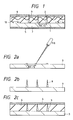
- nanowhiskers having a pn junction on the surface of a semiconductor substrate 3 as shown in FIG. 1.
- the nanowhisker is formed of an n-type region 1 and a p-type region 2 and a plurality of the same are arranged at intervals of an integer multiple of the wavelength as shown in FIG. 1. Accordingly, emitted light from the pn junction of each of the nanowhiskers superimpose on each other and, as a result, the so-called laser beam excellent in directionality and wave selectivity of light is emitted sideways.
- nanowhiskers in which defects are hardly produced are used in the present invention, a great advantage is obtained that a laser of higher quality than the conventional distributed feedback semiconductor lasers can be provided.
- the interval between nanowhiskers in a desired direction is set to be different from an integer multiple of the wavelength, light is not emitted in that direction.
- the wavelength ⁇ is compensated for the refractive index of the dielectric through which the light propagates.
- the micro-cavity laser of the present invention is formed of a semiconductor rod smaller than 1 ⁇ m in diameter and the electrical property of the semiconductor rod changes from n-type to p-type in the middle of the rod. Its structure is shown in FIG. 22, in which an example if a semiconductor rod formed of p-GaAs and n-GaAs. With the micro-cavity laser structured in the described manner, since the refractive index inside the rod as a resonator becomes higher than that outside the same and the size is very small, only an extremely small number of eigen modes are allowed to exist and the so-called low-threshold value laser can be realized.
- the direction of the length of the rod to be in the direction of the crystal axis (111) of the direct transition semiconductor crystal, good symmetry of the crystal is obtained and more effective laser can be lased.
- the semiconductor rod 201 is buried in the core 202 of an optical fiber 203 for optical communication as shown in FIG. 23, light is effectively introduced into the optical fiber 203 and a much greater merit than before can be obtained from the optical fiber s a medium for optical transmission.
- a method to realize such a semiconductor rod is to use a very thin semiconductor crystal epitaxially grown on a semiconductor substrate. More specifically, as shown in FIG. 24, a very thin semiconductor crystal 205 of GaAs, for example, is formed by epitaxial growth from the substrate 204 and, in the course of the epitaxial growth, the species of the ion for doping is changed, for example from n-type to p-type, and thereby the micro-cavity laser can be produced.
- a thin crystal whose diameter periodically changes along the length in the course of growth may be used, with the period of the changing diameter set to be equal to one half the wavelength, and then, a distributed feedback amplification type semiconductor laser can be obtained.
- the distance from one light-emitting rod to the adjoining light-emitting rod is an integer multiple of the wavelength ⁇ of the emitted laser beam.
- a beam with the wavelength ⁇ outgoing from a light-emitting rod induces excitons within another light-emitting rod and thus a beam with the wavelength ⁇ being in phase can be lased.
- a plurality of light-emitting rods 9 are arranged in a regular n-polygon configuration as shown in FIG. 15, then light beams are radiated in the directions of all the sides from the respective light-emitting rods. If an optical device of the configuration in which a plurality of light-emitting rods are arranged as described above is used as an optical antenna, it becomes possible to capture electromagnetic waves propagating from all directions in the two-dimensional space.
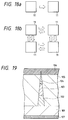
- each of the optical devices 11 When two optical devices 11 are arranged as shown in FIG. 18a and one is supplied with power so as to operate as a laser oscillator throwing its laser beam to the other, the other device operates as a receiver.
- transmission and reception of signals between the optical devices as shown in 18b can be realized.
- each of the optical devices is provided with feedback system and adapted to once convert an electromagnetic wave propagated from the surroundings into electricity and then convert the electricity into a light beam through its own optical device to irradiate another optical device with the light beam, the devices will freely communicate with each other and such an arrangement will be applicable to a neural network.
- micro-cavity laser according to the present invention is very small in size being of the order of a wavelength, a laser having a low threshold value or a coherent light-emitting device or a coherent LED having no threshold value can be obtained.
- the radius is as small as less than 1 ⁇ m and the length is comparable to the wavelength of the light, all of the light waves have an extremely small number of eigen resonant modes. Accordingly, not only induced transition but also spontaneous emission processes are strictly controlled and hence a coherent light-emitting device or a coherent LED having no threshold value or a laser having a low threshold value can be formed. Besides, since the electrical property is changed from n-type to p-type in the middle of rod, light emission by injection of carriers occurs by the pn junction effect and, hence, lasing takes place.
- the rod 201 When the rod 201 is buried in an optical fiber 203 as shown in FIG. 23, the light beam emitted from the end face of the rod 201 is effectively confined in the optical fiber 202 and transmitted therethrough. Therefore, the coupling efficiency between the light source and the optical fiber is greatly improved over that in the conventional arrangements.
- Nanowhiskers were selectively grown on the plane of GaAs (111) B substrate by low-pressure metal organic vapor phase epitaxy and, thereby, a light-emitting rod was produced.
- FIB focused ion beams
- the metal forming eutectic with the semiconductor was implanted by FIB and the seeds from which crystals would grow were produced.
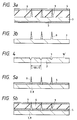
- nanowhiskers 9 were grown above the portions of the seeds as shown in FIG. 2b by low-pressure metal organic vapor phase epitaxy.
- Doping of the nanowhisker with impurities was performed such that, first, the nanowhisker was doped with an n-type impurity until it grew to a length of 2.1 ⁇ m and, then, the impurity was changed to a p-type impurity and therefrom the nanowhisker of p-type was allowed to grow another length of 2.1 ⁇ m. Accordingly, the nanowhisker is 4.2 ⁇ m long and has a pn junction formed just in its center. The doping concentration was set to 1018/cm3 for both the donor and the acceptor.
- SOG Spin-on-glass
- the SOG was cured by being held in a temperature of 480°C for 30 minutes and, thereby, an SOG film 6 being 4 ⁇ m thick was formed.
- the SOG stuck to the tip portion of the nanowhisker 9 was etched along a length of 0.2 ⁇ m by a hydrofluoric acid-system etchant and, thereby, the surface of the tip portion was exposed.
- a p-electrode 4 of a gold-zinc alloy film was formed above the tip portions by evaporation deposition and an ohmic contact was formed thereon by annealing the substrate under a temperature of 450°C.
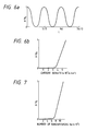
- the rear side of the substrate 3 was polished by fine polishing powder as shown in FIG. 3a, whereby total thickness was made to 100 ⁇ m.
- a gold-germanium-nickel film was deposited by evaporation on the rear surface of the substrate 3 to form an n-electrode 5.
- the substrate was then annealed under a temperature of 450°C and a laser oscillator as shown in FIG. 1 was produced. An electric field was applied to the laser oscillator and its characteristics were investigated.
- the laser oscillator shown in FIG. 1 was obtained by linearly arranging the nanowhiskers obtained as described above. It was investigated under what conditions the oscillator can lase.
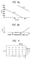
- FIG. 8b The relationship between the length of the substrate with the nanowhiskers one-dimensionally arranged thereon and the intensity of the oscillated laser beam (normalized power) P/P0 is shown in FIG. 8b. It was observed, as shown in FIG. 8b, the intensity of the oscillated laser beam sharply increased when the substrate length W exceeded approximately 20 cm. Further, representing the distance between adjoining nanowhiskers by L and the average thickness of the nanowhisker by W, the relationship between L and W at the time when lasing occurred was obtained as shown in FIG. 8a.
- the optical device as shown in the embodiment 1 was produced not using FIB but through the following process.
- an SiO2 film 10' was formed on a GaAs substrate 3 by a thermal CVD method to thickness of 0.1 ⁇ m. Then, holes 7 being 0.1 ⁇ m in diameter were made in the SiO2 film 10' by photolithography and vapor phase etching. The distance L between adjoining holes 7 was set to an integer multiple of semi-wavelength ( ⁇ /2). Above the holes 7, n-doped GaAs nanowhiskers were grown by an MOCVD method. Thereafter, the p-electrode and n-electrode were formed in the same way as in the embodiment 1. The micro-cavity laser formed through this process exhibited similar characteristics to those of the laser in the embodiment 1.
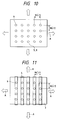
- a plurality of nanowhiskers 9 were arranged on the plane of the n-type GaAs (111) B substrate 3 so that the distance between adjoining nanowhiskers 9 would become an integer times as large as ⁇ /n2 as shown in FIG. 10 and SOG was applied onto the same.
- p-electrodes 4 were formed by evaporation along the rows or columns as shown in FIG. 11. Thereby, it became possible to cause only desired one row or one column of the nanowhiskers 9 to emit light. Further, by applying power only to one row or one column, an extremely narrow laser beam, whose width is comparable to the wavelength of the laser beam, could be obtained.
- the oscillated laser beams were observed only in the directions indicated by the arrows A in FIG. 10 and not observed in other directions because of attenuation due to interference of light.
- a plurality of nanowhiskers 9 were arranged on the plane of a GaAs (111) B semi-insulating substrate 8 so that the distance between adjoining nanowhiskers 9 would become an integer times as large as ⁇ /n2 as shown in FIG. 10 and then, before SOG was applied onto the substrate 8 with the nanowhiskers 9 formed thereon, n-electrodes 5 were formed as shown in FIG. 5a.
- a plurality of nanowhiskers 9 were arranged on the plane of a GaAs (111) B semi-insulating substrate 8 so that the distance between adjoining nanowhiskers 9 would become an integer times as large as ⁇ /n2 as shown in FIG. 10.
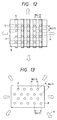
- n-electrodes 5 were formed on the substrate 8 in an array of rows or columns as shown in FIG. 5a and FIG. 12.
- the electrode material stuck to the nanowhisker 9 was easily removed by etching the same as in the embodiment 4.
- SOG 6 was applied and baked and, then, p-electrodes 4 were formed in the same way as in the embodiment 2.
- a plurality of nanowhiskers 9 were formed on the plane of a GaAs (111) B semi-insulating substrate 8 so that the distance between adjoining nanowhiskers 9 would become an integer times as large as ⁇ /n2 as shown in FIG. 13 and, then, electrodes were formed in the same way as in the embodiment 4. Laser beams were lased only in the directions as indicated by the arrows A in FIG. 13.
- a plurality of nanowhiskers were formed on the plane of a GaAs (111) B semi-insulating substrate 8 so that the distance between adjoining nanowhiskers 9 would become an integer times as large as ⁇ /n2 as shown in FIG. 14 and, then, electrodes were formed in the same way as in the embodiment 4. Laser beams were lased only in the directions as indicated by the arrows A in FIG. 14.
- a plurality of nanowhiskers 9 were formed on the plane of a GaAs (111) B semi-insulating substrate 8 so that the distance between adjoining nanowhiskers 9 in one direction would become an integer times as large as ⁇ /n2 and the distance in the other direction would become half the above value as shown in FIG. 9 and, then, electrodes were formed in the same way as in the embodiment 4. Laser beams were lased only in the directions as indicated by the arrows A in FIG. 9.
- An optical device was produced through the same process as that for the embodiment 5. However, a transparent electrode formed of an SnO2 film was used as the p-electrode 4 on the top surface of the device. The distance L between adjoining nanowhiskers 9 was set to N ⁇ '/2 . In the present embodiment, laser beams in the horizontal directions were not observed but a laser beam R was observed, instead, in the vertical direction as shown in FIG. 16a. The laser beam R was that having good coherence with an expanse comparable to the area of the electrode of the device, approximately 2.3 x 10⁴ ( ⁇ m2).
- An apparatus as shown in FIG. 16b was structured using the optical device produced by the method shown in the embodiment 2.
- a high voltage (1.5 V) was applied to this apparatus and a laser beam with a wavelength of around 860 nm lased from another semiconductor laser was transmitted through the apparatus.
- the laser beam R then emitted was better in coherence than the beam introduced therein.
- the optical device according to the present invention can be used not only as an oscillator but also as a resonator of laser beam.
- the incoming light pulse signal was correctly read by the optical device even if the incoming laser beam was changed variously.
- the optical devices read signals of electromagnetic wave transmitted from the surroundings and indicated the transmitted directions and power of the signals as electric signals.
- the device is equally usable though only the polarities of the electric characteristics are reversed.
- GaAs/AlGaAs hetero nanowhiskers were formed by an MOCVD method on an n-type GaAs (111) substrate 101 doped with Si in a density of 1019/cm3.
- Ga ions were implanted into specified regions in the substrate 101 by a focused ion beam method. As crystals are allowed to grow, the crystal growth selectively occurs only at the portion where the Ga ions were implanted. This phenomenon was utilized for producing nanowhiskers.
- the diameter of the Ga ion beam was set to 20nm so that the thickness of the crystal growing above it may become 20nm measured immediately above the substrate.
- an n-type AlGaAs crystal 102 doped with Si in a density of 1019/cm3 was grown.
- an i-type GaAs crystal 103 doped with no impurity was grown.
- a p-type AlGaAs crystal 104 doped with Zn in a density of 1019/cm3 was grown.
- Al content in the AlGaAs crystal was 0.1.
- the crystal growing times were set so that the lengths of the n-type and p-type AlGaAs crystals 102 and 104 both would become 100 nm.
- the length of the i-type GaAs crystal 103 was set to 30nm.
- an AlGaAs layer of which Al content was 0.2 was grown as a cap layer 105 to a thickness of 200 nm. Since the Al content of the cap layer 105 is higher than that of the nanowhisker portion, the current injected into the nanowhisker does not flow into the cap layer 105.
- the cap layer 105 not only the AlGaAs layer but also a transparent insulating member such as an SiO2 film or an SOG resin with a thickness of 200 nm can be used.
- the surface of the nanowhisker was dipped in a water solution of NH4S2, Li2S for 20 to 30 hours and, then, heated at a temperature of 50°C. Thereafter, the substrate was heated in hydrogen gas at a temperature of 390°C for 30 minutes. By this treatment, an oxide film on the surface of the nanowhisker is reduced and a good surface in which non-radiative electron-hole recombination is reduced can be obtained.
- the electrode for current injection was formed as follows. Au was deposited by evaporation on the rear surface of the substrate 101 to a thickness of 100 nm to thereby form a grounding electrode 107. Au/Zn alloy was deposited by evaporation on the surface of the cap layer 105 to a thickness of 100 nm and, thereby, the electrode for current injection 106 was formed. A forward voltage is applied to the pn junction within the nanowhisker through the electrode 106 and, thereby, the current injection can be achieved.
- a method for producing a nanowhisker having a pin junction in a hetero structure was described. It is possible to have an array of nanowhiskers well suited for use as a laser by controlling positions where focused ion beams are implanted, which will be described later in another embodiment.
- the nanowhisker having the hetero pin junction produced in the present embodiment can provide higher light-emitting efficiency than other nanowhiskers and the threshold current density can be reduced when a laser is formed of the same.
- an n-type substrate was used in the present embodiment described above, a hetero pin junction can be formed by a similar method even if a p-type substrate is used.
- the method for selectively growing nanowhiskers not only the method using the focused ion beam method but also the method using a mask pattern formed of an insulating film can be used. That is, first, an SiO2 film is formed on a substrate by the known sputtering method to a thickness of 50 nm and, then, a resist is applied onto the same and holes whose diameter is 20 nm are made therein by electron beam exposure, and then, nanowhiskers are grown at the hollowed portions. Thus, the positions where nanowhiskers grow can be specified.
- device was structured using GaAs and AlGaAs. Similar device can also be produced by using, as the substrate and the p-i-n portion, GaAs and GaAs-InAs-GaAs, or InP and InP-InGaAsP-InP, respectively.
- the substrate 3 can be cleaved into regular triangular form as shown in FIG. 20.
- the cleavage surfaces corresponding to the sides of the regular triangle will be denoted by X, Y, and Z.
- the array of the nanowhiskers 108 and treatment of the cleavage surfaces depend on the manner how the laser beam is taken out.
- the array of the nanowhiskers 108 is decided by setting the positions, where the focused ion beams mentioned in the embodiment 12 are implanted, as shown in FIG. 20.
- L1 denotes the distance between adjoining columns of the nanowhiskers parallel to the surface X and L2 denotes the distance between adjoining columns of the nanowhiskers perpendicular to the surface X.
- Nanowhiskers are formed by the method shown in the embodiments 12 and 13. However, the cleaving of the substrate is not yet done at this stage.
- a resist is applied onto a current injection electrode 106 described in the embodiment 12, the substrate is heated and an optical waveguide pattern of a transmission line form is formed by contact mask exposure, and chemical etching is performed using the pattern and, thereby, an optical waveguide type laser 113 is produced.
- the substrate is cleaved and a substrate 112 and a laser waveguide 113 as shown in FIG. 21 are obtained.
- the arrangement of nanowhiskers in the laser waveguide 113 is set to be corresponding to the arrangement given first in the embodiment 13.
- the end face of the waveguide is covered by a nonreflective coating film 114.
- a micro-cavity laser as shown in FIG. 22 was produced.
- ultra microcrystals 205 were grown by selective growth method on a GaAs (111) B semi-insulating substrate 204 as shown in FIG. 26a. More specifically, an SiO2 film 206 being 0.6 ⁇ m thick was formed on the GaAs substrate 204 by a thermal CVD method. Then, a plurality of holes whose diameter is 20 ⁇ M were made in the SiO2 film 206 by the known photolithographic technique.
- n-doped GaAs microcrystals 205 were grown by a metal organic chemical vapor deposition method (MOCVD method). The form of the crystal can be controlled by the growing conditions.
- MOCVD method metal organic chemical vapor deposition method
- the crystal Since the crystal has the property growing in the (111) direction, when the (111) B substrate 204 is used as in the present embodiment, the crystal grows in the direction perpendicular to the substrate 204 as shown in FIG. 26a.
- the microcrystal grown at this time was approximately 3 ⁇ m long.
- a p-GaAs microcrystal was successively grown under the same conditions as those used for growing the n-GaAs microcrystal.
- the growing time was similarly set to 20 minutes. As a result, the microcrystal 205 totally 6 ⁇ m long was formed.
- the grown microcrystals 205 were buried in a resin 207 as shown in FIG.
- microcrystals 205, together with the resin film 207 were taken out from the substrate 209, and then both sides of the resin film 207 were polished by very fine polishing agent so that a form with a thickness of 4 ⁇ m as shown in FIG. 26c was obtained.
- transparent SnO2 films 208 were formed on both sides and thereby a micro-cavity laser was produced.
- a low-threshold value laser was obtained, of which the threshold current value for lasing is as low as 1 ⁇ A.
- a micro-cavity laser having a structure as shown in FIG. 25 was produced.
- the method for manufacturing it is the same as that shown in the embodiment 16, but modulation growing was performed in this case in order to periodically vary the diameter in the longitudinal direction. More specifically, the ratio between V group dopant and III group dopant (V/III ratio) during the time of crystal growth was alternately changed between 18 and 22 every five minutes.
- the threshold current value for lasing the thus obtained micro-cavity laser was as low as 1 ⁇ A the same as in the embodiment 15, and the laser beam lased by the same, with the half-width being 1 MHz, was very good in coherence.
- micro-cavity laser 201 buried in the core 202 of an optical fiber 203 as shown in FIG. 23 was produced.
- micro-cavity lasers By producing micro-cavity lasers by the method shown in the embodiment 14, one of them was taken out and buried into the core 202 of a quartz optical fiber 203.
- minute holes were made in the optical fiber 203 sideways and lead wires 209 were taken out as shown in FIG. 27.
- its coupling efficiency with the optical fiber was very high as 90%.
- a micro-cavity laser similar to the embodiment 16 was produced.
- 50 layers of n-type GaAs 302 and n-type GaAlAs 303 were alternately piled up in the longitudinal direction on a GaAs substrate 301, then, above the same, an n-type Al 0.5 Ga 0.5 As layer 304, an In 0.2 Ga 0.8 As layer 305 including virtually no impurity, and a p-type Al 0.5 Ga 0.5 As layer 306 were piled, and further, above the same, 50 layers of p-type GaAs 308 and p-type GaAlAs 307 were alternately piled up, and thereby a semiconductor rod is formed.
- the film thickness of the n-type GaAs 302 and n-type GaAlAs 303 as well as the p-type GaAs 308 and p-type GaAlAs 307 were all set to a quarter of the emission wavelength.
- Electrodes (not shown) were provided at the top and bottom of the micro-cavity formed as described above. When current was passed through the electrodes longitudinally in the forward direction of the pn junction, a laser beam having good coherence similarly to that in the embodiment 16 was obtained.
- N-type GaAlAs was grown 1 ⁇ m in the longitudinal direction, and then, above the same, a GaAs layer including virtually no impurity was grown to a thickness of 2 nm, and, further, above the same, p-type GaAlAs was grown 1 ⁇ m, and, thereby, a plurality of semiconductor rods were formed. These semiconductor rods were arranged in an area of 2 ⁇ m square at a distance virtually equal to the diameter of the rod. Electrodes were provided at the top and bottom of the rods in order to pass current in the longitudinal direction. When a current was passed in the forward direction of the pn junction, a laser beam having very good coherence similarly to that in the embodiment 16 was obtained.
- FIG. 30 shows a schematic sectional view of a pn junction light-emitting device whose crystal surface was treated by sulfur (S) or selenium (Se) for its stabilization.
- reference numeral 401 denotes an n-type InP substrate
- 402 and 403 denote portions where a nanowhisker was formed.
- Reference numeral 404 denotes the treated layer for surface stabilization formed on the outer surface of the nanowhisker through the above described treatment with S or Se.
- Reference numeral 406, 407, and 408 denote the n-type region, undoped region and p-type region of the nanowhisker, respectively.
- the n-type region 406 is 1 ⁇ m long
- the p-type region 408 is 1 ⁇ m long
- the undoped region 407 is 10 nm long.
- 409 and 410 denote electrodes.
- D2 The thickness of the current transmission line 402 of the nanowhisker
- D1 is 20 nm and D2 is 15 nm.
- the thickness of the surface depletion layer 403 is reduced by 20 to 60% due to the existence of the treated layer 404 for surface stabilization. Accordingly, the thickness D2 of the current transmission line 402 of the nanowhisker is increased by 10 to 20% and, hence, it becomes 16 to 18 nm.
- a current 411 was passed, light emitted from the portion with the undoped region 407 in the center was observed.
- FIG. 31 A graph of relationship between emission gain of the light-emitting device and the emission wavelength is shown in FIG. 31.
- the curves a and b show the case where the surface stabilization treatment of the nanowhisker was performed and the case where the stabilization treatment was not performed, respectively.
- the working time is extremely prolonged by performing the surface stabilization treatment.
- the emission wavelength is shifted to the longer wavelength side by 0.05 ⁇ m or so from that of the curve b for the case where the surface stabilization treatment was not performed.
- the reason why the emission wavelength is shifted to the longer wavelength side when the surface stabilization treatment is performed is because the thickness of the depletion layer on the crystal surface is reduced and the width of the current transmission line where carriers are kept in is increased. On the other hand, the gain increased 1.5 to 2 times. This is because the rate of non-radiative recombination was reduced by the stabilization of the crystal surface.
- FIG. 32 shows dependence on working time of relative emission intensity in the present embodiment.
- the graph is the results of investigation of aged change of the peak emission intensity of the light-emitting device.
- the peak emission intensity gradually decreased with the working time in the range from 103 hours to 104 hours and it sharply decreased after 104 hours passed.
- the surface stabilization treatment was performed, as shown by the curve a, the peak emission intensity showed little change even in the range from 104 to 105 hours.
- the life span of the light-emitting device was prolonged more than 10 times by the surface stabilization treatment.
- a semiconductor laser can be realized by disposing semiconductor rods having a pn junction or a hetero junction at intervals of an integer multiple of the oscillation frequency and an optical antenna can be produced using the same apparatus.
- a micro-cavity laser whose threshold current is extremely small, as well as a coherent light-emitting device and coherent LED having no threshold value, can be formed, and therefore, key devices very effective for use in the field of optical communications can be obtained. This is because only a limited number of modes can contribute to lasing in the micro-cavity. Further, since the micro-cavity laser according to the present invention can be buried into the core of an optical fiber, it provides such a merit that the coupling efficiency between the optical fiber and the laser is greatly increased. Thus, great industrial advantages can be obtained from the present invention.
Landscapes
- Physics & Mathematics (AREA)
- Optics & Photonics (AREA)
- General Physics & Mathematics (AREA)
- Condensed Matter Physics & Semiconductors (AREA)
- Electromagnetism (AREA)
- Engineering & Computer Science (AREA)
- Nanotechnology (AREA)
- Chemical & Material Sciences (AREA)
- Biophysics (AREA)
- Crystallography & Structural Chemistry (AREA)
- Life Sciences & Earth Sciences (AREA)
- Semiconductor Lasers (AREA)
- Led Devices (AREA)
Abstract
Description
- The present invention relates to a semiconductor optical device and, more particularly, to a semiconductor optical device suitable for use as a light-emitting diode or a laser for coherent optical communications.
- In order to improve directionality and wavelength selectivity of light in the light-emitting semiconductor device, i.e., the light-emitting diode and laser, a distributed feedback semiconductor laser has been proposed. There has also been proposed a so-called micro-cavity laser as a semiconductor laser provided in an extremely small structure. For example, in a micro-cavity laser having a structure comparable to a wavelength, as described in Extended abstracts (the 43rd Autumn Meeting (1982)), the Japan Society of Applied Physics, and related Society, 29a-B-6, p. 127, all of the light waves are regulated by eigen (resonant) modes of extremely small number (several or zero), not only induced transition but also spontaneous emission process is extremely limited, and therefore, it becomes possible to realize novel optical devices such as coherent light-emitting devices or coherent LEDs with no threshold value and lasers with a very low threshold value.
- However, since the above distributed feedback semiconductor laser requires that a grating is formed on semiconductor substrate, crystalline defects are liable to be produced at the time of crystal growth. There have therefore been such demerits with it that a semiconductor laser of high quality is difficult to obtain. Further, since the micro-cavity laser requires very high level of techniques in its fabrication, it has been very difficult to actually produce lasers having uniform characteristics with good reproducibility.
- An object of the present invention is to eliminate the demerits in the above described distributed feedback semiconductor laser and to provide a semiconductor optical device with high directionality and wavelength selectivity of light.
- Another object of the present invention is to provide a micro-cavity laser which can be manufactured easily and with good reproducibility.
- In the present invention, in order to improve directionality and wavelength selectivity of light, there are formed nanowhiskers having a pn junction on the surface of a
semiconductor substrate 3 as shown in FIG. 1. The nanowhisker is formed of an n-type region 1 and a p-type region 2 and a plurality of the same are arranged at intervals of an integer multiple of the wavelength as shown in FIG. 1. Accordingly, emitted light from the pn junction of each of the nanowhiskers superimpose on each other and, as a result, the so-called laser beam excellent in directionality and wave selectivity of light is emitted sideways. At this time, since nanowhiskers in which defects are hardly produced are used in the present invention, a great advantage is obtained that a laser of higher quality than the conventional distributed feedback semiconductor lasers can be provided. - In the above, the case where a plurality of nanowhiskers are arranged one-dimensionally, i.e., linearly, was described. If a plurality of nanowhiskers are arranged on a plane at intervals of an integer multiple of the wavelength in each of two directions crossing each other at right angle, high quality laser beams can be obtained from two directions crossing at right angle, independently. This is a new function which has never been obtained from conventional distributed feedback semiconductor lasers. By arranging nanowhiskers at intervals of an integer multiple of the wavelength in desired two directions other than those orthogonal to each other, laser beams emitted in such desired directions can be obtained and the use of the device can be remarkably expanded. On the other hand, if the interval between nanowhiskers in a desired direction is set to be different from an integer multiple of the wavelength, light is not emitted in that direction. The interval L most effectively preventing light from being emitted in that direction is

- The micro-cavity laser of the present invention is formed of a semiconductor rod smaller than 1 µm in diameter and the electrical property of the semiconductor rod changes from n-type to p-type in the middle of the rod. Its structure is shown in FIG. 22, in which an example if a semiconductor rod formed of p-GaAs and n-GaAs. With the micro-cavity laser structured in the described manner, since the refractive index inside the rod as a resonator becomes higher than that outside the same and the size is very small, only an extremely small number of eigen modes are allowed to exist and the so-called low-threshold value laser can be realized.
- Further, by selecting the direction of the length of the rod to be in the direction of the crystal axis (111) of the direct transition semiconductor crystal, good symmetry of the crystal is obtained and more effective laser can be lased.
- If the
semiconductor rod 201 is buried in thecore 202 of anoptical fiber 203 for optical communication as shown in FIG. 23, light is effectively introduced into theoptical fiber 203 and a much greater merit than before can be obtained from the optical fiber s a medium for optical transmission. - A method to realize such a semiconductor rod is to use a very thin semiconductor crystal epitaxially grown on a semiconductor substrate. More specifically, as shown in FIG. 24, a very
thin semiconductor crystal 205 of GaAs, for example, is formed by epitaxial growth from thesubstrate 204 and, in the course of the epitaxial growth, the species of the ion for doping is changed, for example from n-type to p-type, and thereby the micro-cavity laser can be produced. - Further, instead of the very thin nanowhisker whose diameter monotonously changes, a thin crystal whose diameter periodically changes along the length in the course of growth may be used, with the period of the changing diameter set to be equal to one half the wavelength, and then, a distributed feedback amplification type semiconductor laser can be obtained.
- In the present invention, as shown in FIG. 1, the distance from one light-emitting rod to the adjoining light-emitting rod is an integer multiple of the wavelength λ of the emitted laser beam. Through such arrangement, a beam with the wavelength λ outgoing from a light-emitting rod induces excitons within another light-emitting rod and thus a beam with the wavelength λ being in phase can be lased. At this time, from the spatial mean value n₂ of the refractive index n₀ of the surroundings of the light-emitting rod and the refractive index n₁ of the light-emitting rod and λ, obtained using the thickness W of the light- emitting rod, the distance was set to an integer multiple of

- If a plurality of light-emitting
rods 9 are arranged in a regular n-polygon configuration as shown in FIG. 15, then light beams are radiated in the directions of all the sides from the respective light-emitting rods. If an optical device of the configuration in which a plurality of light-emitting rods are arranged as described above is used as an optical antenna, it becomes possible to capture electromagnetic waves propagating from all directions in the two-dimensional space. - When two
optical devices 11 are arranged as shown in FIG. 18a and one is supplied with power so as to operate as a laser oscillator throwing its laser beam to the other, the other device operates as a receiver. By using two or more of such optical devices, transmission and reception of signals between the optical devices as shown in 18b can be realized. Further, if each of the optical devices is provided with feedback system and adapted to once convert an electromagnetic wave propagated from the surroundings into electricity and then convert the electricity into a light beam through its own optical device to irradiate another optical device with the light beam, the devices will freely communicate with each other and such an arrangement will be applicable to a neural network. - Further, since the micro-cavity laser according to the present invention is very small in size being of the order of a wavelength, a laser having a low threshold value or a coherent light-emitting device or a coherent LED having no threshold value can be obtained.
- In the case for example of the micro-cavity laser shown in FIG. 22, since the radius is as small as less than 1 µm and the length is comparable to the wavelength of the light, all of the light waves have an extremely small number of eigen resonant modes. Accordingly, not only induced transition but also spontaneous emission processes are strictly controlled and hence a coherent light-emitting device or a coherent LED having no threshold value or a laser having a low threshold value can be formed. Besides, since the electrical property is changed from n-type to p-type in the middle of rod, light emission by injection of carriers occurs by the pn junction effect and, hence, lasing takes place.
- When the
rod 201 is buried in anoptical fiber 203 as shown in FIG. 23, the light beam emitted from the end face of therod 201 is effectively confined in theoptical fiber 202 and transmitted therethrough. Therefore, the coupling efficiency between the light source and the optical fiber is greatly improved over that in the conventional arrangements. -
- FIG. 1 is a diagram explanatory of a light-emitting device or an optical antenna formed with nanowhiskers having a pn junction;
- FIGS. 2a to 2c are diagrams showing a method for manufacturing a light-emitting device of the present invention;
- FIGS. 3a and 3b are diagrams showing a light-emitting device of the present invention and a method for manufacturing the same;
- FIG. 4 is a diagram explanatory of formation of nanowhiskers;
- FIGS. 5a and 5b are diagrams explanatory of formation of an n-electrode;
- FIGS. 6a and 6b and FIG. 7 are graphs showing examples of light emitting characteristics of an optical device of the present invention;
- FIGS. 8a and 8b are graphs showing examples of light emitting characteristics of an optical device of the present invention;
- FIG. 9 is a diagram explanatory of an optical device emitting light in one direction;
- FIGS. 10, 11, and 12 are diagrams explanatory of optical devices emitting light in two directions;
- FIGS. 13 and 14 are diagrams explanatory of optical devices emitting light in various directions including four directions;
- FIG. 15 is a diagram explanatory of an optical device emitting light in n directions;
- FIGS. 16a, 16b, and 16c are diagrams explanatory of uses as an optical device emitting light in the longitudinal direction of the nanowhisker, an optical amplifier, and a light direction changer, respectively;
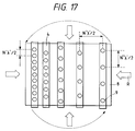
- FIG. 17 is a diagram explanatory of a light direction detector according to the present invention;
- FIGS. 18a and 18b are diagrams explanatory of an optical computer according to the present invention;
- FIG. 19 is a diagram showing sectional structure of a diode including a nanowhisker having a hetero junction;
- FIG. 20 is a diagram explanatory of a structure of a laser having a plurality of nanowhiskers arranged on a regular-triangular substrate;
- FIG. 21 is a diagram showing a structure of a waveguide type laser of the present invention;
- FIG. 22 is a diagram showing an example of a micro-cavity used in the present invention;
- FIG. 23 is a diagram showing a device in which micro-cavity is buried in the core of an optical fiber;
- FIG. 24 is a diagram explanatory of ultra microcrystal growth;
- FIG. 25 is a diagram showing a nanowhisker whose diameter varies periodically in the longitudinal direction;
- FIGS. 26a, 26b, and 26c are diagrams showing a method manufacturing a micro-cavity laser according to the present invention;
- FIG. 27 is a diagram showing a laser formed by burying a micro-cavity in the core of an optical fiber;
- FIG. 28 is a diagram showing a rod type laser of the present invention;
- FIG. 29 is a diagram showing a multi-rod type laser of the present invention;
- FIG. 30 is a sectional view of a light-emitting device having a nanowhisker of the present invention; and
- FIGS. 31 and 32 are graphs showing characteristics of light-emitting devices of the present invention.
- Nanowhiskers were selectively grown on the plane of GaAs (111) B substrate by low-pressure metal organic vapor phase epitaxy and, thereby, a light-emitting rod was produced. In order to grow the nanowhiskers at desired positions, focused ion beams (FIB) were thrown on specified positions of the GaAs (111)
B substrate 3 doped with 10¹⁸/cm³ of a donor as shown in FIG. 2a and, thereby, seeds from which GaAs nanowhiskers would grow were produced. More specifically, the metal forming eutectic with the semiconductor was implanted by FIB and the seeds from which crystals would grow were produced. - Then, nanowhiskers 9 were grown above the portions of the seeds as shown in FIG. 2b by low-pressure metal organic vapor phase epitaxy. Doping of the nanowhisker with impurities was performed such that, first, the nanowhisker was doped with an n-type impurity until it grew to a length of 2.1 µm and, then, the impurity was changed to a p-type impurity and therefrom the nanowhisker of p-type was allowed to grow another length of 2.1 µm. Accordingly, the nanowhisker is 4.2 µm long and has a pn junction formed just in its center. The doping concentration was set to 10¹⁸/cm³ for both the donor and the acceptor.
- Spin-on-glass (SOG) was applied to the substrate with the nanowhiskers grown thereon as shown in FIG. 2c. After the application, the SOG was cured by being held in a temperature of 480°C for 30 minutes and, thereby, an
SOG film 6 being 4 µm thick was formed. The SOG stuck to the tip portion of thenanowhisker 9 was etched along a length of 0.2 µm by a hydrofluoric acid-system etchant and, thereby, the surface of the tip portion was exposed. A p-electrode 4 of a gold-zinc alloy film was formed above the tip portions by evaporation deposition and an ohmic contact was formed thereon by annealing the substrate under a temperature of 450°C. - The rear side of the
substrate 3 was polished by fine polishing powder as shown in FIG. 3a, whereby total thickness was made to 100 µm. A gold-germanium-nickel film was deposited by evaporation on the rear surface of thesubstrate 3 to form an n-electrode 5. The substrate was then annealed under a temperature of 450°C and a laser oscillator as shown in FIG. 1 was produced. An electric field was applied to the laser oscillator and its characteristics were investigated. The laser oscillator shown in FIG. 1 was obtained by linearly arranging the nanowhiskers obtained as described above. It was investigated under what conditions the oscillator can lase. The relationship between the length of the substrate with the nanowhiskers one-dimensionally arranged thereon and the intensity of the oscillated laser beam (normalized power) P/P₀ is shown in FIG. 8b. It was observed, as shown in FIG. 8b, the intensity of the oscillated laser beam sharply increased when the substrate length W exceeded approximately 20 cm. Further, representing the distance between adjoining nanowhiskers by L and the average thickness of the nanowhisker by W, the relationship between L and W at the time when lasing occurred was obtained as shown in FIG. 8a. - In the present embodiment, completely the same results were obtained even if the positions of the p-type region and n-type region were reversed.
- The optical device as shown in the
embodiment 1 was produced not using FIB but through the following process. - First, as shown in FIG. 4, an SiO₂ film 10' was formed on a
GaAs substrate 3 by a thermal CVD method to thickness of 0.1 µm. Then, holes 7 being 0.1 µm in diameter were made in the SiO₂ film 10' by photolithography and vapor phase etching. The distance L between adjoiningholes 7 was set to an integer multiple of semi-wavelength (λ/2). Above theholes 7, n-doped GaAs nanowhiskers were grown by an MOCVD method. Thereafter, the p-electrode and n-electrode were formed in the same way as in theembodiment 1. The micro-cavity laser formed through this process exhibited similar characteristics to those of the laser in theembodiment 1. - Setting the distance between the nanowhiskers L = 172 nm, the thickness of the nanowhisker W = 100 nm, the refractive index of the SOG n₀ = 1, the refractive index of the nanowhisker n₁ = 3.61, the spatial mean value of the refractive index

- In the
embodiments nanowhiskers 9 were arranged on the plane of the n-type GaAs (111)B substrate 3 so that the distance between adjoiningnanowhiskers 9 would become an integer times as large as λ/n₂ as shown in FIG. 10 and SOG was applied onto the same. Then, p-electrodes 4 were formed by evaporation along the rows or columns as shown in FIG. 11. Thereby, it became possible to cause only desired one row or one column of thenanowhiskers 9 to emit light. Further, by applying power only to one row or one column, an extremely narrow laser beam, whose width is comparable to the wavelength of the laser beam, could be obtained. The oscillated laser beams were observed only in the directions indicated by the arrows A in FIG. 10 and not observed in other directions because of attenuation due to interference of light. - In the present embodiment, completely the same results were obtained even if the positions of the p-type region and n-type region were reversed.
- In the
embodiments nanowhiskers 9 were arranged on the plane of a GaAs (111)B semi-insulating substrate 8 so that the distance between adjoiningnanowhiskers 9 would become an integer times as large as λ/n₂ as shown in FIG. 10 and then, before SOG was applied onto thesubstrate 8 with thenanowhiskers 9 formed thereon, n-electrodes 5 were formed as shown in FIG. 5a. When gold, germanium, and nickel were evaporated for forming the n-electrodes 5, the quantity of the gold, germanium, and nickel sticking to thenanowhisker 9 was small because the direction of flying atoms during the evaporation deposition and the direction of thenanowhisker 9 are opposite to each other, and so they could be easily removed by etching. Then, SOG was applied and baked in the same way as in theembodiments embodiment 3. Thereby, it became possible to cause only desired one row or one column of the nanowhiskers to emit light. Further, by applying power only to one row or one column of the nanowhiskers, an extremely narrow laser beam, whose width is comparable to the wavelength of the laser beam, could be obtained. The oscillated laser beams were observed only in the directions indicated by the arrows A in FIG. 10 and not observed in other directions because of attenuation due to interference of light. - In the present embodiment, completely the same results were obtained even if the positions of the p-type region and n-type region were reversed.
- In the
embodiments nanowhiskers 9 were arranged on the plane of a GaAs (111)B semi-insulating substrate 8 so that the distance between adjoiningnanowhiskers 9 would become an integer times as large as λ/n₂ as shown in FIG. 10. Then, n-electrodes 5 were formed on thesubstrate 8 in an array of rows or columns as shown in FIG. 5a and FIG. 12. The electrode material stuck to thenanowhisker 9 was easily removed by etching the same as in theembodiment 4. Then,SOG 6 was applied and baked and, then, p-electrodes 4 were formed in the same way as in theembodiment 2. Thus, it became possible to cause one of the nanowhiskers to emit light by applying power to the p-electrode 4 connected to the desirednanowhisker 9 of the described arrangement. - It is of course possible to cause a plurality of desired
nanowhiskers 9 to emit light. - In the present embodiment, completely the same results were obtained even if the positions of the p-type region and n-type region were reversed.
- A plurality of
nanowhiskers 9 were formed on the plane of a GaAs (111)B semi-insulating substrate 8 so that the distance between adjoiningnanowhiskers 9 would become an integer times as large as λ/n₂ as shown in FIG. 13 and, then, electrodes were formed in the same way as in theembodiment 4. Laser beams were lased only in the directions as indicated by the arrows A in FIG. 13. - In the present embodiment, completely the same results were obtained even if the positions of the p-type region and n-type region were reversed.
- In the same way as in the
embodiment 5, a plurality of nanowhiskers were formed on the plane of a GaAs (111)B semi-insulating substrate 8 so that the distance between adjoiningnanowhiskers 9 would become an integer times as large as λ/n₂ as shown in FIG. 14 and, then, electrodes were formed in the same way as in theembodiment 4. Laser beams were lased only in the directions as indicated by the arrows A in FIG. 14. - In the present embodiment, completely the same results were obtained even if the positions of the p-type region and n-type region were reversed.
- A plurality of
nanowhiskers 9 were formed on the plane of a GaAs (111)B semi-insulating substrate 8 so that the distance between adjoiningnanowhiskers 9 in one direction would become an integer times as large as λ/n₂ and the distance in the other direction would become half the above value as shown in FIG. 9 and, then, electrodes were formed in the same way as in theembodiment 4. Laser beams were lased only in the directions as indicated by the arrows A in FIG. 9. - In the present embodiment, completely the same results were obtained even if the positions of the p-type region and n-type region were reversed.
- An optical device was produced through the same process as that for the
embodiment 5. However, a transparent electrode formed of an SnO₂ film was used as the p-electrode 4 on the top surface of the device. The distance L between adjoiningnanowhiskers 9 was set to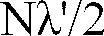
- In the present embodiment, completely the same results were obtained even if the positions of the p-type region and n-type region were reversed.
- An apparatus as shown in FIG. 16b was structured using the optical device produced by the method shown in the
embodiment 2. A high voltage (1.5 V) was applied to this apparatus and a laser beam with a wavelength of around 860 nm lased from another semiconductor laser was transmitted through the apparatus. The laser beam R then emitted was better in coherence than the beam introduced therein. By arranging as described above, the optical device according to the present invention can be used not only as an oscillator but also as a resonator of laser beam. - Further, when, while a high voltage (1.5 V) was applied to the apparatus structured in the
embodiment 9, a laser beam from another semiconductor laser was introduced into the apparatus as shown in FIG. 16b, a beam with extremely good coherence was emitted deflected in the vertical direction. - In the present embodiment, completely the same results were obtained even if the polarities p and n were reversed.
- Structuring the apparatus shown in FIG. 16b in the same way as described in the
embodiment 10, an electric measuring instrument was connected to the optical device instead of the voltage source having been connected to the same. Then, it was observed that a voltage of 1.5 V was impressed on the instrument. When the beam from the semiconductor laser was modified to a pulse signal, the optical device could accurately convert the light signal into an electric signal. - Further, when the distance between adjoining
nanowhiskers 9 was changed in various ways as shown in FIG. 16c, the incoming light pulse signal was correctly read by the optical device even if the incoming laser beam was changed variously. - Further, when the distance between the
nanowhiskers 9 was changed for each row or column andelectrodes 4 were formed as shown in FIG. 17, the optical devices read signals of electromagnetic wave transmitted from the surroundings and indicated the transmitted directions and power of the signals as electric signals. - Even if the positions of the p-type region and n-type region are reversed in the present embodiment, the device is equally usable though only the polarities of the electric characteristics are reversed.
- This embodiment will be described with reference to FIG. 19. GaAs/AlGaAs hetero nanowhiskers were formed by an MOCVD method on an n-type GaAs (111)
substrate 101 doped with Si in a density of 10¹⁹/cm³. First, Ga ions were implanted into specified regions in thesubstrate 101 by a focused ion beam method. As crystals are allowed to grow, the crystal growth selectively occurs only at the portion where the Ga ions were implanted. This phenomenon was utilized for producing nanowhiskers. The diameter of the Ga ion beam was set to 20nm so that the thickness of the crystal growing above it may become 20nm measured immediately above the substrate. First, an n-type AlGaAs crystal 102 doped with Si in a density of 10¹⁹/cm³ was grown. Then, an i-type GaAs crystal 103 doped with no impurity was grown. Further, a p-type AlGaAs crystal 104 doped with Zn in a density of 10¹⁹/cm³ was grown. Al content in the AlGaAs crystal was 0.1. The crystal growing times were set so that the lengths of the n-type and p-type AlGaAs crystals type GaAs crystal 103 was set to 30nm. - Then, for stabilization of the surface of the nanowhisker, an AlGaAs layer of which Al content was 0.2 was grown as a
cap layer 105 to a thickness of 200 nm. Since the Al content of thecap layer 105 is higher than that of the nanowhisker portion, the current injected into the nanowhisker does not flow into thecap layer 105. As thecap layer 105, not only the AlGaAs layer but also a transparent insulating member such as an SiO₂ film or an SOG resin with a thickness of 200 nm can be used. At this time, before depositing thecap layer 105, the surface of the nanowhisker was dipped in a water solution of NH₄S₂, Li₂S for 20 to 30 hours and, then, heated at a temperature of 50°C. Thereafter, the substrate was heated in hydrogen gas at a temperature of 390°C for 30 minutes. By this treatment, an oxide film on the surface of the nanowhisker is reduced and a good surface in which non-radiative electron-hole recombination is reduced can be obtained. - The electrode for current injection was formed as follows. Au was deposited by evaporation on the rear surface of the
substrate 101 to a thickness of 100 nm to thereby form agrounding electrode 107. Au/Zn alloy was deposited by evaporation on the surface of thecap layer 105 to a thickness of 100 nm and, thereby, the electrode forcurrent injection 106 was formed. A forward voltage is applied to the pn junction within the nanowhisker through theelectrode 106 and, thereby, the current injection can be achieved. - In the present embodiment, a method for producing a nanowhisker having a pin junction in a hetero structure was described. It is possible to have an array of nanowhiskers well suited for use as a laser by controlling positions where focused ion beams are implanted, which will be described later in another embodiment. The nanowhisker having the hetero pin junction produced in the present embodiment can provide higher light-emitting efficiency than other nanowhiskers and the threshold current density can be reduced when a laser is formed of the same. Although an n-type substrate was used in the present embodiment described above, a hetero pin junction can be formed by a similar method even if a p-type substrate is used. As the method for selectively growing nanowhiskers, not only the method using the focused ion beam method but also the method using a mask pattern formed of an insulating film can be used. That is, first, an SiO₂ film is formed on a substrate by the known sputtering method to a thickness of 50 nm and, then, a resist is applied onto the same and holes whose diameter is 20 nm are made therein by electron beam exposure, and then, nanowhiskers are grown at the hollowed portions. Thus, the positions where nanowhiskers grow can be specified.
- In the present embodiment, an example in which device was structured using GaAs and AlGaAs was shown. Similar device can also be produced by using, as the substrate and the p-i-n portion, GaAs and GaAs-InAs-GaAs, or InP and InP-InGaAsP-InP, respectively.
- An array of nanowhiskers formed by the method described in the embodiment 12 for structuring a laser will now be described. Since the (111) plane is used as the substrate plane, the
substrate 3 can be cleaved into regular triangular form as shown in FIG. 20. The cleavage surfaces corresponding to the sides of the regular triangle will be denoted by X, Y, and Z. The array of thenanowhiskers 108 and treatment of the cleavage surfaces depend on the manner how the laser beam is taken out. The array of thenanowhiskers 108 is decided by setting the positions, where the focused ion beams mentioned in the embodiment 12 are implanted, as shown in FIG. 20. When a laser beam is taken out from one surface in the direction perpendicular to the surface, assuming the surface to be X, it may be well to set L1 to an integer multiple of the oscillation wavelength and L2 to another value than that. At this time,nonreflective coatings 


- An example of waveguide type laser using a nanowhisker is shown in this embodiment. Nanowhiskers are formed by the method shown in the embodiments 12 and 13. However, the cleaving of the substrate is not yet done at this stage. A resist is applied onto a
current injection electrode 106 described in the embodiment 12, the substrate is heated and an optical waveguide pattern of a transmission line form is formed by contact mask exposure, and chemical etching is performed using the pattern and, thereby, an opticalwaveguide type laser 113 is produced. Then, the substrate is cleaved and asubstrate 112 and alaser waveguide 113 as shown in FIG. 21 are obtained. The arrangement of nanowhiskers in thelaser waveguide 113 is set to be corresponding to the arrangement given first in the embodiment 13. Finally, the end face of the waveguide is covered by anonreflective coating film 114. - A micro-cavity laser as shown in FIG. 22 was produced. First, ultra microcrystals 205 were grown by selective growth method on a GaAs (111)
B semi-insulating substrate 204 as shown in FIG. 26a. More specifically, anSiO₂ film 206 being 0.6 µm thick was formed on theGaAs substrate 204 by a thermal CVD method. Then, a plurality of holes whose diameter is 20 µM were made in theSiO₂ film 206 by the known photolithographic technique. On thesubstrate 204 having thereon the SiO₂ film with the holes, n-dopedGaAs microcrystals 205 were grown by a metal organic chemical vapor deposition method (MOCVD method). The form of the crystal can be controlled by the growing conditions. Since the crystal has the property growing in the (111) direction, when the (111)B substrate 204 is used as in the present embodiment, the crystal grows in the direction perpendicular to thesubstrate 204 as shown in FIG. 26a. In the present embodiment, the growing conditions were set such that the substrate temperature was 480°C, the ratio between material gases of the V group and IV group (i.e., AsH₃ and trimethyl aluminum, respectively) was V/III = 20, and the growing time was 20 minutes. The microcrystal grown at this time was approximately 3 µm long. Then, above the n-GaAs microcrystal, a p-GaAs microcrystal was successively grown under the same conditions as those used for growing the n-GaAs microcrystal. The growing time was similarly set to 20 minutes. As a result, themicrocrystal 205 totally 6 µm long was formed. As dopant, monosilane for doping with Si was used when forming the n-GaAs microcrystal and obtained the n-GaAs microcrystal whose carrier density = 1 x 10¹⁸/cm³. On the other hand, when forming the p-GaAs microcrystal, biscyclopentadiethylmagnesium was used and the p-GaAs microcrystal whose carrier density = 2 x 10¹⁸/cm³ was obtained. The grownmicrocrystals 205 were buried in aresin 207 as shown in FIG. 26a, and then, themicrocrystals 205, together with theresin film 207, were taken out from thesubstrate 209, and then both sides of theresin film 207 were polished by very fine polishing agent so that a form with a thickness of 4 µm as shown in FIG. 26c was obtained. Then,transparent SnO₂ films 208 were formed on both sides and thereby a micro-cavity laser was produced. By passing electric current through the thus obtained micro-cavity laser to allow it to lase, a low-threshold value laser was obtained, of which the threshold current value for lasing is as low as 1 µA. - A micro-cavity laser having a structure as shown in FIG. 25 was produced. The method for manufacturing it is the same as that shown in the embodiment 16, but modulation growing was performed in this case in order to periodically vary the diameter in the longitudinal direction. More specifically, the ratio between V group dopant and III group dopant (V/III ratio) during the time of crystal growth was alternately changed between 18 and 22 every five minutes.
- The threshold current value for lasing the thus obtained micro-cavity laser was as low as 1 µA the same as in the embodiment 15, and the laser beam lased by the same, with the half-width being 1 MHz, was very good in coherence.
- An arrangement of a
micro-cavity laser 201 buried in thecore 202 of anoptical fiber 203 as shown in FIG. 23 was produced. By producing micro-cavity lasers by the method shown in the embodiment 14, one of them was taken out and buried into thecore 202 of a quartzoptical fiber 203. In order to pass current through the micro-cavity laser, minute holes were made in theoptical fiber 203 sideways and leadwires 209 were taken out as shown in FIG. 27. In the case of a micro-cavity laser of the described arrangement, its coupling efficiency with the optical fiber was very high as 90%. - By periodically changing the contents of crystal, a micro-cavity laser similar to the embodiment 16 was produced. As shown in FIG. 28, 50 layers of n-
type GaAs 302 and n-type GaAlAs 303 were alternately piled up in the longitudinal direction on aGaAs substrate 301, then, above the same, an n-type Al0.5Ga0.5Aslayer 304, an In0.2Ga0.8Aslayer 305 including virtually no impurity, and a p-type Al0.5Ga0.5Aslayer 306 were piled, and further, above the same, 50 layers of p-type GaAs 308 and p-type GaAlAs 307 were alternately piled up, and thereby a semiconductor rod is formed. At this time, the film thickness of the n-type GaAs 302 and n-type GaAlAs 303 as well as the p-type GaAs 308 and p-type GaAlAs 307 were all set to a quarter of the emission wavelength. - Electrodes (not shown) were provided at the top and bottom of the micro-cavity formed as described above. When current was passed through the electrodes longitudinally in the forward direction of the pn junction, a laser beam having good coherence similarly to that in the embodiment 16 was obtained.
- N-type GaAlAs was grown 1 µm in the longitudinal direction, and then, above the same, a GaAs layer including virtually no impurity was grown to a thickness of 2 nm, and, further, above the same, p-type GaAlAs was grown 1 µm, and, thereby, a plurality of semiconductor rods were formed. These semiconductor rods were arranged in an area of 2 µm square at a distance virtually equal to the diameter of the rod. Electrodes were provided at the top and bottom of the rods in order to pass current in the longitudinal direction. When a current was passed in the forward direction of the pn junction, a laser beam having very good coherence similarly to that in the embodiment 16 was obtained.
- FIG. 30 shows a schematic sectional view of a pn junction light-emitting device whose crystal surface was treated by sulfur (S) or selenium (Se) for its stabilization. In the diagram,
reference numeral 401 denotes an n-type InP substrate, and 402 and 403 denote portions where a nanowhisker was formed.Reference numeral 404 denotes the treated layer for surface stabilization formed on the outer surface of the nanowhisker through the above described treatment with S or Se.Reference numeral type region 406 is 1 µm long, the p-type region 408 is 1 µm long, and theundoped region 407 is 10 nm long. Further, 409 and 410 denote electrodes. When theelectrode 409 is supplied with a positive bias and theelectrode 410 is supplied with a negative bias, a current flows in the direction indicated by thearrow 411. The thickness of thecurrent transmission line 402 of the nanowhisker is indicated by D₂ and the thickness of the nanowhisker including itssurface depleion layer 403 is indicated by D₁. In the present embodiment, D₁ is 20 nm and D₂ is 15 nm. When the surface stabilization treatment with S or Se is performed, the thickness of thesurface depletion layer 403 is reduced by 20 to 60% due to the existence of the treatedlayer 404 for surface stabilization. Accordingly, the thickness D₂ of thecurrent transmission line 402 of the nanowhisker is increased by 10 to 20% and, hence, it becomes 16 to 18 nm. When a current 411 was passed, light emitted from the portion with theundoped region 407 in the center was observed. - A graph of relationship between emission gain of the light-emitting device and the emission wavelength is shown in FIG. 31. Referring to FIG. 31, the curves a and b show the case where the surface stabilization treatment of the nanowhisker was performed and the case where the stabilization treatment was not performed, respectively. As apparent from FIG. 32, the working time is extremely prolonged by performing the surface stabilization treatment. Further, as is known from the curve a of FIG. 31, the emission wavelength is shifted to the longer wavelength side by 0.05 µm or so from that of the curve b for the case where the surface stabilization treatment was not performed. The reason why the emission wavelength is shifted to the longer wavelength side when the surface stabilization treatment is performed is because the thickness of the depletion layer on the crystal surface is reduced and the width of the current transmission line where carriers are kept in is increased. On the other hand, the gain increased 1.5 to 2 times. This is because the rate of non-radiative recombination was reduced by the stabilization of the crystal surface.
- FIG. 32 shows dependence on working time of relative emission intensity in the present embodiment. The graph is the results of investigation of aged change of the peak emission intensity of the light-emitting device. In the case where the surface stabilization treatment was not performed, as apparent from the curve, the peak emission intensity gradually decreased with the working time in the range from 103 hours to 10⁴ hours and it sharply decreased after 10⁴ hours passed. On the other hand, in the case where the surface stabilization treatment was performed, as shown by the curve a, the peak emission intensity showed little change even in the range from 10⁴ to 10⁵ hours. Thus, it was observed that the life span of the light-emitting device was prolonged more than 10 times by the surface stabilization treatment.
- According to the present invention as described in the foregoing, a semiconductor laser can be realized by disposing semiconductor rods having a pn junction or a hetero junction at intervals of an integer multiple of the oscillation frequency and an optical antenna can be produced using the same apparatus.
- Further, according to the present invention, a micro-cavity laser whose threshold current is extremely small, as well as a coherent light-emitting device and coherent LED having no threshold value, can be formed, and therefore, key devices very effective for use in the field of optical communications can be obtained. This is because only a limited number of modes can contribute to lasing in the micro-cavity. Further, since the micro-cavity laser according to the present invention can be buried into the core of an optical fiber, it provides such a merit that the coupling efficiency between the optical fiber and the laser is greatly increased. Thus, great industrial advantages can be obtained from the present invention.
Claims (18)
- A semiconductor optical device comprising:
a semiconductor substrate (3),
a plurality of semiconductor rods (9), each having a pn junction, formed on a main surface of said substrate (3) in a direction substantially perpendicular to said main surface, and
electrodes(4, 5) connected with the p-type regions and n-type regions of said rods (9), wherein
at least a portion of said plurality of rods (9) are arranged at substantially equal distances. - The device of claim 1, wherein a portion of said plurality of rods (9) are arranged at a first distance and the remainder of said rods are arranged at second distance which is different from the first distance.
- The device of claim 1 or 2, wherein said rods (9) are single-crystalline nanowhiskers grown on the surface of said substrate (3) by epitaxial growth.
- The device of any of claims 1 to 3, wherein the diameter of said rod (9) periodically changes according to the position along its length.
- The device of any of claims 1 to 4, wherein the distance between adjacent rods (9) is equal to an integer multiple of the wavelength of light emitted from said rod.
- The device of claim 5, wherein the distance between adjacent rods (9) is substantially different from the wavelength of second light emitted in a direction different from the direction of said light.
- The optical device of any of claims 1 to 6, wherein an i-type region (103) is sandwiched between the p-type region (104) and n-type region (102) of said rod.
- The device of any of claims 1 to 7, wherein said rod (9) is formed of the same material as said substrate (3).
- The device of claim 8, wherein said material is GaAs.
- The device of any of claims 1 to 7, wherein said substrate 3 and said rod (9) are formed of different materials.
- The device of claim 10, wherein said substrate is formed of GaAs and said rod includes GaAlAs.
- The device of claim 11, wherein said rod further includes InGaAs.
- The device of claim 10, wherein said substrate is formed of InP and said rod includes InGaAs.
- The device of any of claims 1 to 3, wherein the diameter of said rod on said substrate is not larger than 1,000 nm.
- The device of any of claims 1 to 14, wherein the crystalline orientation of said rod in the longitudinal direction is (111).
- The device of any of claims 1 to 15, wherein said plurality of rods are arranged one-dimensionally on the surface of said substrate.
- The device of any of claims 1 to 15, wherein said plurality of rods are arranged two-dimensionally on the surface of said substrate (3).
- The device of claim 17, wherein said plurality of rods (9) are arranged in a regular polygon configuration on the surface of said substrate (3).
Applications Claiming Priority (2)
| Application Number | Priority Date | Filing Date | Title |
|---|---|---|---|
| JP58570/91 | 1991-03-22 | ||
| JP5857091A JP3181303B2 (en) | 1990-04-20 | 1991-03-22 | Light emitting element |
Publications (3)
| Publication Number | Publication Date |
|---|---|
| EP0504851A2 true EP0504851A2 (en) | 1992-09-23 |
| EP0504851A3 EP0504851A3 (en) | 1993-02-03 |
| EP0504851B1 EP0504851B1 (en) | 1997-07-16 |
Family
ID=13088101
Family Applications (1)
| Application Number | Title | Priority Date | Filing Date |
|---|---|---|---|
| EP92104703A Expired - Lifetime EP0504851B1 (en) | 1991-03-22 | 1992-03-18 | Semiconductor optical device |
Country Status (2)
| Country | Link |
|---|---|
| EP (1) | EP0504851B1 (en) |
| DE (1) | DE69220824T2 (en) |
Cited By (1)
| Publication number | Priority date | Publication date | Assignee | Title |
|---|---|---|---|---|
| EP2333847A4 (en) * | 2008-09-01 | 2015-02-25 | Sophia School Corp | OPTICAL SEMICONDUCTOR ELEMENT ASSEMBLY AND METHOD OF MANUFACTURING THEREOF |
Family Cites Families (2)
| Publication number | Priority date | Publication date | Assignee | Title |
|---|---|---|---|---|
| JPH01319985A (en) * | 1988-06-21 | 1989-12-26 | Matsushita Electric Ind Co Ltd | Method and device for manufacture compound semiconductor quantum box and treating method for ultrafine particle and light-emitting device |
| US5362972A (en) * | 1990-04-20 | 1994-11-08 | Hitachi, Ltd. | Semiconductor device using whiskers |
-
1992
- 1992-03-18 DE DE69220824T patent/DE69220824T2/en not_active Expired - Fee Related
- 1992-03-18 EP EP92104703A patent/EP0504851B1/en not_active Expired - Lifetime
Cited By (2)
| Publication number | Priority date | Publication date | Assignee | Title |
|---|---|---|---|---|
| EP2333847A4 (en) * | 2008-09-01 | 2015-02-25 | Sophia School Corp | OPTICAL SEMICONDUCTOR ELEMENT ASSEMBLY AND METHOD OF MANUFACTURING THEREOF |
| US9224595B2 (en) | 2008-09-01 | 2015-12-29 | Sophia School Corporation | Semiconductor optical element array and method of manufacturing the same |
Also Published As
| Publication number | Publication date |
|---|---|
| DE69220824T2 (en) | 1998-01-29 |
| EP0504851B1 (en) | 1997-07-16 |
| DE69220824D1 (en) | 1997-08-21 |
| EP0504851A3 (en) | 1993-02-03 |
Similar Documents
| Publication | Publication Date | Title |
|---|---|---|
| US5332910A (en) | Semiconductor optical device with nanowhiskers | |
| JP4138930B2 (en) | Quantum semiconductor device and quantum semiconductor light emitting device | |
| JP2984365B2 (en) | Distributed feedback laser | |
| US20060071218A1 (en) | Semiconductior multilayer structurehaving inhomogeneous quantum dots, light-emitting diode using same, semiconductor laser diode, semiconductor optical amplifier, and method for manufacturing them | |
| US4212020A (en) | Solid state electro-optical devices on a semi-insulating substrate | |
| US6031859A (en) | Mode-locked semiconductor laser | |
| KR940005764B1 (en) | Laser diode array and its manufacturing method | |
| US4270096A (en) | Semiconductor laser device | |
| JP3181303B2 (en) | Light emitting element | |
| JP2867819B2 (en) | Multiple quantum well semiconductor laser | |
| US4352116A (en) | Solid state electro-optical devices on a semi-insulating substrate | |
| US5852625A (en) | Distributed feedback semiconductor laser | |
| Razeghi et al. | cw operation of 1.57‐μm Ga x In1− x As y P1− y InP distributed feedback lasers grown by low‐pressure metalorganic chemical vapor deposition | |
| EP1354380A2 (en) | Quantum dot lasers | |
| US7184640B2 (en) | Buried heterostructure device fabricated by single step MOCVD | |
| US4833684A (en) | Distributed feedback laser with anti-reflection layer | |
| EP0504851B1 (en) | Semiconductor optical device | |
| US4813049A (en) | Semimagnetic semiconductor laser | |
| CN112736645B (en) | Preparation method of gain medium of high-power semiconductor optical amplifier | |
| JP2004342851A (en) | Method for growing semiconductor film and semiconductor device provided with this semiconductor film | |
| Nordell et al. | MOVPE regrowth of semi-insulating InP around reactive ion etched laser mesas | |
| Arai et al. | Growth of highly strained GaInAs-GaAs quantum wells on patterned substrate and its application for multiple-wavelength vertical-cavity surface-emitting laser array | |
| KR0144490B1 (en) | Manufacturing method of semiconductor laser diode | |
| KR900008625B1 (en) | Manufacturing method of laser-diode using phase fixotion | |
| KR100278630B1 (en) | Semiconductor laser diode and manufacturing method thereof |
Legal Events
| Date | Code | Title | Description |
|---|---|---|---|
| PUAI | Public reference made under article 153(3) epc to a published international application that has entered the european phase |
Free format text: ORIGINAL CODE: 0009012 |
|
| AK | Designated contracting states |
Kind code of ref document: A2 Designated state(s): DE FR GB NL |
|
| PUAL | Search report despatched |
Free format text: ORIGINAL CODE: 0009013 |
|
| AK | Designated contracting states |
Kind code of ref document: A3 Designated state(s): DE FR GB NL |
|
| 17P | Request for examination filed |
Effective date: 19930714 |
|
| 17Q | First examination report despatched |
Effective date: 19931027 |
|
| GRAG | Despatch of communication of intention to grant |
Free format text: ORIGINAL CODE: EPIDOS AGRA |
|
| GRAH | Despatch of communication of intention to grant a patent |
Free format text: ORIGINAL CODE: EPIDOS IGRA |
|
| GRAH | Despatch of communication of intention to grant a patent |
Free format text: ORIGINAL CODE: EPIDOS IGRA |
|
| GRAA | (expected) grant |
Free format text: ORIGINAL CODE: 0009210 |
|
| AK | Designated contracting states |
Kind code of ref document: B1 Designated state(s): DE FR GB NL |
|
| PG25 | Lapsed in a contracting state [announced via postgrant information from national office to epo] |
Ref country code: FR Effective date: 19970716 |
|
| REF | Corresponds to: |
Ref document number: 69220824 Country of ref document: DE Date of ref document: 19970821 |
|
| EN | Fr: translation not filed | ||
| PLBE | No opposition filed within time limit |
Free format text: ORIGINAL CODE: 0009261 |
|
| STAA | Information on the status of an ep patent application or granted ep patent |
Free format text: STATUS: NO OPPOSITION FILED WITHIN TIME LIMIT |
|
| 26N | No opposition filed | ||
| REG | Reference to a national code |
Ref country code: GB Ref legal event code: IF02 |
|
| PGFP | Annual fee paid to national office [announced via postgrant information from national office to epo] |
Ref country code: GB Payment date: 20020301 Year of fee payment: 11 |
|
| PGFP | Annual fee paid to national office [announced via postgrant information from national office to epo] |
Ref country code: NL Payment date: 20020306 Year of fee payment: 11 |
|
| PGFP | Annual fee paid to national office [announced via postgrant information from national office to epo] |
Ref country code: DE Payment date: 20020328 Year of fee payment: 11 |
|
| PG25 | Lapsed in a contracting state [announced via postgrant information from national office to epo] |
Ref country code: GB Free format text: LAPSE BECAUSE OF NON-PAYMENT OF DUE FEES Effective date: 20030318 |
|
| PG25 | Lapsed in a contracting state [announced via postgrant information from national office to epo] |
Ref country code: NL Free format text: LAPSE BECAUSE OF NON-PAYMENT OF DUE FEES Effective date: 20031001 Ref country code: DE Free format text: LAPSE BECAUSE OF NON-PAYMENT OF DUE FEES Effective date: 20031001 |
|
| GBPC | Gb: european patent ceased through non-payment of renewal fee |
Effective date: 20030318 |
|
| NLV4 | Nl: lapsed or anulled due to non-payment of the annual fee |
Effective date: 20031001 |