EP0504842B1 - Array antenna - Google Patents
Array antenna Download PDFInfo
- Publication number
- EP0504842B1 EP0504842B1 EP92104692A EP92104692A EP0504842B1 EP 0504842 B1 EP0504842 B1 EP 0504842B1 EP 92104692 A EP92104692 A EP 92104692A EP 92104692 A EP92104692 A EP 92104692A EP 0504842 B1 EP0504842 B1 EP 0504842B1
- Authority
- EP
- European Patent Office
- Prior art keywords
- low noise
- feeder circuit
- array antenna
- noise amplifiers
- overlaid
- Prior art date
- Legal status (The legal status is an assumption and is not a legal conclusion. Google has not performed a legal analysis and makes no representation as to the accuracy of the status listed.)
- Expired - Lifetime
Links
Images




Classifications
-
- H—ELECTRICITY
- H01—ELECTRIC ELEMENTS
- H01Q—ANTENNAS, i.e. RADIO AERIALS
- H01Q1/00—Details of, or arrangements associated with, antennas
- H01Q1/36—Structural form of radiating elements, e.g. cone, spiral, umbrella; Particular materials used therewith
- H01Q1/38—Structural form of radiating elements, e.g. cone, spiral, umbrella; Particular materials used therewith formed by a conductive layer on an insulating support
-
- H—ELECTRICITY
- H01—ELECTRIC ELEMENTS
- H01Q—ANTENNAS, i.e. RADIO AERIALS
- H01Q21/00—Antenna arrays or systems
- H01Q21/06—Arrays of individually energised antenna units similarly polarised and spaced apart
- H01Q21/061—Two dimensional planar arrays
-
- H—ELECTRICITY
- H01—ELECTRIC ELEMENTS
- H01Q—ANTENNAS, i.e. RADIO AERIALS
- H01Q23/00—Antennas with active circuits or circuit elements integrated within them or attached to them
Definitions
- the present invention relates to an array antenna for receiving signals in a microwave region.
- Figure 5 is a diagram showing a conventional radiowave receiving array antenna wherein reference numeral 1 designates a lower earthing conductor, numeral 2 designates a feeder circuit board, numeral 3 designates an upper earthing conductor, numerals 4 designate supporting plates, numerals 5 designate low noise amplifiers, numerals 6 designate power source lines for the low noise amplifiers, numeral 7 designates a number of radiation elements, numeral 8 designates a feeder circuit, numerals 9 designate a metal pins and numeral 10 designates a number of radiation windows.
- radiowaves received by the radiation elements 7 in the feeder circuit board are synthesized by the feeder circuit 2, the synthesized signal is amplified by the low noise amplifiers 5, and then, is supplied to a receiver.
- the feeder circuit 2 a loss of electric energy produces noises, whereby the quality of an electric signal is deteriorated.
- the a level of deterioration exceeds an allowable range, it is necessary to divide the antenna into sub-arrays and to insert the low noise amplifiers 5 in each sub-array.
- influence by a loss produced in the feeder circuit from the low noise amplifiers 5 to the output terminals of the antenna can be reduced in inverse proportion to the gain of the low noise amplifiers 5 by inserting a plurality of low noise amplifiers 5 in the feeder circuit 2.
- the conventional radiowave receiving array antenna having the construction described above had disadvantages as follows.
- the structure for connecting the low noise amplifiers to the feeder circuit is complicated to thereby increase cost.
- the low noise amplifiers are mounted on the back surface of the lower earthing conductor, the thickness of the antenna device is increased.
- a cover for protecting the low noise amplifiers is additionally needed, whereby the construction is further complicated to thereby increase cost.
- EP 0 055 324 A2 discloses a monolithic microwave circuit with array elements, a feed network and low noise amplifiers being integrated on a single substrate of semiconductor material.
- JP 1-114106 A describes a structure in which a portion corresponding to a feeding terminal on the earthing conductor protrudes towards the feed circuit board and an amplifier is attached to the top of the portion.
- JP 1-114104 A and JP 1-114105 A a low noise amplifier is provided in the space between the earthing conductor and the feeder circuit board so as to be perpendicular or parallel to both the earthing conductor and the feeder circuit board, respectively.
- connection of the low noise amplifiers to the feeder circuit can be easy because the low noise amplifiers are mounted on the same plane as the feeder circuit.
- the low noise amplifiers were generally formed on microstrip lines. Insertion of the converting device comprising a rectangular coaxial member between a triplate line and a microstrip line in the feeder circuit assures effective conversion and provides a simple and efficient structure.
- the upper earthing conductor is covered by a radome. Accordingly, the low noise amplifiers can be mounted, without the necessity of an additional protecting means, by arranging the power source lines for the amplifiers on the upper earthing conductor.
- the power source lines for the upper earthing conductor and the low noise amplifiers are formed, by etching or the like, on both surfaces of a double-side-metal-sheet-lined substrate, whereby the number of elements can be reduced so that the manufacturing cost can be reduced.
- reference numeral 1 designates a lower earthing conductor or a lower earthing conductive plate
- numeral 2 designates a feeder circuit board comprising an insulating film on which a feeder circuit is formed
- numeral 3 designates an upper earthing conductor or an upper earthing conductive plate made of a metallic substance
- numerals 4 designate first and second supporting plates made of a foamed resinous material
- numeral 5 designate low noise amplifiers
- numeral 7 designate a number of radiation elements formed on the insulating film which is overlaid on the first supporting plate 4
- numeral 8 designates the feeder circuit
- numeral 10 designate a number of radiation windows formed in the upper earthing conductor 3.
- the feeder circuit board 2 is sandwiched between the first and second supporting plates 4; the upper earthing conductor 3 is overlaid on the other surface of the first supporting plate 4 and the lower earthing conductor 1 is overlaid on the other surface of the second supporting plate 4.
- the low noise amplifiers 5 are mounted on the same plane as the feeder circuit board 2. In comparison with the conventional technique wherein the low noise amplifiers are mounted on the back surface of the lower earthing conductor 1 ( Figure 5), it is unnecessary to provide means for connecting the low noise amplifiers 5 to the feeder circuit 8, on the lower earthing conductor 1. Further, it is unnecessary to provide a cover for protecting the low noise amplifiers 5. In order to mount the low noise amplifiers on the same plane as the feeder circuit board 2, it is necessary to create spaces by sacrificing a part of the radiation elements 7. However, if the number of the radiation elements is sufficiently large, the deterioration of the characteristics of the antenna due to the reduction of the number of the radiation elements is negligible.
- Figure 2 shows another embodiment of the array antenna according to the present invention.
- the same reference numerals as in Figure 1 designate the same element, and therefore, description of these elements is omitted.
- reference numeral 11 designates a rectangular coaxial type inner conductor
- numeral 12 designates a rectangular coaxial type outer conductor
- numeral 13 designates a microstrip line for a low noise amplifier
- numeral 14 designates an earthing conductor for the microstrip line 16.
- the rectangular coaxial type inner and outer conductors 11, 12 constitutes a converting device.
- the insertion of the converting device between the microstrip line and a triplate line suppresses the deterioration of efficiency of transmitting electromagnetic waves.
- the deterioration of the transmission efficiency is caused because the microstrip line forms an imbalance type transmission path and the triplate line forms a balance type transmission path, and therefore, if the both lines are directly connected, imbalanced, undesired electromagnetic waves are produced at the connection area so as to keep the continuity of electric field, to thereby deteriorate the transmission efficiency.
- the rectangular coaxial type converting device forms a balance type transmission path.
- the converting device comprising rectangular coaxial type inner and outer conductors is inserted in a converting section where there are the microstrip line 13 for a low noise amplifier and the triplate line in the feeder circuit 8, wherein the dimension of the longer inner side of the outer conductor is determined to be able to cut off a waveguide mode at an available frequency.
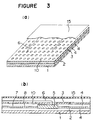
- Figure 3 shows another embodiment of the antenna array according to the present invention.
- the same reference numerals as in Figure 1 designate the same elements except that the array antenna of this embodiment has a radome 15.
- the radome 15 is generally attached to an array antenna for outdoor use. Accordingly, by arranging the power source lines 6 for the low noise amplifiers between the upper earthing conductor 3 and the radome 15, it is unnecessary to provide an additional protecting means for the power source lines 6.
- Figure 4 shows another embodiment of the array antenna according to the present invention.
- the same reference numerals as in Figure 1 designate the same or corresponding elements except that numeral 9 designate metal pins and numeral 16 designates a double-side-metal-sheet-lined substrate.
- the upper earthing conductor 3 and the power source lines 6 are formed, by etching or the like, on both surfaces of a single double-side-metal-sheet-lined substrate, whereby the number of structural elements can be further reduced.
- low noise amplifiers are mounted on the same plane as a feeder circuit, or power source lines are arranged on the upper earthing conductor, whereby the construction of an array antenna can be simplified and the manufacturing cost can be reduced.
Landscapes
- Variable-Direction Aerials And Aerial Arrays (AREA)
- Waveguide Aerials (AREA)
Description
- The present invention relates to an array antenna for receiving signals in a microwave region.
- Figure 5 is a diagram showing a conventional radiowave receiving array antenna wherein
reference numeral 1 designates a lower earthing conductor,numeral 2 designates a feeder circuit board,numeral 3 designates an upper earthing conductor,numerals 4 designate supporting plates,numerals 5 designate low noise amplifiers,numerals 6 designate power source lines for the low noise amplifiers,numeral 7 designates a number of radiation elements,numeral 8 designates a feeder circuit,numerals 9 designate a metal pins andnumeral 10 designates a number of radiation windows. - In the operation of the conventional array antenna, radiowaves received by the
radiation elements 7 in the feeder circuit board are synthesized by thefeeder circuit 2, the synthesized signal is amplified by thelow noise amplifiers 5, and then, is supplied to a receiver. In thefeeder circuit 2, a loss of electric energy produces noises, whereby the quality of an electric signal is deteriorated. When the a level of deterioration exceeds an allowable range, it is necessary to divide the antenna into sub-arrays and to insert thelow noise amplifiers 5 in each sub-array. Namely, influence by a loss produced in the feeder circuit from thelow noise amplifiers 5 to the output terminals of the antenna can be reduced in inverse proportion to the gain of thelow noise amplifiers 5 by inserting a plurality oflow noise amplifiers 5 in thefeeder circuit 2. In order to insert the low noise amplifiers in thefeeder circuit 2, it is necessary to mount thelow noise amplifiers 5 on the back surface of thelower earthing conductor 1 and to connect thelow noise amplifiers 5 to thefeeder circuit 2 by usingmetal pins 9 or the like. - The conventional radiowave receiving array antenna having the construction described above had disadvantages as follows. The structure for connecting the low noise amplifiers to the feeder circuit is complicated to thereby increase cost. Further, since the low noise amplifiers are mounted on the back surface of the lower earthing conductor, the thickness of the antenna device is increased. When the array antenna is to be prepared for outdoor use, a cover for protecting the low noise amplifiers is additionally needed, whereby the construction is further complicated to thereby increase cost.
- EP 0 055 324 A2 discloses a monolithic microwave circuit with array elements, a feed network and low noise amplifiers being integrated on a single substrate of semiconductor material.
- JP 1-114106 A describes a structure in which a portion corresponding to a feeding terminal on the earthing conductor protrudes towards the feed circuit board and an amplifier is attached to the top of the portion.
- In JP 1-114104 A and JP 1-114105 A a low noise amplifier is provided in the space between the earthing conductor and the feeder circuit board so as to be perpendicular or parallel to both the earthing conductor and the feeder circuit board, respectively.
- It is an object of the present invention to provide a radiowave receiving array antenna to suppress an increase of cost with respect to the mounting of the low noise amplifiers.
- This object is solved by the features of
claim 1. - In the present invention, connection of the low noise amplifiers to the feeder circuit can be easy because the low noise amplifiers are mounted on the same plane as the feeder circuit. The low noise amplifiers were generally formed on microstrip lines. Insertion of the converting device comprising a rectangular coaxial member between a triplate line and a microstrip line in the feeder circuit assures effective conversion and provides a simple and efficient structure.
- When the array antenna of the present invention is to be in outdoor use, the upper earthing conductor is covered by a radome. Accordingly, the low noise amplifiers can be mounted, without the necessity of an additional protecting means, by arranging the power source lines for the amplifiers on the upper earthing conductor. The power source lines for the upper earthing conductor and the low noise amplifiers are formed, by etching or the like, on both surfaces of a double-side-metal-sheet-lined substrate, whereby the number of elements can be reduced so that the manufacturing cost can be reduced.
- In drawings:
- Figure 1a is a perspective view partly removed of an embodiment of the radiowave receiving array antenna according to the present invention;
- Figure 1b is a longitudinal cross-sectional view in an enlarged scale of the array antenna shown in Figure 1a;
- Figure 2a is a longitudinal cross-sectional view partly broken in an enlarged scale of another embodiment of the radiowave receiving array antenna according to the present invention;
- Figure 2b is an enlarged vertical cross-sectional view of the array antenna shown in Figure 2a;
- Figure 3a is a perspective view partly removed of another embodiment of the radiowave receiving array antenna of the present invention;
- Figure 3b is a longitudinal cross-sectional view partly broken in an enlarged scale of the array antenna shown in Figure 3a;
- Figure 4a is a perspective view of another embodiment of the radiowave receiving array antenna according to the present invention;
- Figure 4b is a longitudinal cross-sectional view partly broken in an enlarged scale of the array antenna shown in Figure 4a;
- Figure 5a is a perspective view of a conventional radiowave receiving array antenna; and
- Figure 5b is a longitudinal cross-sectional view in an enlarged scale of the array antenna shown in Figure 5a.
- The following, preferred embodiments of the radiowave receiving array antenna according to the present invention will be described with reference to the drawings.
- Figure 1,
reference numeral 1 designates a lower earthing conductor or a lower earthing conductive plate,numeral 2 designates a feeder circuit board comprising an insulating film on which a feeder circuit is formed,numeral 3 designates an upper earthing conductor or an upper earthing conductive plate made of a metallic substance,numerals 4 designate first and second supporting plates made of a foamed resinous material,numeral 5 designate low noise amplifiers,numeral 7 designate a number of radiation elements formed on the insulating film which is overlaid on the first supportingplate 4,numeral 8 designates the feeder circuit,numeral 10 designate a number of radiation windows formed in theupper earthing conductor 3. Thefeeder circuit board 2 is sandwiched between the first and second supportingplates 4; theupper earthing conductor 3 is overlaid on the other surface of the first supportingplate 4 and thelower earthing conductor 1 is overlaid on the other surface of the second supportingplate 4. - In Figure 1, the
low noise amplifiers 5 are mounted on the same plane as thefeeder circuit board 2. In comparison with the conventional technique wherein the low noise amplifiers are mounted on the back surface of the lower earthing conductor 1 (Figure 5), it is unnecessary to provide means for connecting thelow noise amplifiers 5 to thefeeder circuit 8, on thelower earthing conductor 1. Further, it is unnecessary to provide a cover for protecting thelow noise amplifiers 5. In order to mount the low noise amplifiers on the same plane as thefeeder circuit board 2, it is necessary to create spaces by sacrificing a part of theradiation elements 7. However, if the number of the radiation elements is sufficiently large, the deterioration of the characteristics of the antenna due to the reduction of the number of the radiation elements is negligible. - In this respect, more detailed description will be made. The gain G of an array antenna is expressed by the following formula:


- If the tolerance of ΔG is determined to be -0.2 dB or less, then N₁/N₂ ≐ 0.955. Namely, when there is an antenna having N₂ = 100, it is possible to reduce 4 radiation elements.
- Figure 2 shows another embodiment of the array antenna according to the present invention. In Figure 2, the same reference numerals as in Figure 1 designate the same element, and therefore, description of these elements is omitted. In Figure 2,
reference numeral 11 designates a rectangular coaxial type inner conductor,numeral 12 designates a rectangular coaxial type outer conductor,numeral 13 designates a microstrip line for a low noise amplifier, andnumeral 14 designates an earthing conductor for themicrostrip line 16. - In the embodiment shown in Figure 2, the rectangular coaxial type inner and
outer conductors - In the embodiment as shown in Figure 2, the converting device comprising rectangular coaxial type inner and outer conductors is inserted in a converting section where there are the
microstrip line 13 for a low noise amplifier and the triplate line in thefeeder circuit 8, wherein the dimension of the longer inner side of the outer conductor is determined to be able to cut off a waveguide mode at an available frequency. The cut-off frequency of the waveguide mode is given by the formula: f = c/(2a), where f is cut-off frequency, c is the velocity of light and a is the dimension of longer inner side of the outer conductor. In the above-formula, the deterioration of the transmission efficiency can be controlled by determining the value of f to be higher than a frequency used. Accordingly, occurrence of useless mode can be suppressed with a simple structure, and conversion can be effectively done. - Figure 3 shows another embodiment of the antenna array according to the present invention. In Figure 3, the same reference numerals as in Figure 1 designate the same elements except that the array antenna of this embodiment has a
radome 15. Theradome 15 is generally attached to an array antenna for outdoor use.
Accordingly, by arranging thepower source lines 6 for the low noise amplifiers between the upperearthing conductor 3 and theradome 15, it is unnecessary to provide an additional protecting means for thepower source lines 6. - Figure 4 shows another embodiment of the array antenna according to the present invention. In Figure 4, the same reference numerals as in Figure 1 designate the same or corresponding elements except that
numeral 9 designate metal pins andnumeral 16 designates a double-side-metal-sheet-lined substrate. - In the embodiment shown in Figure 4, the upper
earthing conductor 3 and thepower source lines 6 are formed, by etching or the like, on both surfaces of a single double-side-metal-sheet-lined substrate, whereby the number of structural elements can be further reduced. - Thus, in accordance with the present invention, low noise amplifiers are mounted on the same plane as a feeder circuit, or power source lines are arranged on the upper earthing conductor, whereby the construction of an array antenna can be simplified and the manufacturing cost can be reduced.
Claims (4)
- A radiowave receiving array antenna comprising a lower earthing conductive plate (1), a first supporting plate (4) made of a foamed resinous material which is overlaid on the lower earthing conductive plate, a feeder circuit board (2) comprising a feeder circuit (8) and radiation elements (7) formed on an insulating film which is overlaid on the first supporting plate (4), a second supporting plate (4) made of a foamed resinous material which is overlaid on the feeder circuit plate (2), an upper earthing conductive plate (3) made of a metallic substance, overlaid on the second supporting plate (4), in which radiation windows (10) are formed at positions corresponding to the radiation elements and low noise amplifiers (5),characterized in thatsaid low noise amplifiers (5) are mounted on spaces formed by thinning out a part of the radiation elements (7) on the feeder circuit board (2).
- A radiowave receiving array antenna according to claim 1,
characterized in that said low noise amplifiers (5) are mounted on microstrip lines (13) at spaces formed by thinning out a part of the radiation elements on the feeder circuit board, and a converting device (11, 12) formed of rectangular coaxial members is inserted between a microstrip line (13) and a triplate line of the feeder circuit (8). - A radiawave receiving array antenna according to claim 1 or 2,
characterized in that a power source line (6) for the low noise amplifiers (5) is formed on the upper earthing conductive plate (3). - A radiowave receiving array antenna according to claim 1, 2 or 3,
characterized in that said upper earthing conductive plate (3) is arranged at the lower surface of a double-side-metal-sheet-lined substrate (16); and a power source line (6) for the low noise amplifiers (5) is formed on said substrate (16).
Applications Claiming Priority (2)
| Application Number | Priority Date | Filing Date | Title |
|---|---|---|---|
| JP3056826A JP2725464B2 (en) | 1991-03-20 | 1991-03-20 | Array antenna for communication reception |
| JP56826/91 | 1991-03-20 |
Publications (2)
| Publication Number | Publication Date |
|---|---|
| EP0504842A1 EP0504842A1 (en) | 1992-09-23 |
| EP0504842B1 true EP0504842B1 (en) | 1996-03-06 |
Family
ID=13038185
Family Applications (1)
| Application Number | Title | Priority Date | Filing Date |
|---|---|---|---|
| EP92104692A Expired - Lifetime EP0504842B1 (en) | 1991-03-20 | 1992-03-18 | Array antenna |
Country Status (4)
| Country | Link |
|---|---|
| US (1) | US5218368A (en) |
| EP (1) | EP0504842B1 (en) |
| JP (1) | JP2725464B2 (en) |
| DE (1) | DE69208700T2 (en) |
Families Citing this family (11)
| Publication number | Priority date | Publication date | Assignee | Title |
|---|---|---|---|---|
| JP2674345B2 (en) * | 1991-04-08 | 1997-11-12 | 三菱電機株式会社 | Array antenna for communication reception |
| US5471220A (en) * | 1994-02-17 | 1995-11-28 | Itt Corporation | Integrated adaptive array antenna |
| US5467094A (en) * | 1994-06-28 | 1995-11-14 | Comsat Corporation | Flat antenna low-noise block down converter capacitively coupled to feed network |
| JPH09270633A (en) * | 1996-03-29 | 1997-10-14 | Hitachi Ltd | TEM slot array antenna |
| US5841401A (en) * | 1996-08-16 | 1998-11-24 | Raytheon Company | Printed circuit antenna |
| RU2117369C1 (en) * | 1997-07-22 | 1998-08-10 | Товарищество с ограниченной ответственностью "ФАРКОМ" | Phased-out antenna array |
| JP3471617B2 (en) * | 1997-09-30 | 2003-12-02 | 三菱電機株式会社 | Planar antenna device |
| US6262495B1 (en) * | 1998-03-30 | 2001-07-17 | The Regents Of The University Of California | Circuit and method for eliminating surface currents on metals |
| RU2144721C1 (en) * | 1998-04-24 | 2000-01-20 | Общество с ограниченной ответственностью конструкторское бюро "Пульс" | Differently polarized planar antenna array |
| JP3585793B2 (en) * | 1999-11-09 | 2004-11-04 | 富士通株式会社 | Method for manufacturing double-sided thin film wiring board |
| US6947003B2 (en) * | 2002-06-06 | 2005-09-20 | Oki Electric Industry Co., Ltd. | Slot array antenna |
Family Cites Families (15)
| Publication number | Priority date | Publication date | Assignee | Title |
|---|---|---|---|---|
| US3757342A (en) * | 1972-06-28 | 1973-09-04 | Cutler Hammer Inc | Sheet array antenna structure |
| DE3177208D1 (en) * | 1980-11-17 | 1990-10-04 | Ball Corp | INTEGRATED MONOLITHIC MICROWAVE CIRCUIT WITH INTEGRAL ANTENNA ARRANGEMENT. |
| US4827377A (en) * | 1982-08-30 | 1989-05-02 | Olin Corporation | Multi-layer circuitry |
| JPS6312501A (en) * | 1986-06-30 | 1988-01-19 | 松下電器産業株式会社 | Garbage disposal plant |
| JPH01158808A (en) * | 1987-12-15 | 1989-06-21 | Sony Corp | Planar array antenna |
| JPS6441505A (en) * | 1987-08-07 | 1989-02-13 | Sharp Kk | Plane antenna |
| JPS6479514A (en) * | 1987-09-18 | 1989-03-24 | Yamatake Honeywell Co Ltd | Combustion safety device |
| JPH01103006A (en) * | 1987-10-15 | 1989-04-20 | Matsushita Electric Works Ltd | Plane antenna |
| US5142698A (en) * | 1988-06-08 | 1992-08-25 | Nec Corporation | Microwave integrated apparatus including antenna pattern for satellite broadcasting receiver |
| US5023624A (en) * | 1988-10-26 | 1991-06-11 | Harris Corporation | Microwave chip carrier package having cover-mounted antenna element |
| GB2226919B (en) * | 1988-11-12 | 1993-07-21 | Matsushita Electric Works Ltd | Converter for planar antenna |
| US5019829A (en) * | 1989-02-08 | 1991-05-28 | Heckman Douglas E | Plug-in package for microwave integrated circuit having cover-mounted antenna |
| JPH0358602A (en) * | 1989-07-27 | 1991-03-13 | Hitachi Chem Co Ltd | Planer antenna |
| US5083132A (en) * | 1990-04-30 | 1992-01-21 | Matsushita Electric Works, Ltd. | Planar antenna with active circuit block |
| JPH04241502A (en) * | 1991-01-14 | 1992-08-28 | Sumitomo Electric Ind Ltd | receiving device |
-
1991
- 1991-03-20 JP JP3056826A patent/JP2725464B2/en not_active Expired - Fee Related
-
1992
- 1992-03-18 DE DE69208700T patent/DE69208700T2/en not_active Expired - Fee Related
- 1992-03-18 EP EP92104692A patent/EP0504842B1/en not_active Expired - Lifetime
- 1992-03-20 US US07/854,252 patent/US5218368A/en not_active Expired - Fee Related
Also Published As
| Publication number | Publication date |
|---|---|
| DE69208700D1 (en) | 1996-04-11 |
| DE69208700T2 (en) | 1996-10-31 |
| US5218368A (en) | 1993-06-08 |
| JP2725464B2 (en) | 1998-03-11 |
| EP0504842A1 (en) | 1992-09-23 |
| JPH04291807A (en) | 1992-10-15 |
Similar Documents
| Publication | Publication Date | Title |
|---|---|---|
| US5175560A (en) | Notch radiator elements | |
| EP0253128B1 (en) | Microwave antenna | |
| US4829314A (en) | Microwave plane antenna simultaneously receiving two polarizations | |
| US5892482A (en) | Antenna mutual coupling neutralizer | |
| US6809691B2 (en) | Directivity controllable antenna and antenna unit using the same | |
| US6661386B1 (en) | Through glass RF coupler system | |
| WO2001041257A1 (en) | Antenna device with transceiver circuitry | |
| US5218368A (en) | Array antenna with radiation elements and amplifiers mounted on same insulating film | |
| US7199758B2 (en) | Antenna device | |
| JP2682589B2 (en) | Coaxial microstrip line converter | |
| JPH0340961B2 (en) | ||
| US5194875A (en) | Notch radiator elements | |
| US6239766B1 (en) | Radiation shielding device | |
| US3806945A (en) | Stripline antenna | |
| JP3076000B2 (en) | Antenna device | |
| US10992272B2 (en) | High-frequency module with connection interface | |
| EP0500949A1 (en) | Microwave circuit | |
| JPH05160611A (en) | Waveguide-strip line converter | |
| US20250316907A1 (en) | Feeding apparatus, antenna apparatus, and communication device | |
| EP4704251A1 (en) | Antenna module and electronic device having the same | |
| EP4641834A1 (en) | Antenna apparatus and terminal device | |
| JP3387018B2 (en) | Orthogonal bi-polarized waveguide input device and converter for receiving satellite broadcasting using the orthogonal bi-polarized waveguide input device | |
| JP2683413B2 (en) | Antenna device | |
| JP2000216645A (en) | Microwave equipment | |
| JPH0687524B2 (en) | Planar antenna |
Legal Events
| Date | Code | Title | Description |
|---|---|---|---|
| PUAI | Public reference made under article 153(3) epc to a published international application that has entered the european phase |
Free format text: ORIGINAL CODE: 0009012 |
|
| AK | Designated contracting states |
Kind code of ref document: A1 Designated state(s): DE FR GB |
|
| 17P | Request for examination filed |
Effective date: 19930114 |
|
| 17Q | First examination report despatched |
Effective date: 19941216 |
|
| GRAA | (expected) grant |
Free format text: ORIGINAL CODE: 0009210 |
|
| AK | Designated contracting states |
Kind code of ref document: B1 Designated state(s): DE FR GB |
|
| REF | Corresponds to: |
Ref document number: 69208700 Country of ref document: DE Date of ref document: 19960411 |
|
| ET | Fr: translation filed | ||
| PLBE | No opposition filed within time limit |
Free format text: ORIGINAL CODE: 0009261 |
|
| STAA | Information on the status of an ep patent application or granted ep patent |
Free format text: STATUS: NO OPPOSITION FILED WITHIN TIME LIMIT |
|
| 26N | No opposition filed | ||
| PGFP | Annual fee paid to national office [announced via postgrant information from national office to epo] |
Ref country code: FR Payment date: 19990309 Year of fee payment: 8 |
|
| PGFP | Annual fee paid to national office [announced via postgrant information from national office to epo] |
Ref country code: GB Payment date: 19990318 Year of fee payment: 8 |
|
| PGFP | Annual fee paid to national office [announced via postgrant information from national office to epo] |
Ref country code: DE Payment date: 19990326 Year of fee payment: 8 |
|
| PG25 | Lapsed in a contracting state [announced via postgrant information from national office to epo] |
Ref country code: GB Free format text: LAPSE BECAUSE OF NON-PAYMENT OF DUE FEES Effective date: 20000318 |
|
| GBPC | Gb: european patent ceased through non-payment of renewal fee |
Effective date: 20000318 |
|
| PG25 | Lapsed in a contracting state [announced via postgrant information from national office to epo] |
Ref country code: FR Free format text: LAPSE BECAUSE OF NON-PAYMENT OF DUE FEES Effective date: 20001130 |
|
| REG | Reference to a national code |
Ref country code: FR Ref legal event code: ST |
|
| PG25 | Lapsed in a contracting state [announced via postgrant information from national office to epo] |
Ref country code: DE Free format text: LAPSE BECAUSE OF NON-PAYMENT OF DUE FEES Effective date: 20010103 |