EP0502663B1 - Semiconductor device processing method providing isolation regions in a semi-conductor substrate - Google Patents
Semiconductor device processing method providing isolation regions in a semi-conductor substrate Download PDFInfo
- Publication number
- EP0502663B1 EP0502663B1 EP92301710A EP92301710A EP0502663B1 EP 0502663 B1 EP0502663 B1 EP 0502663B1 EP 92301710 A EP92301710 A EP 92301710A EP 92301710 A EP92301710 A EP 92301710A EP 0502663 B1 EP0502663 B1 EP 0502663B1
- Authority
- EP
- European Patent Office
- Prior art keywords
- oxide
- trench
- corner
- layer
- silicon
- Prior art date
- Legal status (The legal status is an assumption and is not a legal conclusion. Google has not performed a legal analysis and makes no representation as to the accuracy of the status listed.)
- Expired - Lifetime
Links
Images




Classifications
-
- H—ELECTRICITY
- H10—SEMICONDUCTOR DEVICES; ELECTRIC SOLID-STATE DEVICES NOT OTHERWISE PROVIDED FOR
- H10P—GENERIC PROCESSES OR APPARATUS FOR THE MANUFACTURE OR TREATMENT OF DEVICES COVERED BY CLASS H10
- H10P14/00—Formation of materials, e.g. in the shape of layers or pillars
- H10P14/60—Formation of materials, e.g. in the shape of layers or pillars of insulating materials
- H10P14/61—Formation of materials, e.g. in the shape of layers or pillars of insulating materials using masks
-
- H—ELECTRICITY
- H10—SEMICONDUCTOR DEVICES; ELECTRIC SOLID-STATE DEVICES NOT OTHERWISE PROVIDED FOR
- H10W—GENERIC PACKAGES, INTERCONNECTIONS, CONNECTORS OR OTHER CONSTRUCTIONAL DETAILS OF DEVICES COVERED BY CLASS H10
- H10W10/00—Isolation regions in semiconductor bodies between components of integrated devices
- H10W10/01—Manufacture or treatment
- H10W10/011—Manufacture or treatment of isolation regions comprising dielectric materials
- H10W10/012—Manufacture or treatment of isolation regions comprising dielectric materials using local oxidation of silicon [LOCOS]
- H10W10/0128—Manufacture or treatment of isolation regions comprising dielectric materials using local oxidation of silicon [LOCOS] comprising multiple local oxidation process steps
-
- H—ELECTRICITY
- H10—SEMICONDUCTOR DEVICES; ELECTRIC SOLID-STATE DEVICES NOT OTHERWISE PROVIDED FOR
- H10W—GENERIC PACKAGES, INTERCONNECTIONS, CONNECTORS OR OTHER CONSTRUCTIONAL DETAILS OF DEVICES COVERED BY CLASS H10
- H10W10/00—Isolation regions in semiconductor bodies between components of integrated devices
- H10W10/10—Isolation regions comprising dielectric materials
- H10W10/13—Isolation regions comprising dielectric materials formed using local oxidation of silicon [LOCOS], e.g. sealed interface localised oxidation [SILO] or side-wall mask isolation [SWAMI]
Definitions
- This invention relates to the manufacture of semiconductor integrated circuit devices.
- Figures 1A and 1B illustrate an example.
- Figure 1A shows four components: a silicon substrate 30, a pad oxide layer 33, a silicon nitride layer 36, and a trench 39 formed in the preceding three components.
- a field oxide 43 in Figure 1B is thermally grown in the trench, by introducing oxygen at an elevated temperature.
- the field oxide 43 does not penetrate to a uniform depth into the sidewalls 50 of the silicon in Figure 1A. Instead, the incoming oxygen (which forms the oxide 43) diffuses deeper in the vicinity of the interface 48 between the pad oxide and silicon.
- oxide depth D1 in Figure 1B is deeper than depth D2.
- the change in depth is not linear: profile 52 is a curved line.
- the profile 52 of the oxide structure is known as a bird's beak. Bird's beaks are undesirable because they occupy space which could otherwise be used for circuit elements, such as transistors.
- a trench 39 is created similar to that of Figure 1A.
- a nitride layer 7, having sidewalls 9, is applied by low pressure chemical vapor deposition.
- the bottom of the nitride layer 7 is removed, exposing the underlying silicon at the trench bottom 8.
- field oxide is grown in the trench.
- oxide invasion into the interface 48 does not occur to a significant extent at this time, because the sidewall nitride layer 9 covers the edge of the interface and inhibits oxygen penetration.
- a large bird's beak is not formed as in Figure 1B.
- Figures 6 and 7 The structure of Figure 6 was derived by etching away the pad oxide of Figure 5. During the etching process, some field oxide is also etched away, as in region 57. If a bird's beak in Figure 1C is not present, the sloped profile 52 is not present, so that etching of the field oxide can result in a sharp corner 53, in Figures 1C and 6, where the field oxide meets the silicon.
- gate oxide 52 in Figure 7 is formed over the corner 53, the corner can cause the gate oxide to be formed in an undesirably thin layer, as indicated in Figure 7A.
- the thin gate oxide can structurally fail, and cease to act as an electrical insulator, allowing regions 59 and 61 in Figures 7 and 7A to come into electrical contact, which is undesirable.
- US Patent 4580330 discloses a method of fabricating an integrated circuit device in which a recess is formed in a silicon substrate and a sidewall pad oxide layer is formed on the sides of the said recess and so as to extend over a corner formed in the substrate and into an undercut formed in an oxide layer overlying said substrate. The method serves merely to obtain a secure joint between a first nitride layer formed above the oxide layer and a sidewall nitride layer formed over the sidewalls of the recess.
- a method of processing a semiconductor device having a silicon substrate comprising the steps of forming a pad oxide layer on said substrate, forming a trench through said pad oxide layer and into said silicon substrate, blunting the comer of the silicon substrate found at the sidewall of the trench at the point of interface between the silicon substrate and said pad oxide layer by the formation of rounding oxide at said region, forming a silicon nitride protection layer to extend over said rounding oxide at said region, exposing the base of said trench and thermally growing field oxide in said trench, exposing said blunted comer and forming an oxide layer to extend over said blunted corner, the method comprising the step of, prior to said step of forming said silicon nitride protection layer, partially removing said layer of rounding oxide from the side walls of said trench to form substantially planar and parallel surfaces of the rounding oxide on the side walls of the trench.
- Figures 1A and 1B show an intermediate structure in the fabrication of an electronic integrated circuit, and Figure 1B shows a bird's beak.
- Figure 1C shows a sharp corner 53 can exist when a bird's beak in Figure 1B is prevented from forming.
- Figures 2, 3, 4A, 4B, and 5 illustrate steps which inhibit formation of a bird's beak.
- Figure 6 illustrates that the sharp corner 53 in Figure 1C can be exposed during a fabrication step.
- Figure 7 illustrates formation of a gate oxide layer 52 over the sharp corner 53 of Figure 6.
- Figure 7A illustrates how the sharp corner 53 can cause the gate oxide of Figure 7 to become thin.
- Figure 7B illustrates one form of the invention: the corner of Figure 7A has been rounded.
- Figures 8 - 14 illustrate a sequence of steps by which bird's beak can be reduced, yet without formation of the sharp corner 53 in Figure 1C.
- Figures 15 - 18 illustrate an alternate procedure to that of Figures 8 - 14.
- Figure 19 illustrates an intermediate structure formed by the present invention, which can be derived from the structures of either Figure 14 or 18.
- Figure 20 illustrates, in simplified form, how oxide grows in silicon.
- Figure 21 illustrates schematically how surface 78 moves perpendicularly during the growth of Figure 20.
- Figure 22 illustrates schematically how the perpendicular growth of Figure 21 can, in theory, result in a vacant corner 81 at which no oxide is present.
- Figure 23 is an enlargement of the region of the vacant corner 81 of Figure 22.
- Figure 24 illustrates a reconfiguration of the corner 53 in Figure 22.
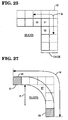
- Figure 25 illustrates the corner 53 of Figure 22, and shows the final configuration of oxide formed at the corner.
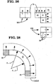
- Figure 26 illustrates how, in simplified theory, material migrates when the corner 53 in Figures 22 and 25 is oxidized.
- Figure 27 illustrates a rounded corner which is to be oxidized.
- Figure 28 illustrates, in simplified theory, how material migrates during oxidation of the rounded corner of Figure 27.
- a process according to the invention enables the sharp corner 53 shown in Figures 6 and 7A, to be rounded off to create the rounded corner 64 in Figure 7B.
- the rounding reduces the thinning shown in Figure 7A, and promotes the thicker oxide layer shown in Figure 7B.
- ROUNDING OXIDE 40 A layer of silicon dioxide, labelled ROUNDING OXIDE 40, is thermally grown upon the walls of the trench 39, as shown by the sequence of Figures 8 - 10.
- the ROUNDING OXIDE layer 40 is in the range of about 3 to 150 nanometers thick.
- the ROUNDING OXIDE 40 preferentially invades the interface 48, as does field oxide in the case of bird's beak formation. However, because the process of forming the ROUNDING OXIDE 40 is of much shorter duration than that for forming field oxide, the invasion of the interface 48 is much less. For example, if the ROUNDING OXIDE 40 is between about 10 and 80 nanometers thick (thickness is indicated by dimension D3 in Figure 10), the invasion would be expected to be about 8 to 64 nanometers (the invasion is indicated by dimension D4 in Figure 10). Following ROUNDING OXIDE 40 formation, a field implant 49 is undertaken, as indicated in Figure 10, in order to introduce dopants for creation of sources and drains.
- a sealing nitride layer 70 in Figure 11 is deposited over the ROUNDING OXIDE 40 and pad oxide 33.
- the sealing nitride is in the range of 5 to 250 nanometers in thickness. As described in the Background, the sealing nitride functions primarily to retard invasion the of oxygen into the interface 48 during field oxide growth.
- an oxide layer 73 (termed Low Temperature Oxide, LTO) is formed on the nitride layer by a low-temperature process, as shown in Figure 12.
- LTO Low Temperature Oxide
- the LTO is in the range of 10 to 250 nanometers in thickness.
- an anisotropic etch clears the bottom of the trench, as shown in Figure 13.
- field oxide is thermally grown in the trench 39, as shown in Figure 14, consuming and bending the nitride layers into approximately the configurations shown. A rounded corner 64 is present.
- the sealing nitride layer 70 is approximately conformal to the etched-back ROUNDING OXIDE 40 layer, the sealing nitride layers on the side walls 50 will likewise be parallel. With such parallel walls in Figure 17, an anisotropic etch of the bottom 77 of the trench 39 can be undertaken without a protective LTO layer. The main reason is that the protrusions such as 79 in Figure 11 are absent: the walls 50 are parallel, so that the incoming ions do not strike the walls 50, but strike only the bottom 77 of the trench 39, etching the materials at the bottom only.
- field oxide is grown as shown in Figure 18. Again, as in Figure 13, a rounded corner 64 is present.
- the structure is etched to expose the silicon and the field oxide, providing the structure shown in Figure 19.
- Gate oxide is deposited, forming the layer indicated in Figure 7B, which lacks the thinning present in Figure 7A, because of the rounded corner 64.
- the oxide growth occurs when incoming oxygen bonds with silicon and forms a solid structure of silicon dioxide.
- a given number of silicon atoms occupies a volume which is about 44 % of the volume of the same number of atoms after oxidation. That is, one million silicon atoms in a solid state occupy about 44 % of the volume of one million atoms of silicon dioxide.
- this 44 % quantity will be rounded to 50 % for simplicity: silicon is viewed as doubling in volume when it oxidizes.
- Figure 20 shows oxidation of a silicon surface.
- the previous surface 78 of silicon becomes located at the center of the oxide (under the 50% assumption). That is, oxidation occurs within the body of the silicon, and the oxidized silicon expands and extends beyond the surface 78.
- the previous surface 78 can be viewed as moving outward, perpendicular to the previous surface, as indicated by the sequence in Figure 23.
- the layer thickness L in Figure 23 is two nanometers.
- the area of the quarter circle is (pi)(8 2 )/4, or 16(pi) square nanometers.
- oxide from a region about six nanometers long ie. 16(pi)/8
- Hatched area 84 must now be about 6 nanometers long. In contrast, in Example 1, this hatched area was about 1.5 nanometers long.
- the relative thinning becomes greater as layer thickness increases.
- the invention reconfigures the silicon surface such that the quarter circle 83 in Figure 23 is broken into several sectors, two of which are shown in Figure 24, which are separated from each other. With multiple, separated sectors 83A, the thinning will be lessened, for two main reasons. First, each sector requires a smaller volume of donated material, and, second, a greater surface area of silicon is involved in making the donations. As to the second reason, in the case of Figure 23, only two regions 86 were involved in making donations to the quarter circle 83. In contrast, in Figure 24, each sector receives donations from two regions 86, making a total of four donating regions. Thus, in Figure 24, the donations are spread over four regions instead of two, and thinning is lessened.
- Figure 24 shows a single facet 87 replacing the corner 81.
- multiple facets and multiple sectors can be used, and the principles discussed above still apply.
- a curved surface can be used, and treated as having multiple facets.
- the invention reconfigures the sharp corner such that a larger proportionate volume of silicon supplies the surface area over which thinning otherwise would occur.
- the proportionality is between the volume supplying the surface and the surface area supplied.
- Figures 25 and 26 illustrate this concept of proportionate volume.
- Figure 25 shows a sharp corner.
- the silicon enclosed in the cubes having solid walls 88 supplies the oxide layer, as indicated by the respective arrows in Figure 26.
- each cube 90A supplies only a single phantom cube.
- the three cubes 90 - 92 are required to supply five adjacent phantom cubes in Figure 26.
- the oxide supplied by these three cubes is thinned.
- the remaining four cubes 90A supply only four phantom cubes; no thinning occurs here.
- the volume of cubes 90 - 92 is distributed over a surface area of length M.
- the length of M is 4 units, and so, assuming the thickness (into the paper) is one unit, the area is 4 square units.
- the total volume of cubes 90 - 92 is 3 cubic units. Thus, the ratio of surface to volume is 4/3, or 1.33.
- the same computation will be made for the rounded corner of Figure 27.
- the area represented by length M is ⁇ 1/4 x [(pi) x 8] ⁇ + 2, or about 8.3 square units.
- the volume of silicon which supplies this area of length M is that within (a) region 97 plus (b) the two hatched cubes 99.
- Region 97 has a volume of [(pi x 4 2 ) - (pi x 3 2 )]/4, or about 5.5 cubic units. Adding the two hatched cubes (one cubic unit each) to this volume gives a total volume of about 7.5 cubic units.
- a volume of about 7.5 cubic units supplies an area of about 8.3 square units.
- the ratio of surface area to volume is about 8.3/7.5, or about 1.11.
- the surface/volume ratio has decreased in Figure 27, as compared with Figure 25, indicating that the oxide layer will be thicker.
- the invention deceases the ratio of (a) surface area supplied to (b) volume of silicon precursor supplying the area. From a converse perspective, the proportionate volume supplying a given area is increased: under the syrup analogy, the amount of syrup supplying the pan is increased. Similarly, the volume of silicon per unit area of silicon surface to be oxidized is increased.
- the rounded corner 64 in Figure 7 can be viewed as a flare in the entrance to the trench.
- the flare removes the sharp corner, indicated by the phantom line 50 in Figure 1C.
- the sharp corner 53 in Figure 7A can be viewed as a protrusion.
- gate oxide is deposited over the protrusion, thinning occurs, as discussed above.
- the invention blunts the protrusion, by forming it into facets.
- the rounded (or blunted) corner 64 of Figure 7B can be viewed as an edge of a higher radius of curvature, as compared with the corner 53 in Figure 7A, which has a lower radius of curvature.
- a corner has a radius of curvature of zero, and a straight line has an infinite radius.
- the described method can be viewed as forming a small bird's beak at the edge of the interface 48 in Figure 9 between the pad oxide and the silicon, followed by sealing the edge against further bird's beak formation during field oxide growth. That is, a pre-oxidation is undertaken. After field oxide growth has been completed, the final bird's beak is smaller that which would exist if the field oxide were formed with no sealing nitride present.
- bird's beak is defined in the art. One definition refers to the oxide structure formed below an oxide layer located atop a silicon layer, and having an edge exposed to oxygen which invades along the interface in order to form the beak. The bird's beak decreases in thickness as distance from the edge increases.
- the preferred radius of curvature of the connecting surface is determined with reference to the oxide layer thickness. That is, if the oxide is extremely thin, a sharp corner may pose no problem, because the quarter circle 83 of Figure 23 is of such a small area that the contributions from neighboring oxide are insignificant. Conversely, if the oxide is thick, the contributions become significant.
- radius of curvature R in Figure 27 be at least 30 nanometers.
- radius of curvature can refer to an average radius approximated by a pair of curves 102A and 102B which sandwich the facets.
- the invention can be viewed as forming a collar of oxide, in the form of the oxide forming the small bird's beak in Figure 10, around the trench 39.
- an important aspect of the invention is the attainment of the rounded corner 64 in Figure 7B, prior to formation of the gate oxide layer 52.
- the steps which produce this rounded corner are one form of the invention.
Landscapes
- Local Oxidation Of Silicon (AREA)
- Element Separation (AREA)
Description
- This invention relates to the manufacture of semiconductor integrated circuit devices.
- In the fabrication of integrated circuits, a phenomenon known as "bird's beak" sometimes occurs. Figures 1A and 1B illustrate an example. Figure 1A shows four components: a
silicon substrate 30, apad oxide layer 33, asilicon nitride layer 36, and atrench 39 formed in the preceding three components. After trench formation, afield oxide 43 in Figure 1B is thermally grown in the trench, by introducing oxygen at an elevated temperature. - For various technical reasons, the
field oxide 43 does not penetrate to a uniform depth into thesidewalls 50 of the silicon in Figure 1A. Instead, the incoming oxygen (which forms the oxide 43) diffuses deeper in the vicinity of theinterface 48 between the pad oxide and silicon. For example, oxide depth D1 in Figure 1B is deeper than depth D2. Moreover, in general, the change in depth is not linear:profile 52 is a curved line. - The
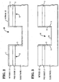
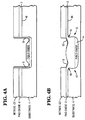
profile 52 of the oxide structure is known as a bird's beak. Bird's beaks are undesirable because they occupy space which could otherwise be used for circuit elements, such as transistors. - One solution to the formation of bird's beaks is disclosed in U.S. patent 4,923,563. Figures 2, 3, 4A, 4B, and 5 herein are copied from the patent, but with some numerals added for reference.
- In Figure 2, a
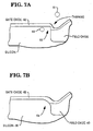
trench 39 is created similar to that of Figure 1A. Next, a nitride layer 7, havingsidewalls 9, is applied by low pressure chemical vapor deposition. Next, as shown in Figure 3, the bottom of the nitride layer 7 is removed, exposing the underlying silicon at thetrench bottom 8. Then, as shown by the sequence of Figures 4A, 4B, and 5, field oxide is grown in the trench. However, oxide invasion into theinterface 48 does not occur to a significant extent at this time, because thesidewall nitride layer 9 covers the edge of the interface and inhibits oxygen penetration. A large bird's beak is not formed as in Figure 1B. - In some situations, the approach described above in reducing bird's beaks can result in a disadvantage. One example is shown in Figures 6 and 7. The structure of Figure 6 was derived by etching away the pad oxide of Figure 5. During the etching process, some field oxide is also etched away, as in
region 57. If a bird's beak in Figure 1C is not present, thesloped profile 52 is not present, so that etching of the field oxide can result in asharp corner 53, in Figures 1C and 6, where the field oxide meets the silicon. Whengate oxide 52 in Figure 7 is formed over thecorner 53, the corner can cause the gate oxide to be formed in an undesirably thin layer, as indicated in Figure 7A. The thin gate oxide can structurally fail, and cease to act as an electrical insulator, allowingregions - US Patent 4580330 discloses a method of fabricating an integrated circuit device in which a recess is formed in a silicon substrate and a sidewall pad oxide layer is formed on the sides of the said recess and so as to extend over a corner formed in the substrate and into an undercut formed in an oxide layer overlying said substrate. The method serves merely to obtain a secure joint between a first nitride layer formed above the oxide layer and a sidewall nitride layer formed over the sidewalls of the recess.
- It is an object of the present invention to provide a process for integrated circuit manufacture in which bird's beaks may be reduced without causing a structural configuration which induces thinning of a subsequently formed layer formed at the location prone to bird's beak formation.
- Therefore, according to the present invention, there is provided a method of processing a semiconductor device having a silicon substrate, comprising the steps of forming a pad oxide layer on said substrate, forming a trench through said pad oxide layer and into said silicon substrate, blunting the comer of the silicon substrate found at the sidewall of the trench at the point of interface between the silicon substrate and said pad oxide layer by the formation of rounding oxide at said region, forming a silicon nitride protection layer to extend over said rounding oxide at said region, exposing the base of said trench and thermally growing field oxide in said trench, exposing said blunted comer and forming an oxide layer to extend over said blunted corner, the method comprising the step of, prior to said step of forming said silicon nitride protection layer, partially removing said layer of rounding oxide from the side walls of said trench to form substantially planar and parallel surfaces of the rounding oxide on the side walls of the trench.
- One embodiment of the invention will now be described by way of example, with reference to the accompanying drawings, in which:-
- Figures 1A and 1B show an intermediate structure in the fabrication of an electronic integrated circuit, and Figure 1B shows a bird's beak.
- Figure 1C shows a
sharp corner 53 can exist when a bird's beak in Figure 1B is prevented from forming. - Figures 2, 3, 4A, 4B, and 5 illustrate steps which inhibit formation of a bird's beak.
- Figure 6 illustrates that the
sharp corner 53 in Figure 1C can be exposed during a fabrication step. - Figure 7 illustrates formation of a
gate oxide layer 52 over thesharp corner 53 of Figure 6. - Figure 7A illustrates how the
sharp corner 53 can cause the gate oxide of Figure 7 to become thin. - Figure 7B illustrates one form of the invention: the corner of Figure 7A has been rounded.
- Figures 8 - 14 illustrate a sequence of steps by which bird's beak can be reduced, yet without formation of the
sharp corner 53 in Figure 1C. - Figures 15 - 18 illustrate an alternate procedure to that of Figures 8 - 14.
- Figure 19 illustrates an intermediate structure formed by the present invention, which can be derived from the structures of either Figure 14 or 18.
- Figure 20 illustrates, in simplified form, how oxide grows in silicon.
- Figure 21 illustrates schematically how
surface 78 moves perpendicularly during the growth of Figure 20. - Figure 22 illustrates schematically how the perpendicular growth of Figure 21 can, in theory, result in a
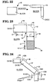
vacant corner 81 at which no oxide is present. - Figure 23 is an enlargement of the region of the
vacant corner 81 of Figure 22. - Figure 24 illustrates a reconfiguration of the
corner 53 in Figure 22. - Figure 25 illustrates the
corner 53 of Figure 22, and shows the final configuration of oxide formed at the corner. - Figure 26 illustrates how, in simplified theory, material migrates when the
corner 53 in Figures 22 and 25 is oxidized. - Figure 27 illustrates a rounded corner which is to be oxidized.
- Figure 28 illustrates, in simplified theory, how material migrates during oxidation of the rounded corner of Figure 27.
- In simplified terms, a process according to the invention enables the
sharp corner 53 shown in Figures 6 and 7A, to be rounded off to create therounded corner 64 in Figure 7B. The rounding reduces the thinning shown in Figure 7A, and promotes the thicker oxide layer shown in Figure 7B. - The preferred method can begin with the structure shown in Figure 1A. A layer of silicon dioxide, labelled
ROUNDING OXIDE 40, is thermally grown upon the walls of thetrench 39, as shown by the sequence of Figures 8 - 10. The ROUNDINGOXIDE layer 40 is in the range of about 3 to 150 nanometers thick. - The ROUNDING
OXIDE 40 preferentially invades theinterface 48, as does field oxide in the case of bird's beak formation. However, because the process of forming the ROUNDINGOXIDE 40 is of much shorter duration than that for forming field oxide, the invasion of theinterface 48 is much less. For example, if the ROUNDINGOXIDE 40 is between about 10 and 80 nanometers thick (thickness is indicated by dimension D3 in Figure 10), the invasion would be expected to be about 8 to 64 nanometers (the invasion is indicated by dimension D4 in Figure 10). Following ROUNDINGOXIDE 40 formation, afield implant 49 is undertaken, as indicated in Figure 10, in order to introduce dopants for creation of sources and drains. - After field implantation, one of two alternate procedures can be performed in preparation for formation of field oxide. In the first procedure which relates to the subject matter of the invention but does not illustrated an embodiment thereof, a
sealing nitride layer 70 in Figure 11 is deposited over theROUNDING OXIDE 40 andpad oxide 33. The sealing nitride is in the range of 5 to 250 nanometers in thickness. As described in the Background, the sealing nitride functions primarily to retard invasion the of oxygen into theinterface 48 during field oxide growth. - Next, an oxide layer 73 (termed Low Temperature Oxide, LTO) is formed on the nitride layer by a low-temperature process, as shown in Figure 12. The LTO is in the range of 10 to 250 nanometers in thickness. Then, an anisotropic etch clears the bottom of the trench, as shown in Figure 13. Finally, field oxide is thermally grown in the
trench 39, as shown in Figure 14, consuming and bending the nitride layers into approximately the configurations shown. Arounded corner 64 is present. - In the alternate procedure, prior to the application of the sealing nitride in Figure 11, the
ROUNDING OXIDE 40 layer is partially etched back, as shown in Figure 15, so that thewalls 50 form surfaces which are planar and parallel.Protrusions 79 in Figure 11 are now absent. Then, the sealingnitride layer 70 is applied, as shown in Figure 16. - Since the sealing
nitride layer 70 is approximately conformal to the etched-back ROUNDING OXIDE 40 layer, the sealing nitride layers on theside walls 50 will likewise be parallel. With such parallel walls in Figure 17, an anisotropic etch of the bottom 77 of thetrench 39 can be undertaken without a protective LTO layer. The main reason is that the protrusions such as 79 in Figure 11 are absent: thewalls 50 are parallel, so that the incoming ions do not strike thewalls 50, but strike only the bottom 77 of thetrench 39, etching the materials at the bottom only. - Following the nitride-clearing step of Figure 17, field oxide is grown as shown in Figure 18. Again, as in Figure 13, a
rounded corner 64 is present. - After growth of field oxide, the structure is etched to expose the silicon and the field oxide, providing the structure shown in Figure 19. Gate oxide is deposited, forming the layer indicated in Figure 7B, which lacks the thinning present in Figure 7A, because of the
rounded corner 64. - 1. There are several ways to explain why the invention is effective in mitigating oxide thinning at corners, including the following. The oxide growth occurs when incoming oxygen bonds with silicon and forms a solid structure of silicon dioxide. As a rough approximation, a given number of silicon atoms occupies a volume which is about 44 % of the volume of the same number of atoms after oxidation. That is, one million silicon atoms in a solid state occupy about 44 % of the volume of one million atoms of silicon dioxide. [See pages 343, 344 of S. M. Sze, Semiconductor Devices, Physics and Technology (John Wiley, New York, 1985)] For present purposes, this 44 % quantity will be rounded to 50 % for simplicity: silicon is viewed as doubling in volume when it oxidizes.
- Figure 20 shows oxidation of a silicon surface. The
previous surface 78 of silicon becomes located at the center of the oxide (under the 50% assumption). That is, oxidation occurs within the body of the silicon, and the oxidized silicon expands and extends beyond thesurface 78. For present purposes, theprevious surface 78 can be viewed as moving outward, perpendicular to the previous surface, as indicated by the sequence in Figure 23. - When a square corner oxidizes, such as the
corner 53 in Figure 7A, after a given amount of oxidation has occurred, the parallel movement shown in Figure 21 would cause the oxide configuration shown in Figure 22. (Figure 22 is a simplification made for the purposes of explaining why thinning occurs; the configuration of this Figure probably does not actually occur.) Because the oxide surface is assumed to grow perpendicular to the initial silicon surface, there is no oxide formed insquare 81; it remains empty. If an oxide layer is to be formed around the corner, thequarter circle 83 in Figure 23 must be filled with oxide. This filling oxide must be donated by neighboring oxide. The donations will cause the thinning discussed above, as the following numerical example will illustrate. - Let it be assumed that the layer thickness L in Figure 23 is two nanometers. The area of the
quarter circle 83 is thus (pi)(2)2/4, or 3.14 square nanometers. Since each linear nanometer (dimension L2) of the surface is covered by 2 square nanometers of oxide (L2 x L = 2), about 1.5 linear nanometers (ie, 3.14/2) must be depleted and contributed to the quarter circle. Hatchedarea 84 represents the depleted area. Of course, an entire hatched area is not donated to the quarter circle, but, instead, the donations will be made by several different areas, causing a distributed thinning. - Clearly, filling the
quarter circle 83 will cause a thinning in the oxide layer near thecorner 53, because neighboring oxide must be depleted and contributed to the quarter circle. Moreover, as the oxide layer becomes thicker, the relative thinning worsens, because the area of thequarter circle 83 increases as the square of layer thickness. An example will illustrate the worsening in relative thinning. - If the thickness L is 8 nanometers, instead of the two nanometers discussed above, the area of the quarter circle is (pi)(82)/4, or 16(pi) square nanometers. One linear nanometer (L2) of surface is now covered by eight square nanometers of oxide (L2 x L = 8). To obtain 16(pi) square nanometers to supply the
quarter circle 83, oxide from a region about six nanometers long (ie. 16(pi)/8) must be depleted and contributed into the quarter circle. Hatchedarea 84 must now be about 6 nanometers long. In contrast, in Example 1, this hatched area was about 1.5 nanometers long. Thus, the relative thinning becomes greater as layer thickness increases. - Therefore, it has been shown in a general fashion why thinning of oxide occurs at a corner. One explanation will now be given of why the invention reduces oxide thinning.
- From one point of view, the invention reconfigures the silicon surface such that the
quarter circle 83 in Figure 23 is broken into several sectors, two of which are shown in Figure 24, which are separated from each other. With multiple, separatedsectors 83A, the thinning will be lessened, for two main reasons. First, each sector requires a smaller volume of donated material, and, second, a greater surface area of silicon is involved in making the donations. As to the second reason, in the case of Figure 23, only tworegions 86 were involved in making donations to thequarter circle 83. In contrast, in Figure 24, each sector receives donations from tworegions 86, making a total of four donating regions. Thus, in Figure 24, the donations are spread over four regions instead of two, and thinning is lessened. - Figure 24 shows a
single facet 87 replacing thecorner 81. However, multiple facets and multiple sectors can be used, and the principles discussed above still apply. Further, a curved surface can be used, and treated as having multiple facets. - From another point of view, the invention reconfigures the sharp corner such that a larger proportionate volume of silicon supplies the surface area over which thinning otherwise would occur. The proportionality is between the volume supplying the surface and the surface area supplied. Figures 25 and 26 illustrate this concept of proportionate volume.
- Figure 25 shows a sharp corner. During oxidation, the silicon enclosed in the cubes having
solid walls 88 supplies the oxide layer, as indicated by the respective arrows in Figure 26. Forcubes 90A, material migration is only in a direction perpendicular to their surface; eachcube 90A supplies only a single phantom cube. However, the three cubes 90 - 92 are required to supply five adjacent phantom cubes in Figure 26. For these cubes, there is lateral (ie, along the surface 78) as well as perpendicular migration. The oxide supplied by these three cubes is thinned. In contrast, the remaining fourcubes 90A supply only four phantom cubes; no thinning occurs here. - If the corner is replaced by a curved corner, as shown in Figure 27, a greater proportionate volume (ie,
swath 97 plus cubes 99) now supplies the oxide, and thinning is reduced. The concept of a greater proportionate volume will now be explained. - In Figure 25, the volume of cubes 90 - 92 is distributed over a surface area of length M. The length of M is 4 units, and so, assuming the thickness (into the paper) is one unit, the area is 4 square units. The total volume of cubes 90 - 92 is 3 cubic units. Thus, the ratio of surface to volume is 4/3, or 1.33.
- The same computation will be made for the rounded corner of Figure 27. The area represented by length M is {1/4 x [(pi) x 8]} + 2, or about 8.3 square units.
- The volume of silicon which supplies this area of length M is that within (a)
region 97 plus (b) the two hatchedcubes 99.Region 97 has a volume of [(pi x 42) - (pi x 32)]/4, or about 5.5 cubic units. Adding the two hatched cubes (one cubic unit each) to this volume gives a total volume of about 7.5 cubic units. - Therefore, for Figure 27, a volume of about 7.5 cubic units supplies an area of about 8.3 square units. The ratio of surface area to volume is about 8.3/7.5, or about 1.11. The surface/volume ratio has decreased in Figure 27, as compared with Figure 25, indicating that the oxide layer will be thicker.
- Therefore, from this perspective, the invention deceases the ratio of (a) surface area supplied to (b) volume of silicon precursor supplying the area. From a converse perspective, the proportionate volume supplying a given area is increased: under the syrup analogy, the amount of syrup supplying the pan is increased. Similarly, the volume of silicon per unit area of silicon surface to be oxidized is increased.
- It is recognized that the computations given above do not predict the exact thickness of oxide which will be obtained. One reason is that the migration pattern is not known and, even if known, will change with such parameters as temperature, reaction time, etc. One result of this lack of knowledge is that the
length 86 in Figure 23 of the regions supplying thequarter circle 83 is not known. Nevertheless, the computations are given in order to illustrate the broad principle that oxide thinning occurs at sharp corners. - 2. The
rounded corner 64 in Figure 7 can be viewed as a flare in the entrance to the trench. The flare removes the sharp corner, indicated by thephantom line 50 in Figure 1C. - 3. The
sharp corner 53 in Figure 7A can be viewed as a protrusion. When gate oxide is deposited over the protrusion, thinning occurs, as discussed above. The invention blunts the protrusion, by forming it into facets. - 4. The rounded (or blunted)
corner 64 of Figure 7B can be viewed as an edge of a higher radius of curvature, as compared with thecorner 53 in Figure 7A, which has a lower radius of curvature. In theory, a corner has a radius of curvature of zero, and a straight line has an infinite radius. - 5. The described method can be viewed as forming a small bird's beak at the edge of the
interface 48 in Figure 9 between the pad oxide and the silicon, followed by sealing the edge against further bird's beak formation during field oxide growth. That is, a pre-oxidation is undertaken. After field oxide growth has been completed, the final bird's beak is smaller that which would exist if the field oxide were formed with no sealing nitride present. - The term "bird's beak" is defined in the art. One definition refers to the oxide structure formed below an oxide layer located atop a silicon layer, and having an edge exposed to oxygen which invades along the interface in order to form the beak. The bird's beak decreases in thickness as distance from the edge increases.
- In one form of the invention, the preferred radius of curvature of the connecting surface is determined with reference to the oxide layer thickness. That is, if the oxide is extremely thin, a sharp corner may pose no problem, because the
quarter circle 83 of Figure 23 is of such a small area that the contributions from neighboring oxide are insignificant. Conversely, if the oxide is thick, the contributions become significant. - It is preferred that the radius of curvature R in Figure 27 be at least 30 nanometers. For faceted surfaces, which are not curved, such as those shown in Figure 24, the term "radius of curvature" can refer to an average radius approximated by a pair of
curves - 6. The invention can be viewed as forming a collar of oxide, in the form of the oxide forming the small bird's beak in Figure 10, around the
trench 39. - 7. Detailed technical specifications for carrying out the steps described above have not been given, because methods of executing these steps are well known in the art.
- 8. From one point of view, an important aspect of the invention is the attainment of the
rounded corner 64 in Figure 7B, prior to formation of thegate oxide layer 52. The steps which produce this rounded corner are one form of the invention.
Claims (1)
- A method of processing a semiconductor device having a silicon substrate (30), comprising the steps of forming a pad oxide layer (33) on said substrate (30), forming a trench (39) through said pad oxide layer (33) and into said silicon substrate (30), blunting the corner (53) of the silicon substrate (30) found at the sidewall of the trench (39) at the point of interface between the silicon substrate (30) and said pad oxide layer (33) by the formation of rounding oxide (40) at said region, forming a silicon nitride protection layer (70) to extend over said rounding oxide at said region, exposing the base of said trench (39) and thermally growing field oxide (43) in said trench (39), exposing said blunted corner (53) and forming an oxide layer (52) to extend over said blunted comer (53), the method comprising the step of, prior to said step of forming said silicon nitride protection layer (70), partially removing said layer of rounding oxide (40) from the side walls of said trench (39) to form substantially planar and parallel surfaces of the rounding oxide on the side walls of the trench.
Applications Claiming Priority (2)
| Application Number | Priority Date | Filing Date | Title |
|---|---|---|---|
| US66334991A | 1991-03-04 | 1991-03-04 | |
| US663349 | 1991-03-04 |
Publications (3)
| Publication Number | Publication Date |
|---|---|
| EP0502663A2 EP0502663A2 (en) | 1992-09-09 |
| EP0502663A3 EP0502663A3 (en) | 1993-09-08 |
| EP0502663B1 true EP0502663B1 (en) | 2001-09-05 |
Family
ID=24661438
Family Applications (1)
| Application Number | Title | Priority Date | Filing Date |
|---|---|---|---|
| EP92301710A Expired - Lifetime EP0502663B1 (en) | 1991-03-04 | 1992-02-28 | Semiconductor device processing method providing isolation regions in a semi-conductor substrate |
Country Status (3)
| Country | Link |
|---|---|
| EP (1) | EP0502663B1 (en) |
| JP (1) | JPH05102133A (en) |
| DE (1) | DE69232038T2 (en) |
Families Citing this family (1)
| Publication number | Priority date | Publication date | Assignee | Title |
|---|---|---|---|---|
| US5470783A (en) * | 1994-06-06 | 1995-11-28 | At&T Ipm Corp. | Method for integrated circuit device isolation |
Family Cites Families (3)
| Publication number | Priority date | Publication date | Assignee | Title |
|---|---|---|---|---|
| EP0052948A1 (en) * | 1980-11-24 | 1982-06-02 | Motorola, Inc. | Oxide isolation process |
| US4580330A (en) * | 1984-06-15 | 1986-04-08 | Texas Instruments Incorporated | Integrated circuit isolation |
| US4923563A (en) * | 1987-06-15 | 1990-05-08 | Ncr Corporation | Semiconductor field oxide formation process using a sealing sidewall of consumable nitride |
-
1992
- 1992-02-28 DE DE69232038T patent/DE69232038T2/en not_active Expired - Lifetime
- 1992-02-28 JP JP4075745A patent/JPH05102133A/en active Pending
- 1992-02-28 EP EP92301710A patent/EP0502663B1/en not_active Expired - Lifetime
Also Published As
| Publication number | Publication date |
|---|---|
| EP0502663A2 (en) | 1992-09-09 |
| DE69232038T2 (en) | 2002-01-31 |
| EP0502663A3 (en) | 1993-09-08 |
| JPH05102133A (en) | 1993-04-23 |
| DE69232038D1 (en) | 2001-10-11 |
Similar Documents
| Publication | Publication Date | Title |
|---|---|---|
| US5445989A (en) | Method of forming device isolation regions | |
| US5945724A (en) | Trench isolation region for semiconductor device | |
| US4965221A (en) | Spacer isolation method for minimizing parasitic sidewall capacitance and creating fully recessed field oxide regions | |
| KR0176153B1 (en) | A device isolation film and method for forming the same in a semiconductor device | |
| US6372601B1 (en) | Isolation region forming methods | |
| CN87104640A (en) | Integrated circuit insulation process | |
| JPH06232061A (en) | Forming single crystal region by selective epitaxy | |
| JPS6175539A (en) | Manufacture of integrated circuit | |
| JPH05144806A (en) | Semiconductor device having recessed and sidewall-sealed poly-buffer-type locos separator and method of manufacturing the same | |
| JP2900503B2 (en) | Method of manufacturing a trench insulation structure in a semiconductor substrate | |
| US5453395A (en) | Isolation technology using liquid phase deposition | |
| JPH02119261A (en) | Trench side face wall doping method by utilizing oxide film and nitride film and semiconductor element | |
| US6551925B2 (en) | Method of forming a trench isolation structure resistant to hot phosphoric acid by extending trench liner to shoulder portions | |
| EP0592024B1 (en) | Etching silicon nitride in a process comprising selective oxidation of a trench side wall in a semiconductor wafer | |
| US5554562A (en) | Advanced isolation scheme for deep submicron technology | |
| KR100353174B1 (en) | Method for fabrication of silicon on insulator substrates | |
| JPS63299144A (en) | Method of separating interface sealed by oxide protective layer for pad | |
| EP0502663A2 (en) | Semiconductor device processing method providing isolation regions in a semi-conductor substrate | |
| US6150072A (en) | Method of manufacturing a shallow trench isolation structure for a semiconductor device | |
| US6586314B1 (en) | Method of forming shallow trench isolation regions with improved corner rounding | |
| EP0293979A2 (en) | Zero bird-beak oxide isolation scheme for integrated circuits | |
| USRE34400E (en) | Method for fabricating isolation region in semiconductor devices | |
| US6261966B1 (en) | Method for improving trench isolation | |
| US20040180550A1 (en) | Method for forming shallow trench isolation with control of bird beak | |
| KR960005044B1 (en) | Semiconductor Device Separation Method |
Legal Events
| Date | Code | Title | Description |
|---|---|---|---|
| PUAI | Public reference made under article 153(3) epc to a published international application that has entered the european phase |
Free format text: ORIGINAL CODE: 0009012 |
|
| AK | Designated contracting states |
Kind code of ref document: A2 Designated state(s): DE GB NL |
|
| PUAL | Search report despatched |
Free format text: ORIGINAL CODE: 0009013 |
|
| AK | Designated contracting states |
Kind code of ref document: A3 Designated state(s): DE GB NL |
|
| 17P | Request for examination filed |
Effective date: 19940214 |
|
| RAP1 | Party data changed (applicant data changed or rights of an application transferred) |
Owner name: AT&T GLOBAL INFORMATION SOLUTIONS INTERNATIONAL IN |
|
| 17Q | First examination report despatched |
Effective date: 19950308 |
|
| RAP1 | Party data changed (applicant data changed or rights of an application transferred) |
Owner name: HYUNDAI ELECTRONICS AMERICA Owner name: AT&T GLOBAL INFORMATION SOLUTIONS INTERNATIONAL IN |
|
| RAP1 | Party data changed (applicant data changed or rights of an application transferred) |
Owner name: SYMBIOS LOGIC INC. Owner name: HYUNDAI ELECTRONICS AMERICA Owner name: AT&T GLOBAL INFORMATION SOLUTIONS INTERNATIONAL IN |
|
| APAB | Appeal dossier modified |
Free format text: ORIGINAL CODE: EPIDOS NOAPE |
|
| APAD | Appeal reference recorded |
Free format text: ORIGINAL CODE: EPIDOS REFNE |
|
| RAP1 | Party data changed (applicant data changed or rights of an application transferred) |
Owner name: SYMBIOS LOGIC INC. Owner name: NCR INTERNATIONAL, INC. Owner name: HYUNDAI ELECTRONICS AMERICA |
|
| RAP1 | Party data changed (applicant data changed or rights of an application transferred) |
Owner name: SYMBIOS, INC. Owner name: NCR INTERNATIONAL, INC. Owner name: HYUNDAI ELECTRONICS AMERICA |
|
| APAD | Appeal reference recorded |
Free format text: ORIGINAL CODE: EPIDOS REFNE |
|
| APAB | Appeal dossier modified |
Free format text: ORIGINAL CODE: EPIDOS NOAPE |
|
| APBJ | Interlocutory revision of appeal recorded |
Free format text: ORIGINAL CODE: EPIDOS IRAPE |
|
| GRAG | Despatch of communication of intention to grant |
Free format text: ORIGINAL CODE: EPIDOS AGRA |
|
| GRAH | Despatch of communication of intention to grant a patent |
Free format text: ORIGINAL CODE: EPIDOS IGRA |
|
| GRAH | Despatch of communication of intention to grant a patent |
Free format text: ORIGINAL CODE: EPIDOS IGRA |
|
| GRAH | Despatch of communication of intention to grant a patent |
Free format text: ORIGINAL CODE: EPIDOS IGRA |
|
| GRAA | (expected) grant |
Free format text: ORIGINAL CODE: 0009210 |
|
| AK | Designated contracting states |
Kind code of ref document: B1 Designated state(s): DE GB NL |
|
| REF | Corresponds to: |
Ref document number: 69232038 Country of ref document: DE Date of ref document: 20011011 |
|
| REG | Reference to a national code |
Ref country code: GB Ref legal event code: IF02 |
|
| PLBE | No opposition filed within time limit |
Free format text: ORIGINAL CODE: 0009261 |
|
| 26N | No opposition filed | ||
| NLS | Nl: assignments of ep-patents |
Owner name: NCR INTERNATIONAL, INC Owner name: HYNIX SEMICONDUCTOR INC. Owner name: HYUNDAI ELECTRONICS AMERICA |
|
| NLT1 | Nl: modifications of names registered in virtue of documents presented to the patent office pursuant to art. 16 a, paragraph 1 |
Owner name: NCR INTERNATIONAL, INC Owner name: HYNIX SEMICONDUCTOR AMERICA INC. |
|
| REG | Reference to a national code |
Ref country code: GB Ref legal event code: 732E |
|
| APAH | Appeal reference modified |
Free format text: ORIGINAL CODE: EPIDOSCREFNO |
|
| REG | Reference to a national code |
Ref country code: GB Ref legal event code: 732E |
|
| REG | Reference to a national code |
Ref country code: GB Ref legal event code: 732E |
|
| NLS | Nl: assignments of ep-patents |
Owner name: MAGNACHIP SEMICONDUCTOR LTD. Effective date: 20090428 Owner name: NCR INTERNATIONAL, INC Effective date: 20090428 |
|
| PGFP | Annual fee paid to national office [announced via postgrant information from national office to epo] |
Ref country code: NL Payment date: 20110228 Year of fee payment: 20 Ref country code: DE Payment date: 20110225 Year of fee payment: 20 |
|
| PGFP | Annual fee paid to national office [announced via postgrant information from national office to epo] |
Ref country code: GB Payment date: 20110223 Year of fee payment: 20 |
|
| REG | Reference to a national code |
Ref country code: DE Ref legal event code: R071 Ref document number: 69232038 Country of ref document: DE |
|
| REG | Reference to a national code |
Ref country code: DE Ref legal event code: R071 Ref document number: 69232038 Country of ref document: DE |
|
| REG | Reference to a national code |
Ref country code: NL Ref legal event code: V4 Effective date: 20120228 |
|
| REG | Reference to a national code |
Ref country code: GB Ref legal event code: PE20 Expiry date: 20120227 |
|
| PG25 | Lapsed in a contracting state [announced via postgrant information from national office to epo] |
Ref country code: DE Free format text: LAPSE BECAUSE OF EXPIRATION OF PROTECTION Effective date: 20120229 |
|
| PG25 | Lapsed in a contracting state [announced via postgrant information from national office to epo] |
Ref country code: GB Free format text: LAPSE BECAUSE OF EXPIRATION OF PROTECTION Effective date: 20120227 |