EP0501434B1 - Use of a garnet thin film in a magnetostatic-wave device - Google Patents
Use of a garnet thin film in a magnetostatic-wave device Download PDFInfo
- Publication number
- EP0501434B1 EP0501434B1 EP19920103222 EP92103222A EP0501434B1 EP 0501434 B1 EP0501434 B1 EP 0501434B1 EP 19920103222 EP19920103222 EP 19920103222 EP 92103222 A EP92103222 A EP 92103222A EP 0501434 B1 EP0501434 B1 EP 0501434B1
- Authority
- EP
- European Patent Office
- Prior art keywords
- magnetostatic
- garnet
- thin film
- composition
- falling
- Prior art date
- Legal status (The legal status is an assumption and is not a legal conclusion. Google has not performed a legal analysis and makes no representation as to the accuracy of the status listed.)
- Expired - Lifetime
Links
- 239000002223 garnet Substances 0.000 title claims description 14
- 239000010409 thin film Substances 0.000 title claims description 9
- 239000000203 mixture Substances 0.000 claims description 13
- 239000000463 material Substances 0.000 claims description 10
- 239000000758 substrate Substances 0.000 claims description 8
- 239000002902 ferrimagnetic material Substances 0.000 claims description 4
- 229910052733 gallium Inorganic materials 0.000 claims description 4
- 238000010587 phase diagram Methods 0.000 claims description 3
- 229910002056 binary alloy Inorganic materials 0.000 claims description 2
- 239000010408 film Substances 0.000 description 14
- 230000005291 magnetic effect Effects 0.000 description 8
- ZPDRQAVGXHVGTB-UHFFFAOYSA-N gallium;gadolinium(3+);oxygen(2-) Chemical compound [O-2].[O-2].[O-2].[Ga+3].[Gd+3] ZPDRQAVGXHVGTB-UHFFFAOYSA-N 0.000 description 7
- 230000005415 magnetization Effects 0.000 description 6
- 238000004943 liquid phase epitaxy Methods 0.000 description 3
- 239000000126 substance Substances 0.000 description 3
- WMWLMWRWZQELOS-UHFFFAOYSA-N bismuth(iii) oxide Chemical compound O=[Bi]O[Bi]=O WMWLMWRWZQELOS-UHFFFAOYSA-N 0.000 description 2
- 230000005293 ferrimagnetic effect Effects 0.000 description 2
- GYHNNYVSQQEPJS-UHFFFAOYSA-N Gallium Chemical compound [Ga] GYHNNYVSQQEPJS-UHFFFAOYSA-N 0.000 description 1
- 238000005336 cracking Methods 0.000 description 1
- QZQVBEXLDFYHSR-UHFFFAOYSA-N gallium(III) oxide Inorganic materials O=[Ga]O[Ga]=O QZQVBEXLDFYHSR-UHFFFAOYSA-N 0.000 description 1
- JEIPFZHSYJVQDO-UHFFFAOYSA-N iron(III) oxide Inorganic materials O=[Fe]O[Fe]=O JEIPFZHSYJVQDO-UHFFFAOYSA-N 0.000 description 1
- 238000005259 measurement Methods 0.000 description 1
- 238000000034 method Methods 0.000 description 1
- 239000012254 powdered material Substances 0.000 description 1
- 229910052761 rare earth metal Inorganic materials 0.000 description 1
- 150000002910 rare earth metals Chemical class 0.000 description 1
- 239000011369 resultant mixture Substances 0.000 description 1
- RUDFQVOCFDJEEF-UHFFFAOYSA-N yttrium(III) oxide Inorganic materials [O-2].[O-2].[O-2].[Y+3].[Y+3] RUDFQVOCFDJEEF-UHFFFAOYSA-N 0.000 description 1
Images

Classifications
-
- H—ELECTRICITY
- H03—ELECTRONIC CIRCUITRY
- H03H—IMPEDANCE NETWORKS, e.g. RESONANT CIRCUITS; RESONATORS
- H03H2/00—Networks using elements or techniques not provided for in groups H03H3/00 - H03H21/00
- H03H2/001—Networks using elements or techniques not provided for in groups H03H3/00 - H03H21/00 comprising magnetostatic wave network elements
-
- H—ELECTRICITY
- H01—ELECTRIC ELEMENTS
- H01F—MAGNETS; INDUCTANCES; TRANSFORMERS; SELECTION OF MATERIALS FOR THEIR MAGNETIC PROPERTIES
- H01F10/00—Thin magnetic films, e.g. of one-domain structure
- H01F10/08—Thin magnetic films, e.g. of one-domain structure characterised by magnetic layers
- H01F10/10—Thin magnetic films, e.g. of one-domain structure characterised by magnetic layers characterised by the composition
- H01F10/18—Thin magnetic films, e.g. of one-domain structure characterised by magnetic layers characterised by the composition being compounds
- H01F10/20—Ferrites
- H01F10/24—Garnets
- H01F10/245—Modifications for enhancing interaction with electromagnetic wave energy
Definitions
- the present invention relates to a garnet thin film used in magnetostatic-wave devices and, more particularly, a ferrimagnetic material for magnetostatic wave devices comprising a garnet thin film of the ferrimagnetic material epitaxially grown on a substrate of gadolinium-gallium-garnet.
- magnetostatic wave devices have been developed rapidly and its achievements have been reported in various papers.
- J.D. Adam, M.R. Daniel and D.K. Schroder in "Magnetostatic-wave devices move microwave design into gigaherts realm", Electronics, May, 1980, pp. 123-128.
- a new configuration for a magnetostatic wave filter is discussed by T. Nishikawa, K. Wakino, H. Taraha, T.Okada, S. Shinmura and Y. Ishikawa in "a low loss magnetostatic wave filter using parallel strip transducers", Microwave and RF Engineering, September/October 1989, pp.63-68.
- Such magnetostatic wave devices generally comprise a thin film of a ferrimagnetic material, generally, yttrium-iron-garnet (YIG) of the chemical formula Y 3 Fe 2 (FeO 4 ) 3 , grown by liquid-phase epitaxy techniques on a substrate of gadolinium-gallium-garnet (GGG) of the chemical formula Gd 3 Ga 2 (GaO 4 ) 3 .
- YIG yttrium-iron-garnet
- GGG gadolinium-gallium-garnet
- Gd 3 Ga 2 (GaO 4 ) 3 The epitaxially grown YIG film makes it possible to reduce the difference between input and output signals of the magnetostatic wave devices because of its very small magnetic resonance half linewidth ( ⁇ H).
- the YIG films have such a disadvantage that the change in saturation magnetization (4 ⁇ M s ) with temperature is large and of the order of about 2100 ppm/°C.
- it is required to choose a permanent magnet with a suitable temperature coefficient.
- it is difficult to minimize the temperature coefficient of the magnetostatic wave device because of limited kinds of permanent magnet materials and because of the fixed temperature coefficient of saturation magnetization of the YIG films.
- US-A-4,968,954 discloses materials for magnetostatic wave devices that comprise an epitaxial layer formed on a substrate of rare earth gallium garnet, having a chemical composition of the formula: Y 3-x Bi x Fe 5-y Ga y O 12 in which the subscript x takes a value in the range from 0.01 to 0.9, and the subscript y takes a value in the range from 0.49 to 1.0.
- a material for magnetostatic wave devices comprising a thin film of the material epitaxially grown on a substrate of gadolinium-gallium-garnet (GGG), said material having a composition expressed by the general formula (I): Y 3-x Bi x Fe 5-y Ga y O 12 (I) where x and y are mole fractions of Bi and Ga, 0 ⁇ x ⁇ 0.41, and 0 ⁇ y less than 0,49, said composition having a set of x and y falling in the area encompassed by a polygon ABCDE defined by points A (0, 0), B (0.23, 0), C (0.41, 1), D (0.15, 1) and E (0, 0.1) in a phase diagram of a binary system with x as abscissa and y as ordinate, except for a set of x and y falling on the point A.
- GGG gadolinium-gallium-garnet
- the present invention makes it possible to produce a ferrimagnetic thin films with any desired temperature coefficient of saturation magnetization ranging from about 500 to about 2000 ppm/°C, without causing increase in the magnetic resonance half linewidth ( ⁇ H). Accordingly, it is possible to improve the temperature characteristics of magnetostatic wave devices by the suitable choice of the permanent magnet material.
- the present invention makes it possible to produce excellent magnetic garnet films as the difference of the lattice constant between the garnet film and the GGG substrate can be minimized to not more than 0.01 ⁇ .
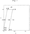
- compositions of the resultant garnet films are plotted in a binary phase diagram of Fig. 1 with x in the general formula (I) as abscissa and y in that formula as ordinate, along with the area of the composition falling in the scope of the present invention.
- the numbers in Fig. 1 correspond to the respective specimen numbers. Table 1 No.
- the magnetic resonance half linewidth ( ⁇ H) becomes more than 5 Oe, thus making it impossible to use it as a material for film in the magnetostatic wave devices.
- this composition i.e., YIG, possesses a large temperature coefficient of the saturation magnetization (4 ⁇ M s ).
- composition of the general formula (I) has been limited to those having a set of values of x and y falling in the area encompassed by the polygon ABCDE defined by the points A (0, 0), B (0.23), C (0.41, 1), D (0.15, 1) and E (0, 0.1) in Fig. 1, except for a set of x and y falling on the point A.
Landscapes
- Engineering & Computer Science (AREA)
- Physics & Mathematics (AREA)
- Electromagnetism (AREA)
- Chemical & Material Sciences (AREA)
- Materials Engineering (AREA)
- Power Engineering (AREA)
- Thin Magnetic Films (AREA)
Description
- The present invention relates to a garnet thin film used in magnetostatic-wave devices and, more particularly, a ferrimagnetic material for magnetostatic wave devices comprising a garnet thin film of the ferrimagnetic material epitaxially grown on a substrate of gadolinium-gallium-garnet.
- Recently, study of magnetostatic wave devices has developed rapidly and its achievements have been reported in various papers. For example, some examples of magnetostatic wave devices are described by J.D. Adam, M.R. Daniel and D.K. Schroder in "Magnetostatic-wave devices move microwave design into gigaherts realm", Electronics, May, 1980, pp. 123-128. Also, a new configuration for a magnetostatic wave filter is discussed by T. Nishikawa, K. Wakino, H. Taraha, T.Okada, S. Shinmura and Y. Ishikawa in "a low loss magnetostatic wave filter using parallel strip transducers", Microwave and RF Engineering, September/October 1989, pp.63-68.
- Such magnetostatic wave devices generally comprise a thin film of a ferrimagnetic material, generally, yttrium-iron-garnet (YIG) of the chemical formula Y3Fe2(FeO4)3, grown by liquid-phase epitaxy techniques on a substrate of gadolinium-gallium-garnet (GGG) of the chemical formula Gd3Ga2(GaO4)3. The epitaxially grown YIG film makes it possible to reduce the difference between input and output signals of the magnetostatic wave devices because of its very small magnetic resonance half linewidth (ΔH).
- However, the YIG films have such a disadvantage that the change in saturation magnetization (4πMs) with temperature is large and of the order of about 2100 ppm/°C. Thus, in order to improve temperature characteristics of magnetostatic-wave devices, it is required to choose a permanent magnet with a suitable temperature coefficient. However, it is difficult to minimize the temperature coefficient of the magnetostatic wave device because of limited kinds of permanent magnet materials and because of the fixed temperature coefficient of saturation magnetization of the YIG films.
- US-A-4,968,954 (Ryuo et al.) discloses materials for magnetostatic wave devices that comprise an epitaxial layer formed on a substrate of rare earth gallium garnet, having a chemical composition of the formula:
Y3-xBixFe5-yGayO12
in which the subscript x takes a value in the range from 0.01 to 0.9, and the subscript y takes a value in the range from 0.49 to 1.0. - It is therefore an object of the present invention to provide a material for magnetostatic-wave devices, which makes it possible to provide a ferrimagnetic thin film with any desired temperature coefficient of saturation magnetization (4πMs), without causing increase in magnetic resonance half linewidth (ΔH).
- According to the present invention there is provided a material for magnetostatic wave devices comprising a thin film of the material epitaxially grown on a substrate of gadolinium-gallium-garnet (GGG), said material having a composition expressed by the general formula (I):
Y3-xBixFe5-yGayO12 (I)
where x and y are mole fractions of Bi and Ga, 0 ≤ x ≤ 0.41, and 0 ≤ y less than 0,49, said composition having a set of x and y falling in the area encompassed by a polygon ABCDE defined by points A (0, 0), B (0.23, 0), C (0.41, 1), D (0.15, 1) and E (0, 0.1) in a phase diagram of a binary system with x as abscissa and y as ordinate, except for a set of x and y falling on the point A. - The present invention makes it possible to produce a ferrimagnetic thin films with any desired temperature coefficient of saturation magnetization ranging from about 500 to about 2000 ppm/°C, without causing increase in the magnetic resonance half linewidth (ΔH). Accordingly, it is possible to improve the temperature characteristics of magnetostatic wave devices by the suitable choice of the permanent magnet material.
- Further, the present invention makes it possible to produce excellent magnetic garnet films as the difference of the lattice constant between the garnet film and the GGG substrate can be minimized to not more than 0.01 Å.
- The above and other objects, features and advantages of the present invention will be understood clearly from the following explanations with reference to several examples.
- Powdered materials of Fe2O3, Y2O3, Bi2O3 and Ga2O3 were weighed and mixed so that the product has a composition of the general formula (II):
Y3-xBixFe5-yGayO12
where x and y are mole fractions of Bi and Ga and take values as shown in Table 1. Using the resultant mixtures, there were prepared magnetic garnet films on substrates of Gd3Ga5O12 by the liquid-phase epitaxy (LPE) in the same manner as Example 1. - For each garnet film produced, measurements were made on the lattice constant, saturation magnetization (4πMs), temperature coefficient (TC) of 4πMs, and magnetic resonance half linewidth (ΔH). Results are shown in Table 2. In the table, the specimens with an asterisk (*) are those out of the scope of the present invention.
- The compositions of the resultant garnet films are plotted in a binary phase diagram of Fig. 1 with x in the general formula (I) as abscissa and y in that formula as ordinate, along with the area of the composition falling in the scope of the present invention. The numbers in Fig. 1 correspond to the respective specimen numbers.
Table 1 No. x y 4πMs (G) ΔH (Oe) TC of 4πMs (ppm/°C) lattice constant (A) 1* 0 0 1800 0.6 -2100 12.376 2 0.23 0 1740 1.3 -1300 12.393 3 0 0.1 1500 0.9 -2200 12.373 4* 0 0.5 Good films were never obtained 5 0.2 0.5 950 1.4 -1700 12.381 6* 0.4 0.5 Good films were never obtained 7 0.16 1 680 2.0 -2000 12.373 8 0.41 1 630 2.5 -1500 12.393 9* 0.3 1.1 570 5.5 -1400 12.385 - As can be seen from the data for specimen No. 4 or 6, if the composition has a set of x and y falling in the area out of the line BC or the line DE, the difference in the lattice constant between the GGG substrate and the magnetic garnet film becomes more than 0.01A, causing cracking of the film, thus making it impossible to obtain garnet films with good quality.
- Further, as can be seen from the data for specimen No. 9, if the composition has a set of x and y falling in the area out of the line CD, the magnetic resonance half linewidth (ΔH) becomes more than 5 Oe, thus making it impossible to use it as a material for film in the magnetostatic wave devices.
- As can be seen from the data for specimen No. 1, this composition, i.e., YIG, possesses a large temperature coefficient of the saturation magnetization (4πMs). The composition with x = 0 and y = 0 is of course excluded from the scope of the present invention.
- For the reasons mentioned above, the composition of the general formula (I) has been limited to those having a set of values of x and y falling in the area encompassed by the polygon ABCDE defined by the points A (0, 0), B (0.23), C (0.41, 1), D (0.15, 1) and E (0, 0.1) in Fig. 1, except for a set of x and y falling on the point A.
Claims (1)
- A material of garnet thin films used in magnetostatic wave devices comprising a garnet thin film of a ferrimagnetic material epitaxially grown on a substrate of Gd3Ga2(GaO4)3, said material having a composition expressed by the general formula (I):
Y3-xBixFe5-yGayO12 (I)
where x and y are mole fractions of Bi and Ga, 0 ≤ x ≤ 0.41, and 0 ≤ y less than 0,49, said composition having a set of x and y falling in the area encompassed by a polygon ABCDE defined by points A (0, 0), B (0.23, 0), C (0.41, 1), D (0.15, 1) and E (0, 0.1) in a phase diagram of a binary system with x as abscissa and y as ordinate, except for a set of x and y falling on the point A.
Applications Claiming Priority (6)
| Application Number | Priority Date | Filing Date | Title |
|---|---|---|---|
| JP5970691A JPH04274302A (en) | 1991-02-28 | 1991-02-28 | Material for static magnetic wave device |
| JP59705/91 | 1991-02-28 | ||
| JP5970791A JPH04274303A (en) | 1991-02-28 | 1991-02-28 | Material for static magnetic wave device |
| JP59706/91 | 1991-02-28 | ||
| JP59707/91 | 1991-02-28 | ||
| JP5970591A JPH04274301A (en) | 1991-02-28 | 1991-02-28 | Material for static magnetic wave device |
Publications (3)
| Publication Number | Publication Date |
|---|---|
| EP0501434A2 EP0501434A2 (en) | 1992-09-02 |
| EP0501434A3 EP0501434A3 (en) | 1992-11-25 |
| EP0501434B1 true EP0501434B1 (en) | 1997-01-22 |
Family
ID=27296975
Family Applications (1)
| Application Number | Title | Priority Date | Filing Date |
|---|---|---|---|
| EP19920103222 Expired - Lifetime EP0501434B1 (en) | 1991-02-28 | 1992-02-26 | Use of a garnet thin film in a magnetostatic-wave device |
Country Status (2)
| Country | Link |
|---|---|
| EP (1) | EP0501434B1 (en) |
| DE (1) | DE69216871T2 (en) |
Cited By (1)
| Publication number | Priority date | Publication date | Assignee | Title |
|---|---|---|---|---|
| CN105399339A (en) * | 2015-12-18 | 2016-03-16 | 北京汽车股份有限公司 | Bismuth ferrite-based thin film containing doping elements, and preparation method thereof |
Families Citing this family (2)
| Publication number | Priority date | Publication date | Assignee | Title |
|---|---|---|---|---|
| EP0531914A3 (en) * | 1991-09-10 | 1993-07-21 | Murata Manufacturing Co., Ltd. | Magnetic thin film for magnetostatic-wave devices |
| JPH05251788A (en) * | 1992-03-04 | 1993-09-28 | Murata Mfg Co Ltd | Material for magnetostatic wave device |
Family Cites Families (1)
| Publication number | Priority date | Publication date | Assignee | Title |
|---|---|---|---|---|
| US4968954A (en) * | 1988-09-30 | 1990-11-06 | Shin-Etsu Chemical Co., Ltd. | Epitaxial layer-bearing wafer of rare earth gallium garnet for MSW device |
-
1992
- 1992-02-26 EP EP19920103222 patent/EP0501434B1/en not_active Expired - Lifetime
- 1992-02-26 DE DE1992616871 patent/DE69216871T2/en not_active Expired - Fee Related
Cited By (2)
| Publication number | Priority date | Publication date | Assignee | Title |
|---|---|---|---|---|
| CN105399339A (en) * | 2015-12-18 | 2016-03-16 | 北京汽车股份有限公司 | Bismuth ferrite-based thin film containing doping elements, and preparation method thereof |
| CN105399339B (en) * | 2015-12-18 | 2018-12-11 | 北京汽车股份有限公司 | A kind of ferrous acid bismuth-based thin films and preparation method thereof containing doped chemical |
Also Published As
| Publication number | Publication date |
|---|---|
| DE69216871T2 (en) | 1997-09-04 |
| EP0501434A2 (en) | 1992-09-02 |
| EP0501434A3 (en) | 1992-11-25 |
| DE69216871D1 (en) | 1997-03-06 |
Similar Documents
| Publication | Publication Date | Title |
|---|---|---|
| CA1218469A (en) | Method of suppressing magnetostatic waves in magnetic garnet films for microwave circuit applications | |
| CA1127054A (en) | Temperature-stabilized low-loss ferrite films | |
| EP0330500B1 (en) | Magneto-optic garnet | |
| US5601935A (en) | Surface magnetostatic wave device | |
| EP0044109B1 (en) | Device for propagating magnetic domains | |
| EP0501434A2 (en) | Use of a garnet thin film in a magnetostatic-wave device | |
| JP2904668B2 (en) | Garnet magnetic oxide single crystal for magnetostatic wave device, method for producing the same, and magnetostatic wave device | |
| Machida et al. | Magneto‐optical properties of Bi‐substituted epitaxial rare‐earth iron garnet thick films | |
| US4269651A (en) | Process for preparing temperature-stabilized low-loss ferrite films | |
| EP0522388A1 (en) | Magnetostatic-wave devices | |
| EP0559095A1 (en) | Material for magnetostatic-wave devices | |
| GB1574398A (en) | Magnetic structures | |
| JP2998644B2 (en) | Magnetostatic wave device | |
| US4622264A (en) | Garnet film for magnetic bubble memory element | |
| EP0531914A2 (en) | Magnetic thin film for magnetostatic-wave devices | |
| Yosida | Note on the magnetic properties of the FeSn system | |
| US4746884A (en) | YIG thin film microwave apparatus | |
| EP0785618B1 (en) | Magnetostatic wave device | |
| EP0743660B1 (en) | Magnetostatic wave device and material for the same | |
| Machida et al. | Magnetic properties and resonance linewidths of Zr-and Ti-subsituted Ca-V garnet | |
| Yoon et al. | Preparation of high-quality hexaferrite thick films by an improved liquid phase epitaxy deposition technique | |
| US4138651A (en) | Multiple magnetic layer composite for magnetostatic surface wave propagation | |
| JP2869951B2 (en) | Magnetic garnet single crystal and microwave device material | |
| US4273610A (en) | Method for controlling the resonance frequency of yttrium iron garnet films | |
| KR100385121B1 (en) | Magnetostatic Wave Device |
Legal Events
| Date | Code | Title | Description |
|---|---|---|---|
| PUAI | Public reference made under article 153(3) epc to a published international application that has entered the european phase |
Free format text: ORIGINAL CODE: 0009012 |
|
| 17P | Request for examination filed |
Effective date: 19920226 |
|
| AK | Designated contracting states |
Kind code of ref document: A2 Designated state(s): DE FR GB |
|
| PUAL | Search report despatched |
Free format text: ORIGINAL CODE: 0009013 |
|
| AK | Designated contracting states |
Kind code of ref document: A3 Designated state(s): DE FR GB |
|
| 17Q | First examination report despatched |
Effective date: 19950412 |
|
| GRAG | Despatch of communication of intention to grant |
Free format text: ORIGINAL CODE: EPIDOS AGRA |
|
| GRAH | Despatch of communication of intention to grant a patent |
Free format text: ORIGINAL CODE: EPIDOS IGRA |
|
| GRAH | Despatch of communication of intention to grant a patent |
Free format text: ORIGINAL CODE: EPIDOS IGRA |
|
| GRAA | (expected) grant |
Free format text: ORIGINAL CODE: 0009210 |
|
| AK | Designated contracting states |
Kind code of ref document: B1 Designated state(s): DE FR GB |
|
| REF | Corresponds to: |
Ref document number: 69216871 Country of ref document: DE Date of ref document: 19970306 |
|
| ET | Fr: translation filed | ||
| PLBE | No opposition filed within time limit |
Free format text: ORIGINAL CODE: 0009261 |
|
| STAA | Information on the status of an ep patent application or granted ep patent |
Free format text: STATUS: NO OPPOSITION FILED WITHIN TIME LIMIT |
|
| 26N | No opposition filed | ||
| REG | Reference to a national code |
Ref country code: GB Ref legal event code: IF02 |
|
| PGFP | Annual fee paid to national office [announced via postgrant information from national office to epo] |
Ref country code: GB Payment date: 20070221 Year of fee payment: 16 |
|
| PGFP | Annual fee paid to national office [announced via postgrant information from national office to epo] |
Ref country code: DE Payment date: 20070222 Year of fee payment: 16 |
|
| PGFP | Annual fee paid to national office [announced via postgrant information from national office to epo] |
Ref country code: FR Payment date: 20070208 Year of fee payment: 16 |
|
| GBPC | Gb: european patent ceased through non-payment of renewal fee |
Effective date: 20080226 |
|
| REG | Reference to a national code |
Ref country code: FR Ref legal event code: ST Effective date: 20081031 |
|
| PG25 | Lapsed in a contracting state [announced via postgrant information from national office to epo] |
Ref country code: DE Free format text: LAPSE BECAUSE OF NON-PAYMENT OF DUE FEES Effective date: 20080902 |
|
| PG25 | Lapsed in a contracting state [announced via postgrant information from national office to epo] |
Ref country code: FR Free format text: LAPSE BECAUSE OF NON-PAYMENT OF DUE FEES Effective date: 20080229 |
|
| PG25 | Lapsed in a contracting state [announced via postgrant information from national office to epo] |
Ref country code: GB Free format text: LAPSE BECAUSE OF NON-PAYMENT OF DUE FEES Effective date: 20080226 |