EP0493815B1 - Apparatus for detecting extraneous substance on glass plate - Google Patents
Apparatus for detecting extraneous substance on glass plate Download PDFInfo
- Publication number
- EP0493815B1 EP0493815B1 EP91122311A EP91122311A EP0493815B1 EP 0493815 B1 EP0493815 B1 EP 0493815B1 EP 91122311 A EP91122311 A EP 91122311A EP 91122311 A EP91122311 A EP 91122311A EP 0493815 B1 EP0493815 B1 EP 0493815B1
- Authority
- EP
- European Patent Office
- Prior art keywords
- light
- extraneous substance
- laser beam
- elevation angle
- glass plate
- Prior art date
- Legal status (The legal status is an assumption and is not a legal conclusion. Google has not performed a legal analysis and makes no representation as to the accuracy of the status listed.)
- Expired - Lifetime
Links
Images




Classifications
-
- G—PHYSICS
- G01—MEASURING; TESTING
- G01N—INVESTIGATING OR ANALYSING MATERIALS BY DETERMINING THEIR CHEMICAL OR PHYSICAL PROPERTIES
- G01N21/00—Investigating or analysing materials by the use of optical means, i.e. using sub-millimetre waves, infrared, visible or ultraviolet light
- G01N21/17—Systems in which incident light is modified in accordance with the properties of the material investigated
- G01N21/47—Scattering, i.e. diffuse reflection
-
- G—PHYSICS
- G01—MEASURING; TESTING
- G01N—INVESTIGATING OR ANALYSING MATERIALS BY DETERMINING THEIR CHEMICAL OR PHYSICAL PROPERTIES
- G01N21/00—Investigating or analysing materials by the use of optical means, i.e. using sub-millimetre waves, infrared, visible or ultraviolet light
- G01N21/84—Systems specially adapted for particular applications
- G01N21/88—Investigating the presence of flaws or contamination
- G01N21/94—Investigating contamination, e.g. dust
-
- G—PHYSICS
- G01—MEASURING; TESTING
- G01N—INVESTIGATING OR ANALYSING MATERIALS BY DETERMINING THEIR CHEMICAL OR PHYSICAL PROPERTIES
- G01N21/00—Investigating or analysing materials by the use of optical means, i.e. using sub-millimetre waves, infrared, visible or ultraviolet light
- G01N21/17—Systems in which incident light is modified in accordance with the properties of the material investigated
- G01N21/47—Scattering, i.e. diffuse reflection
- G01N2021/4792—Polarisation of scatter light
-
- G—PHYSICS
- G01—MEASURING; TESTING
- G01N—INVESTIGATING OR ANALYSING MATERIALS BY DETERMINING THEIR CHEMICAL OR PHYSICAL PROPERTIES
- G01N21/00—Investigating or analysing materials by the use of optical means, i.e. using sub-millimetre waves, infrared, visible or ultraviolet light
- G01N21/84—Systems specially adapted for particular applications
- G01N21/88—Investigating the presence of flaws or contamination
- G01N21/8851—Scan or image signal processing specially adapted therefor, e.g. for scan signal adjustment, for detecting different kinds of defects, for compensating for structures, markings, edges
- G01N2021/8854—Grading and classifying of flaws
- G01N2021/8867—Grading and classifying of flaws using sequentially two or more inspection runs, e.g. coarse and fine, or detecting then analysing
- G01N2021/887—Grading and classifying of flaws using sequentially two or more inspection runs, e.g. coarse and fine, or detecting then analysing the measurements made in two or more directions, angles, positions
-
- G—PHYSICS
- G01—MEASURING; TESTING
- G01N—INVESTIGATING OR ANALYSING MATERIALS BY DETERMINING THEIR CHEMICAL OR PHYSICAL PROPERTIES
- G01N21/00—Investigating or analysing materials by the use of optical means, i.e. using sub-millimetre waves, infrared, visible or ultraviolet light
- G01N21/84—Systems specially adapted for particular applications
- G01N21/88—Investigating the presence of flaws or contamination
- G01N21/95—Investigating the presence of flaws or contamination characterised by the material or shape of the object to be examined
- G01N2021/9513—Liquid crystal panels
-
- G—PHYSICS
- G01—MEASURING; TESTING
- G01N—INVESTIGATING OR ANALYSING MATERIALS BY DETERMINING THEIR CHEMICAL OR PHYSICAL PROPERTIES
- G01N21/00—Investigating or analysing materials by the use of optical means, i.e. using sub-millimetre waves, infrared, visible or ultraviolet light
- G01N21/84—Systems specially adapted for particular applications
- G01N21/88—Investigating the presence of flaws or contamination
- G01N21/95—Investigating the presence of flaws or contamination characterised by the material or shape of the object to be examined
- G01N21/9501—Semiconductor wafers
Definitions
- the present invention relates generally to apparatus for detecting extraneous substances on glass plates and more particularly to an apparatus for detecting extraneous substances on a glass plate so that when extraneous substances are sticking to the surface and the back surface of the glass plate, the extraneous substance sticking to the surface thereof can be separated from what is sticking to the back surface before being detected.
- Flaw inspecting apparatus are generally used for detecting extraneous substances sticking to the surfaces of masking substrates (glass substrates) and silicon wafers for use in manufacturing semiconductor ICs, and glass plates for use in liquid crystal panels and the like, the extraneous substances ordinarily including flaws such as defects of their surfaces themselves. Product quality is thus maintained at not lower than a certain level.
- Fig. 5 shows a basic configuration of a flaw detecting optical system in an apparatus for detecting wafer surface flaws as a flaw inspecting apparatus of the sort described above by way of example.
- the optical system consists of a light projecting and a light receiving system 2, 3.
- Laser beams emitted from a laser beam source 21 are focused by a light projecting lens 22.
- An optical spot is formed on the surface of a wafer plate 1 as an object under examination.
- the optical spot scans the surface of the wafer plate 1 under a revolving scanning or XY scanning method, it will be scattered at a place where a flaw is found.
- the scattered light is condensed by a condenser lens 31 in the light receiving system 3 and received by a light receiver 32.
- a flaw detection signal is thus obtained.
- a stopper 33 provided in the light receiving system 3 is inserted for improving the S/N ratio by cutting off the regular reflected light deriving from the laser beam.
- a TFT-type liquid crystal panel is formed with an extra-fine liquid crystal pixel electrode and a film transistor (TFT), these being formed by etching on the surface of a glass plate.
- the surface of the glass plate (glass substrate) with the liquid crystal pixel electrode and TFT formed thereon is provisionally called a pixel formative plane, for instance.
- a pixel formative plane for instance.
- the glass substrate having a pixel formative plane is a plate which is translucent, as thin as about 1 mm and has high transmittance. Consequently, the problem is that extraneous substances sticking to the pixel formative plane (hereinafter simply called 'surface extraneous substance(s)') and those sticking to the back surface of the glass substrate (hereinafter simply called 'back surface extraneous substance(s)') may simultaneously be detected.
- the back surface of the glass substrate is normally used as a side where an image to be displayed is observed or where back light is transmitted therethrough when the glass substrate is assembled as part of a liquid crystal panel.
- a pair of light projecting and receiving systems 2, 3 are provided above the pixel formative plane (hereinafter called the 'surface') of a glass substrate 1 as an object under examination, whereas a pair of light projecting and receiving systems 2', 3' are provided symmetrically about the glass substrate 1 on the back surface side thereof.
- Laser beams T, T' of substantially the same intensity are used respectively to form optical spots on the surface and the back surface, whereby alternate scanning is implemented.
- the detected signals of scattered light are compared.
- a flaw detecting signal concerning an extraneous substance, including a flaw, sticking to the surface.
- Fig. 6(b) refers to cases where an extraneous substance Ps is sticking to the surface of the glass substrate 1 and where an extraneous substance Pb is sticking to the back surface thereof.
- the light receiving system 3 on the surface side directly receives scattered light Rs deriving from the laser beam T at the surface extraneous substance Ps and simultaneously irregular reflected light at the extraneous substance Pb on the back surface side.
- scattered light Rb at the extraneous substance Pb on the back surface side passes through the glass substrate 1 and reaches the light receiving system 3. Due to total reflection, the scattered light Rb attenuates as it passes through the glass substrate 1.
- the extraneous substance Ps on the surface side imparts to the light receiving system 3 scattered light more intense than what is directed to the light receiving system 3' on the back surface side.
- the light receiving system 3' on the back surface side directly receives scattered light Rb' deriving from the laser beam T' at the extraneous substance Pb on the back surface side and simultaneously irregular reflected light at the extraneous substance Ps on the surface side likewise.
- scattered light Rs' at the surface extraneous substance Ps passes through the glass substrate 1 and reaches the light receiving system 3'.
- the scattered light Rs' also attenuates as it passes through the glass substrate 1.
- the extraneous substance Pb on the back surface side imparts to the light receiving system 3' scattered light more intense than what is directed to the light receiving system 3 on the surface side.
- a comparison of the detected signals on both sides to find which one of the light receiving systems 3, 3' is receiving light more intense than the other makes it possible to determine whether the extraneous substance in question is located on the surface or the back surface side.
- Fig. 7 shows the results of experiments made on the directivity of scattered light at an extraneous substance.
- the intensity of scattered light R at an extraneous substance P in the direction of an angle ⁇ from the direction of projection of a laser beam T is considered first.
- Fig. 7(b) shows experimental results by way of example.
- Fig. 7(b) shows curves of the intensity F of scattered light at the angle ⁇ (°) with the particle diameter as a parameter (1 - 10 ⁇ m).
- the intensity F of the scattered light drastically varies with the angle ⁇ .
- the intensity is about 150 times greater in the direction of 90° (sideward).
- the particle diameter 10 ⁇ m, it is greater by about three digits in the direction of 90° (sideward).
- a light receiving system 3 has an angle as shown in Fig. 6(a).
- forward scattered light deriving from a laser beam T' and undergoing total reflection within a liquid crystal panel 1 rather than scattered light Rs deriving from the laser beam T at a surface extraneous substance Ps, may be received more intensely by the light receiving system 3.
- the forward scattered light deriving from the laser beam T, rather than scattered light Rb' deriving from the laser beam T' at an extraneous substance Pb on the back surface, may likewise be received more intensely by a light receiving system 3'.
- an apparatus for detecting extraneous substances on a glass plate according to the present invention is as according to claim 1.
- the presence of an extraneous substance on the surface is ultimately decided when a signal level obtainable in the light receiving system in response to the irradiation of the S-polarized laser beam is higher than a signal level obtainable in the light receiving system in response to the irradiation of the P-polarized laser beam.
- the specific relation described above refers to a case where the output level of the P-polarized laser beam is set in such a way that a third and a fourth detection level are held between a first and a second detection level wherein when an extraneous substance having a certain particle diameter on the surface is irradiated with the S-polarized laser beam, the level of the scattered light detected by the light receiving system is defined as the first detection level, wherein when the extraneous substance is irradiated with the S-polarized laser beam via the glass plate with its surface down, the level of the scattered light detected by the light receiving system is defined as the second detection level, wherein when the extraneous substance is irradiated with the P-polarized laser beam, the level of the scattered light detected by the light receiving system is defined as the third detection level, and wherein when the extraneous substance is irradiated with the P-polarized laser beam via the glass plate with its surface down, the level of the scattered light detected by the light receiving system is defined as the fourth detection level.
- two of the first and second light projecting systems should preferably be provided above and opposite to the surface (pixel formative plane) of the glass substrate at the following angles:
- a light receiving system should be provided at a reception angle of about 10° to the surface.
- the first light projecting system should be set at an elevation angle of about 20° as a projection angle and the second light projecting system at an elevation angle of about 7° as a projection angle.
- the laser beam power of the second light projecting system is set in the range of 2 - 4 with respect to the irradiation power of the laser beam of the first light projecting system.
- an object of the present invention is to provide such an apparatus for detecting extraneous substances on a glass plate that has light projecting systems and a light receiving system on one side of the glass plate and is capable of detecting an extraneous substance on either the surface or the back surface of the glass plate separately from what is on the other.
- Another object of the present invention is to provide such an apparatus for detecting extraneous substances on a glass plate that has light projecting systems and a light receiving system on one side of the glass plate and is capable of detecting an extraneous substance on the surface of the glass plate separately from what is on the back surface thereof.
- Still another object of the present invention is to provide such an apparatus for detecting extraneous substances on a glass substrate that has light projecting systems and a light receiving system above a pixel formative plane and is capable of detecting an extraneous substance on the pixel formative plane side of the glass substrate for use in a liquid crystal panel separately from what is on the back surface side thereof.
- a further object of the present invention is to provide such an apparatus for detecting flaws of a glass plate that has light projecting systems and a light receiving system on one side of the glass plate and is capable of detecting a flaw on the surface side of the glass plate separately from what is on the back surface side thereof.
- Fig. 1 is a diagram illustrating a configuration of an apparatus for detecting extraneous substances on the surface of a glass plate according to the present invention.
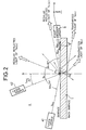
- Fig. 2 is a diagram illustrating a model detecting optical system employed in basic experiments of the present invention.
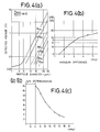
- Fig. 3 shows experimental data indicating different detection voltages of a photoelectric converter element with respect to an extraneous substance having the same particle diameter on the surface or the back surface in the optical system model of Fig. 2 and curves exhibiting the reflection factor and transmittance of a glass substrate.
- Fig. 4 is a diagram illustrating of decision-making conditions for use in deciding the presence of surface and back surface extraneous substances and a preferable range of angles to be set for light projecting and receiving systems according to the present invention.
- Fig. 5 is a diagram illustrating a basic configuration of an optical system in a conventional apparatus for detecting wafer surface flaws.
- Fig. 6 is a diagram illustrating a schematic configuration in a "Method of Detecting Surface Flaws on Liquid Crystal Panel" in the prior art concerning the filed patent application and the principle of separately detecting extraneous substances on both sides.
- Fig. 7 is a diagram illustrating the directivity of scattered light at an extraneous substance in the direction of projection of a laser beam.
- an apparatus 10 for detecting surface extraneous substances on a glass plate has a laser source 41 for generating an S-polarized laser beam T A (s) and a laser source 42 for generating a P-polarized laser beam T B (p) by means of a semiconductor laser element, both the sources being located above a glass substrate 1 as an object under examination such as a liquid crystal panel.
- a light irradiation control circuit 53 drives the laser sources 41, 42 alternately and causes them to generate the S-polarized laser beam T A (s) and P-polarized laser beam T B (p) alternately.
- the light irradiation control circuit 53 is controlled by a decision processing unit 55, which also interlockingly controls the driving of the laser sources and the rotation of a rotary mirror 47.
- the P-polarized laser beam T B (p) has power k times (2 - 4 times) greater than that of the laser beam T A (s).
- the mirror 47 is irradiated with each of the laser beams T A (s), T B (p) via a collimate lens 43, a rotary mirror 44 and a lens 45 and each laser beam is subjected to collimation, angle sweep and focusing commonly and successively via these optical systems. As a result, an optical spot is formed on the surface (pixel formative plane) of the glass plate 1 and used for surface scanning.
- the laser beam T A (s) thus focused is changed in direction by two of the mirrors 461, 462 and projected onto the surface of the glass substrate at a projection angle (elevation angle) of about 20°.
- the laser beam T A (s) is changed in direction by the mirror 47 and projected at a projection angle (elevation angle) of about 70° for scanning the same straight line that is scanned by the laser beam T A (s) on the glass substrate 1.
- the light irradiation control circuit 53 synchronously controls the period of the alternate driving of the laser sources 41, 42 and the rotating speed of the rotary mirror 44 for scanning purposes.
- Scattered light obtainable from scanning at an extraneous substance at the time of laser beam irradiation is received by a light receiving system 5 situated at a reception angle (elevation angle) of about 10° with respect to the surface of the glass substrate 1.
- the scattered light is condensed by a bundle 51 of optical fibers and the light thus condensed is supplied to a photoelectric converter element 52 in which it is converted into an electric signal.
- Detected voltage corresponding to the quantity of light received is produced from the photoelectric converter element 52.
- the detected voltage is divided into detected voltages R A , R B in accordance with the timing at which the driving of the laser source is controlled by the light irradiation control circuit 53 and these voltages are sampled by an A/D converter circuit 4.
- the sampling timing in the A/D converter circuit 54 is controlled by the decision processing unit 55 as well as the light irradiation control circuit 53.
- Each of the detected voltage values resulting from the conversion implemented in the A/D converter circuit 54 correspondingly after laser beam irradiation is read by a microprocessor (MPU) 56 and stored in a memory 57 in the decision processing unit 55.
- the storage operation is performed together with the relevant scanning position (position coordinates on the X- and Y-plane taken on the glass substrate 1) on the glass substrate 1.
- the decision processing unit 55 subsequently executes a predetermined decision processing program to obtain the difference between the detected voltages and decides whether they are equal or which of them is greater.
- the decision processing unit 55 further decides the presence of a surface extraneous substance when both voltages are equal or when one of them is greater. In this case, intended data for use in computing the difference between the voltage values is concerned with what is higher than the noise level.
- the reception angle of the light receiving system 5 is set at about 10°, which is smaller than an angle at which regular reflected light is received from either the first or the second light projecting system.
- the light receiving system receives 5 almost nearly no scattered light.
- the detected voltage values resulting from the reception of light are processed to make them noise levels and only those detected in such a state that extraneous substances are actually detected are taken up for the intended purpose.
- the light receiving system for receiving the scattered light is arranged at a reception angle of about 10° in the forward direction of light reception.
- the quantity of scattered light incident on the light receiving system 5 out of the scattered light in front of the surface extraneous substance due to the laser beam T A (s) is consequently large.
- scattered light in front of the back surface extraneous substance due to the laser beam T A (s) considerably attenuates because of internal reflection within the glass substrate.
- the quantity of transmitting light is generally smaller than that of reflected light in the S-polarized laser beam, scattered light originating from the back surface extraneous substance and entering the light receiving system located on the surface side is small in quantity and therefore the difference between the detected voltages tends to increase.
- the laser beam T A (s) is projected at a projection angle of about 70° from the surface of the glass substrate 1 (20° as viewed from the normal line), whereas the light receiving system 5 for receiving the scattered light is situated at an angle of about 10° from the surface (about 80° as viewed from the normal line), whereby the light receiving system receives light sidewise at an angle of about 100°. Consequently, the scattered light incident on the light receiving system 5 out of the scattered light at the surface and the back surface extraneous substance becomes less intense than what derives from the laser beam T A (s).
- Fig. 3(a) is a graph illustrating such a state as will be described later.
- the voltage detected in the light receiving system 5 with the irradiation of the laser beam T A (s) is represented by R A and what is detected therein with the irradiation of the laser beam T B (p), by R B .
- R A the voltage detected when a surface extraneous substance is detected
- R Ab the voltage detected when a back surface extraneous substance is detected
- Fig. 3 shows it is obtainable from measurement that the detected voltages remain in the above size relation.
- Ps indicates standard particles of various particle diameters sticking to the surface of the glass substrate 1.
- a plurality of standard particles sticking to the surface are made to constitute the surface extraneous substance Ps and then the glass substrate 1 is turned upside down to make the surface extraneous substance a back surface extraneous substance. With this arrangement, the surface and the back surface may be examined in such a state that an extraneous substance of the same variety is sticking to both sides.
- the outputs of the laser beam T A (s) and the laser beam T B (p) are adjusted to be equal.
- the semiconductor laser elements of the laser sources 41, 42 are driven alternately to oscillate under the control of the light irradiation control circuit 53.
- the detected voltages (R As , R Ab ), (R Bs , R Bb ) of scattered light at the extraneous substance on the surface or the back surface side in response to the irradiation of the laser beams T A (s), T B (p) are obtained alternately from the light receiving system 5.
- data shown in Fig. 3(a) was obtained.
- ⁇ A , ⁇ B represent detected voltages corresponding to the logarithmic difference between irregular reflection from the surface and what is from the back surface in response to the irradiation of the laser beams T A (s), T B (p), respectively.
- ⁇ A designates the mean value of the logarithmic difference between the detected voltages R As , R Ab with the irradiation of the laser beam T A (s)
- ⁇ B designates the mean value of the logarithmic difference between the detected voltages R Bs , R Bb with the irradiation of the laser beam T B (s).
- ⁇ A indicates a difference of one digit or greater between the detected voltages
- ⁇ B indicates a difference of less than one digit therebetween.
- the detected voltage R As shows a maximum value at any point as shown in data on each of the particle diameters (3 ⁇ m, 6.4 ⁇ m and 25 ⁇ m).
- the back surface extraneous substance Pb also causes intense forward scattered light, it conforms to the value (1/ ⁇ A as illustrated) of the detected voltage R Ab (marked with O) as it considerably attenuates because of internal reflection within the glass substrate.
- the detected voltages relating to the other particles are substantially arranged in order, the data are considered sufficiently reliable. Then the mean value of those detected voltages is obtained and straight lines of the detected voltages R As , R Bs , R Ab and R Bb are regarded as those indicating representative values.
- Fig. 3(b) shows transmittance curves of polarized light waves with respect to a glass substrate for use in a generally known liquid crystal panel.
- the S-polarized light wave incident at an incident angle ⁇ (°) is reflected from the surface of the glass substrate and the reflection factor of power is indicated with a dotted line of E(s).
- the reflection factor of power of the P-polarized light wave is indicated with E(p).
- the reflection factor of the S-polarized laser beam is greater than that of the P-polarized one with the incident angle ranging from about 20° to about 85° in the case of the glass substrate for use in a liquid crystal panel.
- ⁇ B indicating the logarithmic difference between the detected voltage due to irregular reflection on both sides is smaller than ⁇ A indicating the logarithmic difference likewise.
- ⁇ A and ⁇ B will not become identical even though the transmittance is corrected. This is because the condition of the internal reflection is considered variable, depending on the direction of polarization of the light wave.
- the decision processing unit 55 decides the presence of the surface extraneous substance when R A - R B is is positive in value or when R A /R B is not less than 1; it is needless say acceptable to presume the presence of the back surface extraneous substance from the result in reverse.
- the output of the laser beam T B (p) may be switched selectively in such a way that it becomes k (2 - 4) times greater in intensity than that of laser beam T A (s).
- the laser beam T B (p) is K (2 - 4) times greater in intensity than the laser beam T A (s)
- the detected voltages R Bs , R Bb deriving from the laser beam T B (p) are equally set k times greater.
- the multiple k is very important in the sense that the order of the detected voltage in size is varied as shown in Fig. 4(a).
- the overall operation of the apparatus for detecting a surface extraneous substance on a glass substrate as shown in Fig. 1 comprises the following steps.
- the decision processing unit 55 causes the surface of the glass substrate 1 to be irradiated with the laser beam T A (s) and the laser beam T B (p) having an output k times greater so as to scan the surface of the glass substrate 1 to collect detective voltage R with respect to scattered light in response to the scanning position, so that the respective results are stored in the memory 57.
- MPU 56 obtains the difference between the detected voltages R A , R B with respect to the same scanning position.
- the extraneous substance detected when R A ⁇ R B is designated as what is sticking to the surface (pixel formative plane side) of the glass substrate and what is detected when R A ⁇ R B is designated as a back surface extraneous substance.
- the safety precaution is to side with the surface extraneous substance.
- the process of deciding the presence of such a surface or back surface extraneous substance by means of the decision processing unit 55 may comprise the steps of collecting data on either the detected voltage R A or R B corresponding to respective measurement coordinates on the glass substrate 1 beforehand, storing the resulting data in the memory 57, storing the detected data on the opposite side in the memory 57, and reading the detected data on the detected voltages R A or R B that have been collected correspondingly.
- angles at which two of the light projecting and receiving system are installed only need to basically satisfy Eq. (3) in detection of extraneous substances or flaws.
- a glass substrate for use in a liquid crystal panel roughly ranging from one to several millimeters in thickness, its angle is set in an elevation angle range smaller by about 2° than that of the elevation angle of the light projecting system of the laser beam T A (s) in order for the regular reflected light from the light projecting system of the laser beam T A (s) to be unreceivable.
- the detected voltage whose level exceeds the noise level is generated even though there is no extraneous substance, as shown in the S/N ratio shown in Fig. 4(b), when the difference between the elevation angle of the light receiving system and those of projecting systems decreases to 2° or less.
- the extraneous substance detection level on the back surface side is lower than that on the surface side. Consequently, the back surface extraneous substance S/N ratio that has been taken reveals the fact that, as shown in Fig. 4(c) illustrating the S/N ratio in the characteristics of (R As /R Bs ) x (R Bb /R Ab ), the irregular reflection from the back surface of the glass substrate exceeds the noise level and is received if the light receiving system is situated at an angle of 5° or greater even when there exists no back surface extraneous substance.
- the elevation angle of the light receiving system should preferably substantially range from 5° to 15°.
- the light projecting system of the laser beam T A (s) it is preferred for the light projecting system of the laser beam T A (s) to be angled at 7° or larger.
- the maximum incident angle of the light projecting system responsive to the laser beam T A (s) becomes 25° and its elevation angle is set at 75°.
- the difference in elevation angle between the light projecting systems relating to the respective laser beams T A (s), T B (p) should be not less than 50° to make the difference between the detected voltages R A and R B about one digit or greater in responsive to the irradiation of the laser beam T A (s). Therefore, the angle of the light projecting system relating to the laser beam T A (s) should be set at not less than 20°.
- the angle of light projecting system relating to the laser beam T A (s) should preferably range from 7° to 25°, whereas what relates to the laser beam T B (p) should preferably range from 57° to 75°.
- the more preferable range empirically considered is such that the light receiving system should be provided at an elevation angle of about 10° ⁇ 3° perpendicular to the surface. Any extraneous substance may be detected in such a preferable state as what is understood in reference to the angle setting shown in the embodiment above, wherein with respect to the projection angle of the laser beam T A (s), it is set at an elevation angle of about 20° ⁇ 3° and with respect to that of the laser beam T B (p), it is set at an elevation angle of about 70° ⁇ 3°.
Landscapes
- Physics & Mathematics (AREA)
- Health & Medical Sciences (AREA)
- Life Sciences & Earth Sciences (AREA)
- Chemical & Material Sciences (AREA)
- Analytical Chemistry (AREA)
- Biochemistry (AREA)
- General Health & Medical Sciences (AREA)
- General Physics & Mathematics (AREA)
- Immunology (AREA)
- Pathology (AREA)
- Investigating Materials By The Use Of Optical Means Adapted For Particular Applications (AREA)
- Length Measuring Devices By Optical Means (AREA)
Description
- The present invention relates generally to apparatus for detecting extraneous substances on glass plates and more particularly to an apparatus for detecting extraneous substances on a glass plate so that when extraneous substances are sticking to the surface and the back surface of the glass plate, the extraneous substance sticking to the surface thereof can be separated from what is sticking to the back surface before being detected.
- Flaw inspecting apparatus are generally used for detecting extraneous substances sticking to the surfaces of masking substrates (glass substrates) and silicon wafers for use in manufacturing semiconductor ICs, and glass plates for use in liquid crystal panels and the like, the extraneous substances ordinarily including flaws such as defects of their surfaces themselves. Product quality is thus maintained at not lower than a certain level.
- Fig. 5 shows a basic configuration of a flaw detecting optical system in an apparatus for detecting wafer surface flaws as a flaw inspecting apparatus of the sort described above by way of example. The optical system consists of a light projecting and a
light receiving system laser beam source 21 are focused by alight projecting lens 22. An optical spot is formed on the surface of awafer plate 1 as an object under examination. When the optical spot scans the surface of thewafer plate 1 under a revolving scanning or XY scanning method, it will be scattered at a place where a flaw is found. The scattered light is condensed by acondenser lens 31 in thelight receiving system 3 and received by alight receiver 32. A flaw detection signal is thus obtained. Astopper 33 provided in thelight receiving system 3 is inserted for improving the S/N ratio by cutting off the regular reflected light deriving from the laser beam. - With the basic configuration described above, various improvements have been introduced in light projecting and light receiving systems in not only optical systems for detecting wafer surface flaws but also those for detecting flaws on masking substrates, glass plates for use in liquid crystal panels and the like. For instance, it is commonly practiced to improve the condensation effect by means of optical fibers instead of the
condenser lens 31 as a light receiving system. - A TFT-type liquid crystal panel is formed with an extra-fine liquid crystal pixel electrode and a film transistor (TFT), these being formed by etching on the surface of a glass plate. The surface of the glass plate (glass substrate) with the liquid crystal pixel electrode and TFT formed thereon is provisionally called a pixel formative plane, for instance. With extraneous substances sticking to the pixel formative plane, it is highly probable for a number of TFTs connected to each other to simultaneously malfunction. The extraneous substances sticking to that surface may seriously affect the quality of the liquid crystal panel as a product; this makes it necessary to use such a flaw detecting optical system for examining the presence or absence of extraneous substances on the pixel formative plane of the glass substrate.
- Incidentally, the glass substrate having a pixel formative plane is a plate which is translucent, as thin as about 1 mm and has high transmittance. Consequently, the problem is that extraneous substances sticking to the pixel formative plane (hereinafter simply called 'surface extraneous substance(s)') and those sticking to the back surface of the glass substrate (hereinafter simply called 'back surface extraneous substance(s)') may simultaneously be detected. The back surface of the glass substrate is normally used as a side where an image to be displayed is observed or where back light is transmitted therethrough when the glass substrate is assembled as part of a liquid crystal panel. This means the back surface of the glass substrate is only needed to be a glass surface and as far as extraneous substances sticking thereto are minute, they pose no problems; in other words, the extraneous substances are not regarded as flaws in many cases. In case these extraneous substances are detected as flaws, the good parts are assumed the bad and the yield of parts tends to decrease, thus resulting in a heavy loss.
- While the operation of detecting flaws on a glass substrate for a liquid crystal display panel is performed, only extraneous substances on a pixel formative plane on the surface side thereof as viewed from liquid crystal are detected so that those on the back surface side may be ignored. However, the fact that the glass substrate is a thin plate having high transmittance makes it actually difficult to detect extraneous substances on the surface and the back surface thereof separately.
- Present inventors proposed the art of detecting extraneous substances on both sides separately and the present applicants filed an application for a patent under the title "A Method of Detecting Surface Flaws on Liquid Crystal Panel", Japanese Patent Application No. 327966/1989, dated Dec. 18, 1989. Referring to Figs. 6(a), 6(b), a general description will subsequently be given of the method.
- As shown in Fig. 6(a), a pair of light projecting and
receiving systems glass substrate 1 as an object under examination, whereas a pair of light projecting and receiving systems 2', 3' are provided symmetrically about theglass substrate 1 on the back surface side thereof. Laser beams T, T' of substantially the same intensity are used respectively to form optical spots on the surface and the back surface, whereby alternate scanning is implemented. On the assumption that the sensitivity of both twolight receiving systems 3, 3' is substantially identical, the detected signals of scattered light are compared. Of the detected signals in thelight receiving system 3 on the surface side after the comparison is made, what is greater than the detected signal in the light receiving system 3' on the back surface side is defined as a flaw detecting signal concerning an extraneous substance, including a flaw, sticking to the surface. - A description will subsequently given of the basic principle of making the above decision accordingly. Fig. 6(b) refers to cases where an extraneous substance Ps is sticking to the surface of the
glass substrate 1 and where an extraneous substance Pb is sticking to the back surface thereof. In these cases, thelight receiving system 3 on the surface side directly receives scattered light Rs deriving from the laser beam T at the surface extraneous substance Ps and simultaneously irregular reflected light at the extraneous substance Pb on the back surface side. In other words, scattered light Rb at the extraneous substance Pb on the back surface side passes through theglass substrate 1 and reaches thelight receiving system 3. Due to total reflection, the scattered light Rb attenuates as it passes through theglass substrate 1. As a result, the extraneous substance Ps on the surface side imparts to thelight receiving system 3 scattered light more intense than what is directed to the light receiving system 3' on the back surface side. - Such is also the case with the extraneous substance on the back surface side. The light receiving system 3' on the back surface side directly receives scattered light Rb' deriving from the laser beam T' at the extraneous substance Pb on the back surface side and simultaneously irregular reflected light at the extraneous substance Ps on the surface side likewise. In other words, scattered light Rs' at the surface extraneous substance Ps passes through the
glass substrate 1 and reaches the light receiving system 3'. The scattered light Rs' also attenuates as it passes through theglass substrate 1. The extraneous substance Pb on the back surface side imparts to the light receiving system 3' scattered light more intense than what is directed to thelight receiving system 3 on the surface side. - A comparison of the detected signals on both sides to find which one of the
light receiving systems 3, 3' is receiving light more intense than the other makes it possible to determine whether the extraneous substance in question is located on the surface or the back surface side. - However, it has also frequently occurred that an extraneous substance on the surface side still remains inseparable from what exists on the back surface side when the above decision-making principle is actually applied and this has posed a problem. Since any apparatus using such decision-making principle requires installing both light projecting and receiving systems on respective sides of an object under examination, the apparatus has proved unfavorable in view of its maintenance and the like as it tends to increase in size.
- The present inventors have primarily given it careful consideration why respective extraneous substances on the surface and back surface sides are left inseparable when the above decision-making principle is actually applied and reasoned that the principle is based on a tacit understanding that the directivity of scattered light at the extraneous substance is uniform and omnidirectional. Referring to Figs. 7(a), 7(b), a description will be given of this problem. Fig. 7 shows the results of experiments made on the directivity of scattered light at an extraneous substance. As shown in Fig. 7(a), the intensity of scattered light R at an extraneous substance P in the direction of an angle ε from the direction of projection of a laser beam T is considered first. Fig. 7(b) shows experimental results by way of example. More specifically, Fig. 7(b) shows curves of the intensity F of scattered light at the angle ε(°) with the particle diameter as a parameter (1 - 10 µm). The intensity F of the scattered light drastically varies with the angle ε. The intensity F of the scattered light is extremely great in the vicinity of an angle ε = 0°, that is, in the direction of projection (forward). When the particle diameter is 1 µm, for instance, the intensity is about 150 times greater in the direction of 90° (sideward). When the particle diameter is 10 µm, it is greater by about three digits in the direction of 90° (sideward). By this is meant that when the surface of a glass substrate is irradiated with the laser beam at an angle, the directivity is such that scattering at the angle ε = 0°, that is, forward scattering is seen to be intense.
- In consideration of the forward directivity, the decision-making principle is appraised on the assumption that a
light receiving system 3 has an angle as shown in Fig. 6(a). Referring to Fig. 6(b), forward scattered light deriving from a laser beam T' and undergoing total reflection within aliquid crystal panel 1, rather than scattered light Rs deriving from the laser beam T at a surface extraneous substance Ps, may be received more intensely by thelight receiving system 3. The forward scattered light deriving from the laser beam T, rather than scattered light Rb' deriving from the laser beam T' at an extraneous substance Pb on the back surface, may likewise be received more intensely by a light receiving system 3'. Therefore, it will be understood to be not always appropriate that a decision is made by simply comparing the sizes of the signals detected by both light receiving systems so as to separate the extraneous substances Ps, Pb. In Fig. 6(a), projection angles of respectivelight projecting systems 2, 2' and reception angles of the respectivelight receiving systems 3, 3' have not been specified. - In the present invention, special attention has been directed to the fact that there exist sturdy directivity in front of such scattered light and consequently not only the optimum arrangement of light projecting and receiving systems but also optimum angles of projection and reception. The optimum configuration that has been contrived herein comprises the provision of such light projecting and receiving systems on one side where a pixel formative plane is formed accordingly, so that extraneous substances on the surface and the back surface are separately detected.
- More specifically, an apparatus for detecting extraneous substances on a glass plate according to the present invention is as according to
claim 1. In this case, the presence of an extraneous substance on the surface is ultimately decided when a signal level obtainable in the light receiving system in response to the irradiation of the S-polarized laser beam is higher than a signal level obtainable in the light receiving system in response to the irradiation of the P-polarized laser beam. - The specific relation described above refers to a case where the output level of the P-polarized laser beam is set in such a way that a third and a fourth detection level are held between a first and a second detection level wherein when an extraneous substance having a certain particle diameter on the surface is irradiated with the S-polarized laser beam, the level of the scattered light detected by the light receiving system is defined as the first detection level, wherein when the extraneous substance is irradiated with the S-polarized laser beam via the glass plate with its surface down, the level of the scattered light detected by the light receiving system is defined as the second detection level, wherein when the extraneous substance is irradiated with the P-polarized laser beam, the level of the scattered light detected by the light receiving system is defined as the third detection level, and wherein when the extraneous substance is irradiated with the P-polarized laser beam via the glass plate with its surface down, the level of the scattered light detected by the light receiving system is defined as the fourth detection level.
- Incidentally, it is needed to determine the presence of the extraneous substance, including a flaw, on the back surface only when the signal level obtainable in the light receiving system in response to the irradiation of the laser beam from the first light projecting system is lower than what is obtainable in the light receiving system in according with the irradiation of the laser beam from the second light projecting system.
- In the case of an apparatus for detecting an extraneous substance, including a flaw, on the surface of a glass substrate for a liquid crystal panel, two of the first and second light projecting systems should preferably be provided above and opposite to the surface (pixel formative plane) of the glass substrate at the following angles: A light receiving system should be provided at a reception angle of about 10° to the surface. Then the first light projecting system should be set at an elevation angle of about 20° as a projection angle and the second light projecting system at an elevation angle of about 7° as a projection angle. Moreover, the laser beam power of the second light projecting system is set in the range of 2 - 4 with respect to the irradiation power of the laser beam of the first light projecting system.
- Therefore, an object of the present invention is to provide such an apparatus for detecting extraneous substances on a glass plate that has light projecting systems and a light receiving system on one side of the glass plate and is capable of detecting an extraneous substance on either the surface or the back surface of the glass plate separately from what is on the other.
- Another object of the present invention is to provide such an apparatus for detecting extraneous substances on a glass plate that has light projecting systems and a light receiving system on one side of the glass plate and is capable of detecting an extraneous substance on the surface of the glass plate separately from what is on the back surface thereof.
- Still another object of the present invention is to provide such an apparatus for detecting extraneous substances on a glass substrate that has light projecting systems and a light receiving system above a pixel formative plane and is capable of detecting an extraneous substance on the pixel formative plane side of the glass substrate for use in a liquid crystal panel separately from what is on the back surface side thereof.
- A further object of the present invention is to provide such an apparatus for detecting flaws of a glass plate that has light projecting systems and a light receiving system on one side of the glass plate and is capable of detecting a flaw on the surface side of the glass plate separately from what is on the back surface side thereof.
- Fig. 1 is a diagram illustrating a configuration of an apparatus for detecting extraneous substances on the surface of a glass plate according to the present invention.
- Fig. 2 is a diagram illustrating a model detecting optical system employed in basic experiments of the present invention.
- Fig. 3 shows experimental data indicating different detection voltages of a photoelectric converter element with respect to an extraneous substance having the same particle diameter on the surface or the back surface in the optical system model of Fig. 2 and curves exhibiting the reflection factor and transmittance of a glass substrate.
- Fig. 4 is a diagram illustrating of decision-making conditions for use in deciding the presence of surface and back surface extraneous substances and a preferable range of angles to be set for light projecting and receiving systems according to the present invention.
- Fig. 5 is a diagram illustrating a basic configuration of an optical system in a conventional apparatus for detecting wafer surface flaws.
- Fig. 6 is a diagram illustrating a schematic configuration in a "Method of Detecting Surface Flaws on Liquid Crystal Panel" in the prior art concerning the filed patent application and the principle of separately detecting extraneous substances on both sides.
- Fig. 7 is a diagram illustrating the directivity of scattered light at an extraneous substance in the direction of projection of a laser beam.
- As shown in Fig. 1, an
apparatus 10 for detecting surface extraneous substances on a glass plate has alaser source 41 for generating an S-polarized laser beam TA(s) and alaser source 42 for generating a P-polarized laser beam TB(p) by means of a semiconductor laser element, both the sources being located above aglass substrate 1 as an object under examination such as a liquid crystal panel. A lightirradiation control circuit 53 drives thelaser sources irradiation control circuit 53 is controlled by adecision processing unit 55, which also interlockingly controls the driving of the laser sources and the rotation of arotary mirror 47. In this case, the P-polarized laser beam TB(p) has power k times (2 - 4 times) greater than that of the laser beam TA(s). Themirror 47 is irradiated with each of the laser beams TA(s), TB(p) via acollimate lens 43, arotary mirror 44 and alens 45 and each laser beam is subjected to collimation, angle sweep and focusing commonly and successively via these optical systems. As a result, an optical spot is formed on the surface (pixel formative plane) of theglass plate 1 and used for surface scanning. The laser beam TA(s) thus focused is changed in direction by two of themirrors mirror 47 and projected at a projection angle (elevation angle) of about 70° for scanning the same straight line that is scanned by the laser beam TA(s) on theglass substrate 1. The lightirradiation control circuit 53 synchronously controls the period of the alternate driving of thelaser sources rotary mirror 44 for scanning purposes. - Scattered light obtainable from scanning at an extraneous substance at the time of laser beam irradiation is received by a
light receiving system 5 situated at a reception angle (elevation angle) of about 10° with respect to the surface of theglass substrate 1. The scattered light is condensed by abundle 51 of optical fibers and the light thus condensed is supplied to aphotoelectric converter element 52 in which it is converted into an electric signal. Detected voltage corresponding to the quantity of light received is produced from thephotoelectric converter element 52. The detected voltage is divided into detected voltages RA, RB in accordance with the timing at which the driving of the laser source is controlled by the lightirradiation control circuit 53 and these voltages are sampled by an A/D converter circuit 4. The sampling timing in the A/D converter circuit 54 is controlled by thedecision processing unit 55 as well as the lightirradiation control circuit 53. - Each of the detected voltage values resulting from the conversion implemented in the A/
D converter circuit 54 correspondingly after laser beam irradiation is read by a microprocessor (MPU) 56 and stored in amemory 57 in thedecision processing unit 55. The storage operation is performed together with the relevant scanning position (position coordinates on the X- and Y-plane taken on the glass substrate 1) on theglass substrate 1. Thedecision processing unit 55 subsequently executes a predetermined decision processing program to obtain the difference between the detected voltages and decides whether they are equal or which of them is greater. Thedecision processing unit 55 further decides the presence of a surface extraneous substance when both voltages are equal or when one of them is greater. In this case, intended data for use in computing the difference between the voltage values is concerned with what is higher than the noise level. - In this embodiment, the reception angle of the
light receiving system 5 is set at about 10°, which is smaller than an angle at which regular reflected light is received from either the first or the second light projecting system. When neither the surface nor the back surface has an extraneous substance, the light receiving system receives 5 almost nearly no scattered light. However, as thelight receiving system 5 may still receive some scattered or disturbed light from the back surface side even when no extraneous substances exist on both sides, the detected voltage values resulting from the reception of light are processed to make them noise levels and only those detected in such a state that extraneous substances are actually detected are taken up for the intended purpose. - When the outputs of the laser beams TA(s), TB(p) are assumed equal, with the detection optical system configuration above, the following relation is established.
- While the laser beam TA(s) is projected onto the surface of the glass substrate at a projection angle of about 20° in the embodiment shown, the light receiving system for receiving the scattered light is arranged at a reception angle of about 10° in the forward direction of light reception. The quantity of scattered light incident on the
light receiving system 5 out of the scattered light in front of the surface extraneous substance due to the laser beam TA(s) is consequently large. On the other hand, scattered light in front of the back surface extraneous substance due to the laser beam TA(s) considerably attenuates because of internal reflection within the glass substrate. Moreover, since the quantity of transmitting light is generally smaller than that of reflected light in the S-polarized laser beam, scattered light originating from the back surface extraneous substance and entering the light receiving system located on the surface side is small in quantity and therefore the difference between the detected voltages tends to increase. - With respect to the light projecting
system 4, the laser beam TA(s) is projected at a projection angle of about 70° from the surface of the glass substrate 1 (20° as viewed from the normal line), whereas thelight receiving system 5 for receiving the scattered light is situated at an angle of about 10° from the surface (about 80° as viewed from the normal line), whereby the light receiving system receives light sidewise at an angle of about 100°. Consequently, the scattered light incident on thelight receiving system 5 out of the scattered light at the surface and the back surface extraneous substance becomes less intense than what derives from the laser beam TA(s). Fig. 3(a) is a graph illustrating such a state as will be described later. - The voltage detected in the
light receiving system 5 with the irradiation of the laser beam TA(s) is represented by RA and what is detected therein with the irradiation of the laser beam TB(p), by RB. With the irradiation of the laser beam TA(s), further, the voltage detected when a surface extraneous substance is detected is represented by RAs (the accompanying s means the surface extraneous substance) and the voltage detected when a back surface extraneous substance is detected, by RAb (the accompanying b means the back surface extraneous substance). With the irradiation of the laser beam TB(p) likewise, the voltage detected when a surface extraneous substance is detected is represented by RBs and the voltage detected when a back surface extraneous substance is detected, by RBb. Assuming the light irradiation power of the laser beam TA(s) and the laser beam TB(p) directed to the surface of theglass substrate 1 is equal, the following relation is established among the detected voltages when the order of their intensity is considered:

- However, these are related to each other in substantially the same way even if RAs/RAs and RBs/RBb ratios are chosen for use.
- Fig. 3 shows it is obtainable from measurement that the detected voltages remain in the above size relation.
- In Fig. 2, Ps indicates standard particles of various particle diameters sticking to the surface of the
glass substrate 1. A plurality of standard particles sticking to the surface are made to constitute the surface extraneous substance Ps and then theglass substrate 1 is turned upside down to make the surface extraneous substance a back surface extraneous substance. With this arrangement, the surface and the back surface may be examined in such a state that an extraneous substance of the same variety is sticking to both sides. The S-polarized laser beam TA(s) is projected from thelaser source 41 provided above the glass substrate at a projection angle of 18° (incident angle Θa = 72°) in the direction perpendicular to the surface of theglass substrate 1. Moreover, the P-polarised laser beam TB(p) is projected from thelaser source 42 at a projection angle of 70° (incident angle Θb = 20°) in the direction perpendicular to the surface thereof. In this case, the outputs of the laser beam TA(s) and the laser beam TB(p) are adjusted to be equal. Further, the semiconductor laser elements of thelaser sources irradiation control circuit 53. - As an example of the case with an angle of 10°, the
light receiving system 5 is provided in the direction of 8° (reflection angle Θr = 82°) perpendicular to the surface of the glass substrate. The detected voltages (RAs, RAb), (RBs, RBb) of scattered light at the extraneous substance on the surface or the back surface side in response to the irradiation of the laser beams TA(s), TB(p) are obtained alternately from thelight receiving system 5. As the detected voltages at that time, data shown in Fig. 3(a) was obtained. In this case, ρA, ρB represent detected voltages corresponding to the logarithmic difference between irregular reflection from the surface and what is from the back surface in response to the irradiation of the laser beams TA(s), TB(p), respectively. In other words, ρA designates the mean value of the logarithmic difference between the detected voltages RAs, RAb with the irradiation of the laser beam TA(s), whereas ρB designates the mean value of the logarithmic difference between the detected voltages RBs, RBb with the irradiation of the laser beam TB(s). As illustrated, ρA indicates a difference of one digit or greater between the detected voltages, whereas ρB indicates a difference of less than one digit therebetween. - Since the surface extraneous substance Ps with the irradiation of the laser beam TA(s) causes intense forward scattered light as shown in Fig. 3, the detected voltage RAs (marked with X) shows a maximum value at any point as shown in data on each of the particle diameters (3 µm, 6.4 µm and 25 µm). Although the back surface extraneous substance Pb also causes intense forward scattered light, it conforms to the value (1/ρA as illustrated) of the detected voltage RAb (marked with O) as it considerably attenuates because of internal reflection within the glass substrate. In the case of the laser beam TB(p), on the other hand, it is received sidewise as the light receiving system is situated at an angle of 102° (= Θb + Θr) in the direction of projection. For this reason, directivity relating to the intensity of scattered light stays in a weak region and this results in the detected voltage RBs (marked with O) lower than the detected voltage RAs (marked with X). Moreover, the detected voltage RBb (marked with △) becomes lower by 1/ρB than the detected voltage RBs (marked with †) because of internal reflection within the
glass substrate 1. The plurality of particles are tested and the results marked with symbol * (25 µm) designate detected voltage relating to one and the same particle. As the detected voltages relating to the other particles are substantially arranged in order, the data are considered sufficiently reliable. Then the mean value of those detected voltages is obtained and straight lines of the detected voltages RAs, RBs, RAb and RBb are regarded as those indicating representative values. - If the transmittance of the
glass substrate 1 and the influence of the internal reflection are then identical with respect to the laser beams TA(s), TB(p), straight line ratios RAs/RAb = ρA and RBs/RBb = ρB should be identical. However, the actual values ρA ≒ 17, ρB ≒ 6 differ from each other. The main reason for this is that the laser beams TA(s), TB(p) are considered an S-polarized and a P-polarised light wave. - Fig. 3(b) shows transmittance curves of polarized light waves with respect to a glass substrate for use in a generally known liquid crystal panel. First, the S-polarized light wave incident at an incident angle Θ(°) is reflected from the surface of the glass substrate and the reflection factor of power is indicated with a dotted line of E(s). On the other hand, the reflection factor of power of the P-polarized light wave is indicated with E(p). No-reflection occurs in the vicinity of the Brewster's angle (57° when n = 1.5) determined by the refractive index n of the glass substrate. Consequently, the characteristics of both curves differ from each other. In view of this, the reflection factor of the S-polarized laser beam is greater than that of the P-polarized one with the incident angle ranging from about 20° to about 85° in the case of the glass substrate for use in a liquid crystal panel.
- In consideration of the fact that transmitted light in the glass substrate is reflected twice from the surface and the back surface, on the other hand, power transmittance curves D(s), D(p) are obtained from the S-polarized and the P-polarized light wave. When the laser beams TA(s), TB(p) are applied to these curves, the laser beam TA(s) is such that the transmittance of the P-polarized laser beam is greater than that of the S-polarized laser beam with the incident angle ranging from about 20° to about 85°. The transmittance of the laser beam TA(s) in the preceding example of Θa = 72° is about 44%, whereas the transmittance of the laser beam TB(p) in the preceding example of Θb = 20° is about 94%. This explains why ρB indicating the logarithmic difference between the detected voltage due to irregular reflection on both sides is smaller than ρA indicating the logarithmic difference likewise. However, ρA and ρB will not become identical even though the transmittance is corrected. This is because the condition of the internal reflection is considered variable, depending on the direction of polarization of the light wave.
- Now assuming the power of laser beam TB(p) is set k (= 3) times greater than that of the laser beam TA(s) as shown in Fig. 1, the straight line RBs, RBb of Fig. 3(a) are increased by k times and moved from a dotted line position to an actual line one as shown in Fig. 4(a). The order of intensity of the respective straight lines then satisfies the following equation:

- RAs > kRBs is derived from the above equation as the condition of deciding the presence of the surface extraneous substance and RAb < kRBb as the condition of deciding the presence of the back surface extraneous substance. Therefore, the presence of either one may be decided by comparing the detected voltages RA, RB in size. Although it is inconceivable to decide the presence of either one when RA = RB, the safety precaution is to side with the surface extraneous substance.
- In this way, the
decision processing unit 55 decides the presence of the surface extraneous substance when RA - RB is is positive in value or when RA/RB is not less than 1; it is needless say acceptable to presume the presence of the back surface extraneous substance from the result in reverse. - In this
apparatus 10 for detecting a surface extraneous substance on a glass substrate, the output of the laser beam TB(p) may be switched selectively in such a way that it becomes k (2 - 4) times greater in intensity than that of laser beam TA(s). As the laser beam TB(p) is K (2 - 4) times greater in intensity than the laser beam TA(s), the detected voltages RBs, RBb deriving from the laser beam TB(p) are equally set k times greater. The multiple k is very important in the sense that the order of the detected voltage in size is varied as shown in Fig. 4(a). - The overall operation of the apparatus for detecting a surface extraneous substance on a glass substrate as shown in Fig. 1 comprises the following steps. The
decision processing unit 55 causes the surface of theglass substrate 1 to be irradiated with the laser beam TA(s) and the laser beam TB(p) having an output k times greater so as to scan the surface of theglass substrate 1 to collect detective voltage R with respect to scattered light in response to the scanning position, so that the respective results are stored in thememory 57. Subsequently,MPU 56 obtains the difference between the detected voltages RA, RB with respect to the same scanning position. In consideration of the order of the size above, the extraneous substance detected when RA ≥ RB is designated as what is sticking to the surface (pixel formative plane side) of the glass substrate and what is detected when RA < RB is designated as a back surface extraneous substance. However, as it is inconceivable to decide the presence of either one when RA = RB, the safety precaution is to side with the surface extraneous substance. - The process of deciding the presence of such a surface or back surface extraneous substance by means of the
decision processing unit 55 may comprise the steps of collecting data on either the detected voltage RA or RB corresponding to respective measurement coordinates on theglass substrate 1 beforehand, storing the resulting data in thememory 57, storing the detected data on the opposite side in thememory 57, and reading the detected data on the detected voltages RA or RB that have been collected correspondingly. - As set forth above, the angles at which two of the light projecting and receiving system are installed only need to basically satisfy Eq. (3) in detection of extraneous substances or flaws. In consideration of not only noise but also scattered light from the back surface side of the glass, it would be necessary to examine the angles of the light projecting and receiving systems for the laser beam TA(s) as ranges for eliminating noise resulting from the reception of scattered light and the like from the back surface side and obtaining detected voltages effective in making a decision. With a glass substrate for use in a liquid crystal panel roughly ranging from one to several millimeters in thickness, its angle is set in an elevation angle range smaller by about 2° than that of the elevation angle of the light projecting system of the laser beam TA(s) in order for the regular reflected light from the light projecting system of the laser beam TA(s) to be unreceivable. At the angle of the light receiving system as an output level free from noise, the detected voltage whose level exceeds the noise level is generated even though there is no extraneous substance, as shown in the S/N ratio shown in Fig. 4(b), when the difference between the elevation angle of the light receiving system and those of projecting systems decreases to 2° or less.
- Moreover, the extraneous substance detection level on the back surface side is lower than that on the surface side. Consequently, the back surface extraneous substance S/N ratio that has been taken reveals the fact that, as shown in Fig. 4(c) illustrating the S/N ratio in the characteristics of (RAs/RBs) x (RBb/RAb), the irregular reflection from the back surface of the glass substrate exceeds the noise level and is received if the light receiving system is situated at an angle of 5° or greater even when there exists no back surface extraneous substance. If the light receiving system is situated at an angle exceeding 16°, the detected output on the back surface side becomes excessive when any extraneous substance exists on the back surface and a value of (RAs/RBs) x (RBb/RAb) decreases to 1.5 or less, thus making it difficult to separate both sides from each other. The elevation angle of the light receiving system should preferably substantially range from 5° to 15°. As a result, it is preferred for the light projecting system of the laser beam TA(s) to be angled at 7° or larger. As shown in Fig. 7(b), an effective light detecting angle ranges up to about ∠ε = 100 in the forward direction of the light projecting system. Therefore, the maximum incident angle of the light projecting system responsive to the laser beam TA(s) becomes 25° and its elevation angle is set at 75°. Like the embodiment shown, moreover, the difference in elevation angle between the light projecting systems relating to the respective laser beams TA(s), TB(p) should be not less than 50° to make the difference between the detected voltages RA and RB about one digit or greater in responsive to the irradiation of the laser beam TA(s). Therefore, the angle of the light projecting system relating to the laser beam TA(s) should be set at not less than 20°. In other words, the angle of light projecting system relating to the laser beam TA(s) should preferably range from 7° to 25°, whereas what relates to the laser beam TB(p) should preferably range from 57° to 75°.
- In the case of a glass substrate for use in a liquid crystal panel about 1 mm thick, the more preferable range empirically considered is such that the light receiving system should be provided at an elevation angle of about 10° ± 3° perpendicular to the surface. Any extraneous substance may be detected in such a preferable state as what is understood in reference to the angle setting shown in the embodiment above, wherein with respect to the projection angle of the laser beam TA(s), it is set at an elevation angle of about 20° ± 3° and with respect to that of the laser beam TB(p), it is set at an elevation angle of about 70° ± 3°.
Claims (9)
- An apparatus for detecting extraneous substance on a glass plate, comprisinga first light projecting system (41, 461, 462) for irradiating the surface of the glass plate (1) with an S-polarized laser beam at a first elevation angle, as viewed from the surface,a second light projecting system (42, 47) for irradiating the surface under examination with a P-polarized laser beam at a second elevation angle greater than the first elevation angle, anda light receiving system (5) for receiving light scattered from the surface under examination at a third elevation angle smaller than the first elevation angle, the light receiving system being arranged in a direction opposite to the direction of irradiation with a normal line set up at the beam irradiation point therebetween,wherein a first intensity level of detected light signal is used when an extraneous substance on the surface under examination is irradiated with an S-polarized beam, a second intensity level of detected light signal is used when the extraneous substance is irradiated with the S-polarized beam through the glass substrate, with the glass plate being turned upside down, a third intensity level of detected light signal is used when the extraneous substance is irradiated with the P-polarized beam, and a fourth intensity level of detected light signal is used when the extraneous substance is irradiated with the P-polarized beam through the glass plate, with the glass plate turned upside down, andwherein the output intensity level of the P-polarized beam is set so that the intensity levels of the detected light signals are in order of increasing value the fourth, the second, the third and the first.
- The apparatus of claim 1, wherein when the signal level obtained by the light receiving system corresponding to the irradiation with the S-polarized beam is greater than that obtained from the corresponding irradiation with the P-polarized beam, the extraneous substance is judged as existing on the surface under examination.
- The apparatus of claim 1 or 2, wherein when the signal level obtained by the light receiving system corresponding to the irradiation with the P-polarized beam is greater than that obtained from the corresponding irradiation with the S-polarized beam, the extraneous substance is judged as existing on the back surface under examination.
- The apparatus of any of claims 1 to 3, wherein the output of the beam from the second light projecting system (42, 47) is from two to four times greater than that from the first light projecting system (41, 461, 462).
- The apparatus of any of claims 1 to 4, wherein the glass plate (1) is a glass substrate for use in a liquid crystal panel, and wherein the first elevation angle ranges from 7° to 25°, the second elevation angle from 57° to 75°, and the third elevation angle from 5° to 15°.
- The apparatus of claim 4, wherein the difference between the first and second elevation angles is equal to or greater than 50°.
- The apparatus of claim 6, wherein the first elevation angle is from 17° to 23°, preferably about 18°, the second elevation angle is 67° to 73°, preferably about 70°, and the third elevation angle is 7° to 13°, preferably about 8°.
- The apparatus of claim 7, wherein said glass substrate (1) is about 1 mm thick and an electrode for liquid crystal display is formed on the surface under examination.
- The apparatus of any of claims 1 to 8, wherein the extraneous substance is a flaw in the glass plate (1).
Applications Claiming Priority (2)
| Application Number | Priority Date | Filing Date | Title |
|---|---|---|---|
| JP414979/90 | 1990-12-27 | ||
| JP41497990 | 1990-12-27 |
Publications (3)
| Publication Number | Publication Date |
|---|---|
| EP0493815A2 EP0493815A2 (en) | 1992-07-08 |
| EP0493815A3 EP0493815A3 (en) | 1992-10-14 |
| EP0493815B1 true EP0493815B1 (en) | 1996-03-06 |
Family
ID=18523394
Family Applications (1)
| Application Number | Title | Priority Date | Filing Date |
|---|---|---|---|
| EP91122311A Expired - Lifetime EP0493815B1 (en) | 1990-12-27 | 1991-12-27 | Apparatus for detecting extraneous substance on glass plate |
Country Status (5)
| Country | Link |
|---|---|
| US (1) | US5245403A (en) |
| EP (1) | EP0493815B1 (en) |
| JP (1) | JP2671241B2 (en) |
| KR (1) | KR0159290B1 (en) |
| DE (1) | DE69117714T2 (en) |
Cited By (1)
| Publication number | Priority date | Publication date | Assignee | Title |
|---|---|---|---|---|
| US10634555B2 (en) | 2018-04-18 | 2020-04-28 | Xenon Corporation | Protecting a UV-transmissive window |
Families Citing this family (42)
| Publication number | Priority date | Publication date | Assignee | Title |
|---|---|---|---|---|
| JP3259331B2 (en) * | 1992-05-29 | 2002-02-25 | キヤノン株式会社 | Surface condition inspection device |
| JPH0682239A (en) * | 1992-09-04 | 1994-03-22 | Matsushita Electric Ind Co Ltd | Method and apparatus for measuring pretilt angle of liquid crystal material |
| DE4300169A1 (en) * | 1993-01-07 | 1994-07-14 | Alfill Getraenketechnik | Method and device for testing bottles |
| ES2076083B1 (en) * | 1993-06-04 | 1996-06-01 | Fuesca Sl | APPARATUS AND METHOD OF MEASURING AND CONTROLLING THE DENSITY OF RETICULATION OF THE HOT AND COLD TREATMENTS OF LIGHT GLASS. |
| JPH07190942A (en) * | 1993-12-24 | 1995-07-28 | Nec Corp | Equipment for inspecting dust particle on mirror surface |
| JPH07209202A (en) * | 1994-01-21 | 1995-08-11 | Canon Inc | Surface state inspection equipment, exposure apparatus employing it, and production of device using the exposure apparatus |
| US6271916B1 (en) * | 1994-03-24 | 2001-08-07 | Kla-Tencor Corporation | Process and assembly for non-destructive surface inspections |
| US5412221A (en) * | 1994-04-26 | 1995-05-02 | The United States Of America As Represented By The Administrator Of The National Aeronautics And Space Administration | Particle fallout/activity sensor |
| US5903342A (en) * | 1995-04-10 | 1999-05-11 | Hitachi Electronics Engineering, Co., Ltd. | Inspection method and device of wafer surface |
| US5929981A (en) * | 1996-06-18 | 1999-07-27 | Ohmeda Inc. | System for monitoring contamination of optical elements in a Raman gas analyzer |
| JP3373367B2 (en) * | 1996-08-09 | 2003-02-04 | 松下電器産業株式会社 | Three-dimensional measuring device and three-dimensional measuring method |
| SG50884A1 (en) * | 1996-09-10 | 1998-07-20 | Hitachi Electr Eng | Apparatus and method for inspecting disks |
| US5747794A (en) * | 1996-10-16 | 1998-05-05 | Steris Corporation | Scanning device for evaluating cleanliness and integrity of medical and dental instruments |
| JPH10221268A (en) * | 1997-02-05 | 1998-08-21 | Advantest Corp | Method and apparatus for detecting wafer surface condition |
| US6034776A (en) * | 1997-04-16 | 2000-03-07 | The United States Of America As Represented By The Secretary Of Commerce | Microroughness-blind optical scattering instrument |
| US5870186A (en) * | 1997-07-15 | 1999-02-09 | The United States Of America As Represented By The Administrator National Aeronautics And Space Administration | Detector for particle surface contamination |
| US20040057045A1 (en) * | 2000-12-21 | 2004-03-25 | Mehdi Vaez-Iravani | Sample inspection system |
| US6201601B1 (en) | 1997-09-19 | 2001-03-13 | Kla-Tencor Corporation | Sample inspection system |
| US6956644B2 (en) * | 1997-09-19 | 2005-10-18 | Kla-Tencor Technologies Corporation | Systems and methods for a wafer inspection system using multiple angles and multiple wavelength illumination |
| US5923432A (en) * | 1997-12-18 | 1999-07-13 | Steris Corporation | Cleaning efficacy real time indicator |
| JP3544323B2 (en) * | 1998-08-31 | 2004-07-21 | セントラル硝子株式会社 | Method and apparatus for inspecting surface roughness of transparent plate |
| US20050134841A1 (en) * | 1998-09-18 | 2005-06-23 | Mehdi Vacz-Iravani | Sample inspection system |
| US6577389B2 (en) * | 2001-06-25 | 2003-06-10 | Kla-Tencor Technologies Corporation | System and methods for inspection of transparent mask substrates |
| JP2003004663A (en) * | 2001-06-27 | 2003-01-08 | Hitachi Electronics Eng Co Ltd | Surface inspection equipment |
| DE10146583A1 (en) * | 2001-09-21 | 2003-04-17 | Siemens Ag | Device and method for optically scanning a substrate wafer |
| US6992316B2 (en) * | 2002-06-21 | 2006-01-31 | Applied Materials, Inc. | Angled sensors for detecting substrates |
| GB2415776B (en) * | 2004-06-28 | 2009-01-28 | Carglass Luxembourg Sarl Zug | Investigation of vehicle glazing panels |
| JP4988223B2 (en) * | 2005-06-22 | 2012-08-01 | 株式会社日立ハイテクノロジーズ | Defect inspection apparatus and method |
| US7567344B2 (en) * | 2006-05-12 | 2009-07-28 | Corning Incorporated | Apparatus and method for characterizing defects in a transparent substrate |
| JP4875936B2 (en) | 2006-07-07 | 2012-02-15 | 株式会社日立ハイテクノロジーズ | Foreign object / defect detection method and foreign object / defect inspection device |
| KR100953204B1 (en) * | 2008-05-19 | 2010-04-15 | (주)쎄미시스코 | Board quality inspection device and inspection method |
| US8823935B1 (en) * | 2008-09-10 | 2014-09-02 | Kla-Tencor Corporation | Detecting and classifying surface defects with multiple radiation collectors |
| KR101177299B1 (en) * | 2010-01-29 | 2012-08-30 | 삼성코닝정밀소재 주식회사 | Detection apparatus for particle on the glass |
| US9140655B2 (en) * | 2012-12-27 | 2015-09-22 | Shenzhen China Star Optoelectronics Technology Co., Ltd. | Mother glass inspection device and mother glass inspection method |
| US9588056B2 (en) * | 2014-05-29 | 2017-03-07 | Corning Incorporated | Method for particle detection on flexible substrates |
| CN104034734B (en) * | 2014-06-25 | 2017-01-25 | 深圳市云特科技有限公司 | Winch steel cable detection device and method thereof |
| KR101952617B1 (en) * | 2014-07-03 | 2019-02-28 | (주)엘지하우시스 | Method of detecting corrosion of glass substrate |
| TWI585395B (en) * | 2015-01-27 | 2017-06-01 | 政美應用股份有限公司 | Panel inspection apparatus and method |
| TWI598785B (en) * | 2015-01-29 | 2017-09-11 | 政美應用股份有限公司 | Detection method and device for touch panel |
| DE102020133397B4 (en) * | 2020-12-14 | 2024-09-05 | Isra Vision Gmbh | Device for inspecting the surface of a transparent object and corresponding method |
| KR102795321B1 (en) | 2022-12-07 | 2025-04-16 | 한국생산기술연구원 | LIBS system for real-time foreign substance detection |
| TW202445121A (en) * | 2023-05-09 | 2024-11-16 | 群創光電股份有限公司 | Inspection method for electronic devices |
Family Cites Families (18)
| Publication number | Priority date | Publication date | Assignee | Title |
|---|---|---|---|---|
| EP0075689A1 (en) * | 1981-09-28 | 1983-04-06 | International Business Machines Corporation | Optical instruments for viewing a sample surface |
| JPS58162038A (en) * | 1982-03-23 | 1983-09-26 | Canon Inc | Pattern defect detection apparatus |
| US4669875A (en) * | 1982-11-04 | 1987-06-02 | Hitachi, Ltd. | Foreign particle detecting method and apparatus |
| USRE33991E (en) * | 1982-11-04 | 1992-07-14 | Hitachi, Ltd. | Foreign particle detecting method and apparatus |
| JPS59186324A (en) * | 1983-04-07 | 1984-10-23 | Nippon Kogaku Kk <Nikon> | Foreign object inspection device |
| JPS60220940A (en) * | 1983-05-20 | 1985-11-05 | Hitachi Ltd | Automatic examining unit for foreign object |
| JPS6038827A (en) * | 1983-08-12 | 1985-02-28 | Hitachi Ltd | Calibration for sensitivity of automatic foreign substance inspecting device |
| US4672196A (en) * | 1984-02-02 | 1987-06-09 | Canino Lawrence S | Method and apparatus for measuring properties of thin materials using polarized light |
| US4893932A (en) * | 1986-05-02 | 1990-01-16 | Particle Measuring Systems, Inc. | Surface analysis system and method |
| JP2661913B2 (en) * | 1986-05-02 | 1997-10-08 | パ−テイクル、メジユアリング、システムズ インコ−ポレ−テツド | Surface analysis method and surface analysis device |
| DE3619208A1 (en) * | 1986-06-07 | 1987-12-10 | Bosch Gmbh Robert | DEVICE FOR THE OPTICAL DETECTION OF FOREIGN BODIES |
| JPS6312249A (en) * | 1986-07-04 | 1988-01-19 | Morinaga Milk Ind Co Ltd | Production of salt-containing oil-in water type emulsion foaming property |
| JPS6341038A (en) * | 1986-08-06 | 1988-02-22 | Hitachi Electronics Eng Co Ltd | Inspection device for foreign matter of wafer |
| US4889998A (en) * | 1987-01-29 | 1989-12-26 | Nikon Corporation | Apparatus with four light detectors for checking surface of mask with pellicle |
| KR960012330B1 (en) * | 1987-05-27 | 1996-09-18 | 마쓰무라 미노루 | Discriminative flaw detector for light-transmissive sheet material |
| JPS6410355A (en) * | 1987-07-03 | 1989-01-13 | Sumitomo Electric Industries | Video memory device |
| JPH0259244A (en) * | 1988-08-23 | 1990-02-28 | Kitamura Mach Co Ltd | Metalcutting machine tool |
| JPH03188491A (en) * | 1989-12-18 | 1991-08-16 | Hitachi Electron Eng Co Ltd | Surface flaw inspection system for liquid crystal panel |
-
1991
- 1991-12-17 JP JP3353230A patent/JP2671241B2/en not_active Expired - Lifetime
- 1991-12-27 EP EP91122311A patent/EP0493815B1/en not_active Expired - Lifetime
- 1991-12-27 KR KR1019910024709A patent/KR0159290B1/en not_active Expired - Fee Related
- 1991-12-27 DE DE69117714T patent/DE69117714T2/en not_active Expired - Lifetime
- 1991-12-27 US US07/813,837 patent/US5245403A/en not_active Expired - Lifetime
Cited By (1)
| Publication number | Priority date | Publication date | Assignee | Title |
|---|---|---|---|---|
| US10634555B2 (en) | 2018-04-18 | 2020-04-28 | Xenon Corporation | Protecting a UV-transmissive window |
Also Published As
| Publication number | Publication date |
|---|---|
| JP2671241B2 (en) | 1997-10-29 |
| EP0493815A2 (en) | 1992-07-08 |
| DE69117714T2 (en) | 1996-10-02 |
| DE69117714D1 (en) | 1996-04-11 |
| EP0493815A3 (en) | 1992-10-14 |
| US5245403A (en) | 1993-09-14 |
| KR0159290B1 (en) | 1999-05-01 |
| KR920012907A (en) | 1992-07-28 |
| JPH0552762A (en) | 1993-03-02 |
Similar Documents
| Publication | Publication Date | Title |
|---|---|---|
| US5245403A (en) | Apparatus for detecting extraneous substances on a glass plate | |
| US6144446A (en) | Method and apparatus for inspecting foreign substance | |
| US7643139B2 (en) | Method and apparatus for detecting defects | |
| US4342515A (en) | Method of inspecting the surface of an object and apparatus therefor | |
| US3743431A (en) | Radiation sensitive means for detecting flaws in glass | |
| US7239389B2 (en) | Determination of irradiation parameters for inspection of a surface | |
| JPH0115013B2 (en) | ||
| JP5349742B2 (en) | Surface inspection method and surface inspection apparatus | |
| JPH05100413A (en) | Foreign matter inspection device | |
| JP2013140061A (en) | Method for detecting foreign substance on front and back sides of transparent flat substrate, and foreign substance inspection device using the method | |
| JPS6125042A (en) | Surface-defect examining device | |
| JP3432273B2 (en) | Foreign matter inspection device and foreign matter inspection method | |
| JP3280742B2 (en) | Defect inspection equipment for glass substrates | |
| JPH07270326A (en) | Foreign matter inspection device | |
| CN223037826U (en) | Detection device | |
| JPH07225195A (en) | Flaw measuring method for minute pattern | |
| JP2002181717A (en) | Method for inspecting edge flaw and apparatus therefor | |
| JPH0961370A (en) | Differential interference microscope, and defect inspecting device using the same | |
| JPH0894540A (en) | Surface inspection device | |
| TW201128182A (en) | Foreign object inspection device and method | |
| JPH0141922B2 (en) | ||
| JPH05144913A (en) | Wafer foreign matter detection optical system | |
| JPH0579994A (en) | Transparent body defect inspecting device | |
| JPH03188491A (en) | Surface flaw inspection system for liquid crystal panel | |
| JPH0679016B2 (en) | Method and apparatus for ultrasonic inspection of concave corners |
Legal Events
| Date | Code | Title | Description |
|---|---|---|---|
| PUAI | Public reference made under article 153(3) epc to a published international application that has entered the european phase |
Free format text: ORIGINAL CODE: 0009012 |
|
| AK | Designated contracting states |
Kind code of ref document: A2 Designated state(s): DE FR GB NL |
|
| PUAL | Search report despatched |
Free format text: ORIGINAL CODE: 0009013 |
|
| AK | Designated contracting states |
Kind code of ref document: A3 Designated state(s): DE FR GB NL |
|
| RHK1 | Main classification (correction) |
Ipc: G01N 21/21 |
|
| 17P | Request for examination filed |
Effective date: 19930325 |
|
| 17Q | First examination report despatched |
Effective date: 19950316 |
|
| GRAA | (expected) grant |
Free format text: ORIGINAL CODE: 0009210 |
|
| AK | Designated contracting states |
Kind code of ref document: B1 Designated state(s): DE FR GB NL |
|
| REF | Corresponds to: |
Ref document number: 69117714 Country of ref document: DE Date of ref document: 19960411 |
|
| ET | Fr: translation filed | ||
| PLBE | No opposition filed within time limit |
Free format text: ORIGINAL CODE: 0009261 |
|
| STAA | Information on the status of an ep patent application or granted ep patent |
Free format text: STATUS: NO OPPOSITION FILED WITHIN TIME LIMIT |
|
| 26N | No opposition filed | ||
| REG | Reference to a national code |
Ref country code: GB Ref legal event code: IF02 |
|
| NLT1 | Nl: modifications of names registered in virtue of documents presented to the patent office pursuant to art. 16 a, paragraph 1 |
Owner name: HITACHI HIGH-TECH ELECTRONICS ENGINEERING CO., LTD |
|
| REG | Reference to a national code |
Ref country code: FR Ref legal event code: CD |
|
| NLS | Nl: assignments of ep-patents |
Owner name: HITACHI HIGH-TECHNOLOGIES CORPORATION Effective date: 20060919 |
|
| REG | Reference to a national code |
Ref country code: GB Ref legal event code: 732E |
|
| REG | Reference to a national code |
Ref country code: FR Ref legal event code: TP |
|
| PGFP | Annual fee paid to national office [announced via postgrant information from national office to epo] |
Ref country code: FR Payment date: 20101224 Year of fee payment: 20 |
|
| PGFP | Annual fee paid to national office [announced via postgrant information from national office to epo] |
Ref country code: GB Payment date: 20101223 Year of fee payment: 20 Ref country code: NL Payment date: 20101210 Year of fee payment: 20 |
|
| PGFP | Annual fee paid to national office [announced via postgrant information from national office to epo] |
Ref country code: DE Payment date: 20110222 Year of fee payment: 20 |
|
| REG | Reference to a national code |
Ref country code: DE Ref legal event code: R071 Ref document number: 69117714 Country of ref document: DE |
|
| REG | Reference to a national code |
Ref country code: DE Ref legal event code: R071 Ref document number: 69117714 Country of ref document: DE |
|
| REG | Reference to a national code |
Ref country code: NL Ref legal event code: V4 Effective date: 20111227 |
|
| REG | Reference to a national code |
Ref country code: GB Ref legal event code: PE20 Expiry date: 20111226 |
|
| PG25 | Lapsed in a contracting state [announced via postgrant information from national office to epo] |
Ref country code: NL Free format text: LAPSE BECAUSE OF EXPIRATION OF PROTECTION Effective date: 20111227 |
|
| PG25 | Lapsed in a contracting state [announced via postgrant information from national office to epo] |
Ref country code: GB Free format text: LAPSE BECAUSE OF EXPIRATION OF PROTECTION Effective date: 20111226 |
|
| PG25 | Lapsed in a contracting state [announced via postgrant information from national office to epo] |
Ref country code: DE Free format text: LAPSE BECAUSE OF EXPIRATION OF PROTECTION Effective date: 20111228 |