EP0486482A2 - Optical recording card and method of producing the same - Google Patents
Optical recording card and method of producing the same Download PDFInfo
- Publication number
- EP0486482A2 EP0486482A2 EP92200453A EP92200453A EP0486482A2 EP 0486482 A2 EP0486482 A2 EP 0486482A2 EP 92200453 A EP92200453 A EP 92200453A EP 92200453 A EP92200453 A EP 92200453A EP 0486482 A2 EP0486482 A2 EP 0486482A2
- Authority
- EP
- European Patent Office
- Prior art keywords
- card
- resin
- optical recording
- organic material
- material layer
- Prior art date
- Legal status (The legal status is an assumption and is not a legal conclusion. Google has not performed a legal analysis and makes no representation as to the accuracy of the status listed.)
- Granted
Links
Images


Classifications
-
- G—PHYSICS
- G06—COMPUTING; CALCULATING OR COUNTING
- G06K—GRAPHICAL DATA READING; PRESENTATION OF DATA; RECORD CARRIERS; HANDLING RECORD CARRIERS
- G06K19/00—Record carriers for use with machines and with at least a part designed to carry digital markings
- G06K19/06—Record carriers for use with machines and with at least a part designed to carry digital markings characterised by the kind of the digital marking, e.g. shape, nature, code
- G06K19/06009—Record carriers for use with machines and with at least a part designed to carry digital markings characterised by the kind of the digital marking, e.g. shape, nature, code with optically detectable marking
- G06K19/06046—Constructional details
-
- B—PERFORMING OPERATIONS; TRANSPORTING
- B42—BOOKBINDING; ALBUMS; FILES; SPECIAL PRINTED MATTER
- B42D—BOOKS; BOOK COVERS; LOOSE LEAVES; PRINTED MATTER CHARACTERISED BY IDENTIFICATION OR SECURITY FEATURES; PRINTED MATTER OF SPECIAL FORMAT OR STYLE NOT OTHERWISE PROVIDED FOR; DEVICES FOR USE THEREWITH AND NOT OTHERWISE PROVIDED FOR; MOVABLE-STRIP WRITING OR READING APPARATUS
- B42D25/00—Information-bearing cards or sheet-like structures characterised by identification or security features; Manufacture thereof
- B42D25/40—Manufacture
- B42D25/405—Marking
- B42D25/41—Marking using electromagnetic radiation
-
- B—PERFORMING OPERATIONS; TRANSPORTING
- B42—BOOKBINDING; ALBUMS; FILES; SPECIAL PRINTED MATTER
- B42D—BOOKS; BOOK COVERS; LOOSE LEAVES; PRINTED MATTER CHARACTERISED BY IDENTIFICATION OR SECURITY FEATURES; PRINTED MATTER OF SPECIAL FORMAT OR STYLE NOT OTHERWISE PROVIDED FOR; DEVICES FOR USE THEREWITH AND NOT OTHERWISE PROVIDED FOR; MOVABLE-STRIP WRITING OR READING APPARATUS
- B42D25/00—Information-bearing cards or sheet-like structures characterised by identification or security features; Manufacture thereof
- B42D25/40—Manufacture
- B42D25/405—Marking
- B42D25/415—Marking using chemicals
- B42D25/42—Marking using chemicals by photographic processes
-
- B—PERFORMING OPERATIONS; TRANSPORTING
- B42—BOOKBINDING; ALBUMS; FILES; SPECIAL PRINTED MATTER
- B42D—BOOKS; BOOK COVERS; LOOSE LEAVES; PRINTED MATTER CHARACTERISED BY IDENTIFICATION OR SECURITY FEATURES; PRINTED MATTER OF SPECIAL FORMAT OR STYLE NOT OTHERWISE PROVIDED FOR; DEVICES FOR USE THEREWITH AND NOT OTHERWISE PROVIDED FOR; MOVABLE-STRIP WRITING OR READING APPARATUS
- B42D25/00—Information-bearing cards or sheet-like structures characterised by identification or security features; Manufacture thereof
- B42D25/40—Manufacture
- B42D25/405—Marking
- B42D25/43—Marking by removal of material
- B42D25/435—Marking by removal of material using electromagnetic radiation, e.g. laser
-
- B—PERFORMING OPERATIONS; TRANSPORTING
- B42—BOOKBINDING; ALBUMS; FILES; SPECIAL PRINTED MATTER
- B42D—BOOKS; BOOK COVERS; LOOSE LEAVES; PRINTED MATTER CHARACTERISED BY IDENTIFICATION OR SECURITY FEATURES; PRINTED MATTER OF SPECIAL FORMAT OR STYLE NOT OTHERWISE PROVIDED FOR; DEVICES FOR USE THEREWITH AND NOT OTHERWISE PROVIDED FOR; MOVABLE-STRIP WRITING OR READING APPARATUS
- B42D25/00—Information-bearing cards or sheet-like structures characterised by identification or security features; Manufacture thereof
- B42D25/40—Manufacture
- B42D25/45—Associating two or more layers
-
- G—PHYSICS
- G06—COMPUTING; CALCULATING OR COUNTING
- G06K—GRAPHICAL DATA READING; PRESENTATION OF DATA; RECORD CARRIERS; HANDLING RECORD CARRIERS
- G06K19/00—Record carriers for use with machines and with at least a part designed to carry digital markings
- G06K19/06—Record carriers for use with machines and with at least a part designed to carry digital markings characterised by the kind of the digital marking, e.g. shape, nature, code
- G06K19/08—Record carriers for use with machines and with at least a part designed to carry digital markings characterised by the kind of the digital marking, e.g. shape, nature, code using markings of different kinds or more than one marking of the same kind in the same record carrier, e.g. one marking being sensed by optical and the other by magnetic means
- G06K19/10—Record carriers for use with machines and with at least a part designed to carry digital markings characterised by the kind of the digital marking, e.g. shape, nature, code using markings of different kinds or more than one marking of the same kind in the same record carrier, e.g. one marking being sensed by optical and the other by magnetic means at least one kind of marking being used for authentication, e.g. of credit or identity cards
- G06K19/14—Record carriers for use with machines and with at least a part designed to carry digital markings characterised by the kind of the digital marking, e.g. shape, nature, code using markings of different kinds or more than one marking of the same kind in the same record carrier, e.g. one marking being sensed by optical and the other by magnetic means at least one kind of marking being used for authentication, e.g. of credit or identity cards the marking being sensed by radiation
-
- G—PHYSICS
- G11—INFORMATION STORAGE
- G11B—INFORMATION STORAGE BASED ON RELATIVE MOVEMENT BETWEEN RECORD CARRIER AND TRANSDUCER
- G11B7/00—Recording or reproducing by optical means, e.g. recording using a thermal beam of optical radiation by modifying optical properties or the physical structure, reproducing using an optical beam at lower power by sensing optical properties; Record carriers therefor
- G11B7/002—Recording, reproducing or erasing systems characterised by the shape or form of the carrier
- G11B7/0033—Recording, reproducing or erasing systems characterised by the shape or form of the carrier with cards or other card-like flat carriers, e.g. flat sheets of optical film
-
- G—PHYSICS
- G11—INFORMATION STORAGE
- G11B—INFORMATION STORAGE BASED ON RELATIVE MOVEMENT BETWEEN RECORD CARRIER AND TRANSDUCER
- G11B7/00—Recording or reproducing by optical means, e.g. recording using a thermal beam of optical radiation by modifying optical properties or the physical structure, reproducing using an optical beam at lower power by sensing optical properties; Record carriers therefor
- G11B7/24—Record carriers characterised by shape, structure or physical properties, or by the selection of the material
- G11B7/24003—Shapes of record carriers other than disc shape
- G11B7/24012—Optical cards
-
- G—PHYSICS
- G11—INFORMATION STORAGE
- G11B—INFORMATION STORAGE BASED ON RELATIVE MOVEMENT BETWEEN RECORD CARRIER AND TRANSDUCER
- G11B7/00—Recording or reproducing by optical means, e.g. recording using a thermal beam of optical radiation by modifying optical properties or the physical structure, reproducing using an optical beam at lower power by sensing optical properties; Record carriers therefor
- G11B7/24—Record carriers characterised by shape, structure or physical properties, or by the selection of the material
- G11B7/24018—Laminated discs
-
- G—PHYSICS
- G11—INFORMATION STORAGE
- G11B—INFORMATION STORAGE BASED ON RELATIVE MOVEMENT BETWEEN RECORD CARRIER AND TRANSDUCER
- G11B7/00—Recording or reproducing by optical means, e.g. recording using a thermal beam of optical radiation by modifying optical properties or the physical structure, reproducing using an optical beam at lower power by sensing optical properties; Record carriers therefor
- G11B7/24—Record carriers characterised by shape, structure or physical properties, or by the selection of the material
- G11B7/2403—Layers; Shape, structure or physical properties thereof
- G11B7/24035—Recording layers
-
- G—PHYSICS
- G11—INFORMATION STORAGE
- G11B—INFORMATION STORAGE BASED ON RELATIVE MOVEMENT BETWEEN RECORD CARRIER AND TRANSDUCER
- G11B7/00—Recording or reproducing by optical means, e.g. recording using a thermal beam of optical radiation by modifying optical properties or the physical structure, reproducing using an optical beam at lower power by sensing optical properties; Record carriers therefor
- G11B7/24—Record carriers characterised by shape, structure or physical properties, or by the selection of the material
- G11B7/26—Apparatus or processes specially adapted for the manufacture of record carriers
-
- B42D2033/04—
-
- B42D2033/10—
-
- B42D2033/14—
-
- B42D2033/30—
-
- B—PERFORMING OPERATIONS; TRANSPORTING
- B42—BOOKBINDING; ALBUMS; FILES; SPECIAL PRINTED MATTER
- B42D—BOOKS; BOOK COVERS; LOOSE LEAVES; PRINTED MATTER CHARACTERISED BY IDENTIFICATION OR SECURITY FEATURES; PRINTED MATTER OF SPECIAL FORMAT OR STYLE NOT OTHERWISE PROVIDED FOR; DEVICES FOR USE THEREWITH AND NOT OTHERWISE PROVIDED FOR; MOVABLE-STRIP WRITING OR READING APPARATUS
- B42D25/00—Information-bearing cards or sheet-like structures characterised by identification or security features; Manufacture thereof
- B42D25/40—Manufacture
- B42D25/45—Associating two or more layers
- B42D25/465—Associating two or more layers using chemicals or adhesives
- B42D25/47—Associating two or more layers using chemicals or adhesives using adhesives
Definitions
- the present invention relates to an optical recording card and a method of producing the same and more particularly to a writable optical recording card (DRAW type optical recording card) and a method of producing the same.
- DRAW writable optical recording card
- This kind of card is required to record various kinds of informations such as individual data, data concerning issuance company or the like.
- informations were recorded using visual characters and symbols and in the later age they have been recorded using electrical signals which are produced with the aid of magnetism.
- recorded informations are easy to be forged or falsified and moreover a quantity of informations to be recorded is limited. Accordingly, there is a need of taking adequate actions for preventing the recorded informations from being forged or falsified and dealing with the current increased quantity of informations to be recorded.
- optical recording card to which a laser technique is applied has been lately developed.
- This optical recording card is such that it is provided with an information recording medium which has an optical reflection surface.
- a writable type (DRAW type) information recording medium has been required in addition to a conventional read only memory type (ROM type) information recording medium.
- a conventional DRAW type optical recording card 101 is so constructed that a nonfilamentary silver layer 108 is formed on a card front board 102, a black filamentary silver layer 107 is formed beneath the nonfilamentary silver layer 108 and a card rear board 103 is adhesively secured to the black filamentary layer 107.
- a surface hardening layer 106 is formed on the surface of the card front board 102, while a protective layer 105 is formed on the surface of the card rear board 103.
- a laser beam 200 for the purpose of writing is emitted from the surface hardening layer 106 side to melt the nonfilamentary silver layer 108, causing the black filamentary layer 107 to be exposed to the outside, whereby a pit 111 is formed in which informations are recorded. Reading of the recorded informations is achieved by discriminating "0" from “1” in dependence on an intensity ratio of reflected lights from the black filamentary silver layer 107 and the nonfilamentary silver layer 108.
- the nonfilamentary silver layer used in the optical recording card as constructed in the above-described manner is expensive, has a low moisture resistance and moreover is inferior in stability for a long period of time.
- Optical recording cards of this type are disclosed in EP-A-0158906, DE-A-2826122 and in Patent Abstracts of Japan vol. 8, no. 132 (M-303)[1569]. None of these cards has an optical recording card member consisting of a transparent figure image forming material.
- the present invention has been made with the foregoing background in mind and its object resides in providing an optical recording card in which data can be written and which can be easily produced at an inexpensive cost as well as a method of producing the optical recording card as mentioned above.
- an optical recording card wherein a writable optical recording member is held between a card front board and a card rear board which are adhesively secured to one another with the use of an adhesive, the optical recording member includes a colored organic material layer and an aluminum deposited layer in the form of a layered structure, and the optical recording member is held between the card front board and the card rear board in such a manner that the colored organic material layer is located on the writing light emitting side.
- an optical recording card of the type including a writable optical recording member which is held between a card front board and a card rear board which are adhesively secured to one another with the use of an adhesive
- the method comprises the steps of forming a colored organic material layer in an optical recording member forming region located on one surface of the transparent card front board, next,forming an aluminum depositing layer on the colored organic material layer and then, adhesively securing the card rear board to the card front board in such a manner as to cover the colored organic material layer and the aluminum deposited layer.
- an optical recording card wherein a writable optical recording member is held between a card front board and a card rear board which are adhesively secured to one another with the use of an adhesive, the optical recording member includes a colored organic material layer and a transparent figure image forming material layer in the form of a layered structure, and the optical recording member is held between the card front board and the card rear board in such a manner that the colored organic material layer is located on the writing light emitting side.
- an optical recording card of the type including a writable optical recording member which is held between a card front board and a card rear board which are adhesively secured to one another with the use of an adhesive
- the method comprises the steps of forming a colored organic material layer in an optical recording member forming region on one surface of the transparent card front board, next, forming a transparent figure image forming material layer on the colored organic material layer, and then, adhesively securing the card front board to the card rear board in such a manner as to cover the colored organic material layer and the transparent figure image forming material layer.
- reference numeral 1 designates an optical recording card.
- a thickness of the optical recording card 1 is set to about 0.76 mm.
- the optical recording card 1 includes an optical recording section 2.
- the optical recording card 1 is so constructed that an optical recording member 7 is formed in an optical recording member forming region 5 located inwardly of a card front board 3 and moreover a card rear board 4 is adhesively secured to the optical recording member 7 with an adhesive layer 13 interposed therebetween in such a manner as to cover the optical recording member 7.
- the card rear board 4 is intended to assure a strength of the optical recording card 1, and a plate of glass or synthetic resin such as acrylic resin, epoxy resin, polyester resin, polyvinyl chloride resin, polysulfon resin, polyethersulfon resin, polycarbonate resin or the like is employable as material constituting the card rear board 4.
- a plate of glass or synthetic resin such as acrylic resin, epoxy resin, polyester resin, polyvinyl chloride resin, polysulfon resin, polyethersulfon resin, polycarbonate resin or the like is employable as material constituting the card rear board 4.
- the card front board 3 has a thickness of about 0.4 mm and it is constituted by material having an excellent light permeability such as glass or transparent resin such as polycarbonate resin, acrylic resin, epoxy resin, polyester resin, polyvinyl chloride resin, polysulfon resin, polyethersulfon resin, polycarbonate resin or the like or at least the optical recording member forming region 5 corresponding to the optical recording section 2 has a light permeability.
- material having an excellent light permeability such as glass or transparent resin such as polycarbonate resin, acrylic resin, epoxy resin, polyester resin, polyvinyl chloride resin, polysulfon resin, polyethersulfon resin, polycarbonate resin or the like or at least the optical recording member forming region 5 corresponding to the optical recording section 2 has a light permeability.
- the optical recording member 7 is constituted by a colored organic material layer 11 and an aluminum deposited layer 12 to build a layered structure.
- the colored organic material layer 11 is formed on the card front board 3 to have a thickness in the range of 300 angstroms to 10 microns.
- the aluminum deposited layer 12 is formed on the colored organic material layer 11 by a process of vaccum depositing to have a thickness less than 1000 angstroms. Further, a preformat can be added to the optical recording member 7 by a process of dyeing.
- a colored organic material 11a is coated on the high surface flatness card front board 3 by spin coating or the like process.
- a pregroup address or the like may be previously formed on the high surface flatness card front board 3 by a process of die pressing or with the use of ultraviolet ray hardenable resin, as required.
- a preformat may be previously formed on the high surface flatness card front board 3 by printing or the like process.
- a solusion which is prepared by dissolving NK2014 or NK125 (both of them being produced by Nippon Kanko-Shikiso kenkyusho Co., Ltd.), IR-820 (produced by Nippon Kayaku Co., Ltd.) or the like in a mixture of cyclohexanone and dichloromethane having a mixing ratio of 1 : 1 by 1 % by weight is used by a process of coating and after completion of the coating it is subjected to drying. After it is dried, it has a thickness of about 500 angstroms (see Fig. 3(a)).
- a vaporized aluminum 12a is deposited on the colored organic material 11a by a process of vacuum depositing (see Fig. 3(b)). After completion of the depositing, it has a thickness of about 500 angstroms.
- vapourized aluminium 12a is removed by patterning with the exception of a part corresponding to the optical recording member forming region 5. This causes the aluminum deposited layer 12 to be formed (see Fig. 3(c)).
- the colored organic material 11a is dissolved by using the aluminum deposited layer 12 as a mask whereby the colored organic material layer 11 is formed.
- the optical recording member 7 is completed by way of the steps as mentioned above (see Fig. 3(d)).
- an adhesive layer 13 is coated from the above of the optical recording member 7 (see Fig. 3(e)) and the card rear board 4 is then adhesively secured to the optical recording member 7 with the adhesive layer 13 interposed therebetween (see Fig. 3(f)).
- the completed layered structure is punched to assume a predetermined shape as a card whereby the required optical recording card 1 is completed (Fig. 3(g)).
- a laser beam is emitted onto the colored organic material layer 11 from the above of the card front board 3 of the optical recording card 1.
- This causes material in a part of the colored organic material layer 11 onto which the laser beam has been emitted to be molten whereby a part of the aluminum deposited layer 12 is exposed to the outside to form a pit 10.
- Reading of the pit 10 is achieved by presence or absence of a reflected light from the colored organic material layer 11 and the aluminum deposited layer 12 or by a degree of intensity of the reflected light.
- the optical recording card of the present invention is inexpensive, and moreover it is easy to produce the optical recording member, because the colored organic material layer and the aluminum deposited layer can be formed by employing a well-established method in relation to a conventional thin film forming technique.
- the optical recording member can be easily produced and therefore the optical recording card of the invention itself can be easily produced at an inexpensive cost.
- optical recording member is adhesively enveloped between the card front board and the card rear board with the aid of an adhesive, it can maintain stability for a long period of time.
- the optical recording member is formed directly on the high surface flatness card front board, the recording surface of the optical recording member is excellent in surface flatness and a performance of adhesion of the optical recording member to the card front surface is excellent too.
- an optical recording member 7 is constituted by a colored organic material layer 11 and a transparent figure image forming material layer 112 to build a layered structure.
- the colored organic material layer 11 is formed on the high surface flatness card front board 3 to have a thickness in the range of 300 angstroms to 10 microns.
- the transparent figure image forming material layer 112 is formed on the colored organic material layer 11 to have a thickness in the range of 0.1 to 50 microns.
- G-90 produced by Tokyo Ohka kogyo Co., Ltd.
- gelatin produced by Tokyo Ohka kogyo Co., Ltd.
- PVA polyvinyl acrylate
- a plurality of optical recording members 7 may be formed one above another.
- a colored organic material 11a is coated on the high surface flatness card front board 3 by a process of spin-coating or the like.
- a solution which is prepared by dissolving NK2014 or NK125 (both of them being produced by Nippon Kanko-Shikiso Kenkyusho Co., Ltd.), IR-820(produced by Nippon Kayaku Co., Ltd.) or the like in a mixture of cyclohexanone and dichloromethane having a mixing ratio of 1 : 1 by 1 % by weight is used by a process of coating. After completion of the coating, it is subjected to drying. After it is dried, it has a thickness of about 500 angstroms (see Fig. 6(a)).
- a transparent figure image building material 112a is coated on the colored organic material 11a by a process of spin-coating (see Fig. 6(b)).
- transparent figure image building material 112a a mixture comprising 10 parts of G-90 (produced by Tokyo Ohka kogyo Co., Ltd.) and 1 part of 1.0 % ammonium dichromate is employable. After completion of the coating, it is subjected to drying. After it is dried, it has a thickness of about 0.4 micron.
- the transparent figure image building material 112a is removed by patterning with the exception of a part corresponding to the optical recording member 7 forming region 6. This causes a transparent figure image forming material layer 112 to be formed (see Fig. 6(c)).
- a colored organic material layer 11 is formed by dissolving the colored organic material 11a by using the transparent figure image forming material layer 112 as a mask.
- An optical recording member 7 is completed by way of the steps as described above (see Fig. 6(d)).
- an adhesive layer 13 is coated from the above of the optical recording member 7 (see Fig. 6(e)) and the card rear board 4 is adhesively secured to the optical recording member 7 with the adhesive layer 13 interposed therebetween (see Fig. 6(f)).
- the completed layered structure is punched to assume a predetermined shape as a card whereby the optical recording card 1 is completed (see Fig. 6(g)).
- a laser beam is emitted onto the colored organic material layer 11 from the above of the card front board 3 of the optical recording card 1.
- this deformation is absorbed by dissolution of the transparent figure image forming material layer 112 whereby a pit 10 is formed by concavities and convexities which are representative of the surface state of the colored organic material layer 11.
- Reading of the pit 10 is achieved by presence or absence of reflected light from the concavities and convexities representative of the surface state of the colored organic material layer 11 or a degree of intensity of the reflected light.
- the optical recording card of the invention is inexpensive, and the colored organic material layer and the transparent figure image forming material layer can be formed by employing a well-established method in relation to a conventional thin film forming technique.
- the optical recording member can be easily produced and therefore the optical recording card of the invention itself can be easily produced at an inexpensive cost.
- optical recording member is adhesively enveloped between the card front board and the card rear board with the use of an adhesive, it has stability for a long period of time.
- the optical recording member is formed directly on the high surface flatness card front board, the recording surface of the optical recording member is excellent in surface flatness and an intensity of adhesion of the optical recording member to the card front board is excellent too.
Abstract
Description
- The present invention relates to an optical recording card and a method of producing the same and more particularly to a writable optical recording card (DRAW type optical recording card) and a method of producing the same.
- In the recent years, a card in which various kinds of informations are recorded has been widely used as ID card, cash card or bank card.
- This kind of card is required to record various kinds of informations such as individual data, data concerning issuance company or the like. In the earlier age, such kinds of informations were recorded using visual characters and symbols and in the later age they have been recorded using electrical signals which are produced with the aid of magnetism. However, in the case where magnetic recording medium is used, recorded informations are easy to be forged or falsified and moreover a quantity of informations to be recorded is limited. Accordingly, there is a need of taking adequate actions for preventing the recorded informations from being forged or falsified and dealing with the current increased quantity of informations to be recorded.
- To this end, an optical recording card to which a laser technique is applied has been lately developed. This optical recording card is such that it is provided with an information recording medium which has an optical reflection surface. Lately, a writable type (DRAW type) information recording medium has been required in addition to a conventional read only memory type (ROM type) information recording medium.
- As shown in Fig. 8, a conventional DRAW type optical recording card 101 is so constructed that a
nonfilamentary silver layer 108 is formed on acard front board 102, a blackfilamentary silver layer 107 is formed beneath thenonfilamentary silver layer 108 and a cardrear board 103 is adhesively secured to the blackfilamentary layer 107. Asurface hardening layer 106 is formed on the surface of thecard front board 102, while aprotective layer 105 is formed on the surface of the cardrear board 103. - A
laser beam 200 for the purpose of writing is emitted from thesurface hardening layer 106 side to melt thenonfilamentary silver layer 108, causing the blackfilamentary layer 107 to be exposed to the outside, whereby a pit 111 is formed in which informations are recorded. Reading of the recorded informations is achieved by discriminating "0" from "1" in dependence on an intensity ratio of reflected lights from the blackfilamentary silver layer 107 and thenonfilamentary silver layer 108. - However, the nonfilamentary silver layer used in the optical recording card as constructed in the above-described manner is expensive, has a low moisture resistance and moreover is inferior in stability for a long period of time.
- Optical recording cards of this type are disclosed in EP-A-0158906, DE-A-2826122 and in Patent Abstracts of Japan vol. 8, no. 132 (M-303)[1569]. None of these cards has an optical recording card member consisting of a transparent figure image forming material.
- On the other hand, as a technique for producing an optical recording card there is known such a technique that a separately prepared optical recording member is held between the card front board and the card rear board to assume a shape of card. In the case of the above-mentioned technique, the recording surface of the optical recording member has a low surface flatness. Further, there is a need of providing a base film for supporting the optical recording member. When a card is produced by employing the technique, the result is that produced cards fail to have an uniform thickness. Moreover, it is required that a card retaining mechanism is designed in other type. Consequently, a card reader becomes complicated in structure.
- The present invention has been made with the foregoing background in mind and its object resides in providing an optical recording card in which data can be written and which can be easily produced at an inexpensive cost as well as a method of producing the optical recording card as mentioned above.
- To accomplish the above object, there is provided according to one aspect of the invention an optical recording card wherein a writable optical recording member is held between a card front board and a card rear board which are adhesively secured to one another with the use of an adhesive, the optical recording member includes a colored organic material layer and an aluminum deposited layer in the form of a layered structure, and the optical recording member is held between the card front board and the card rear board in such a manner that the colored organic material layer is located on the writing light emitting side.
- Further, there is provided according to other aspect of the invention a method of producing an optical recording card of the type including a writable optical recording member which is held between a card front board and a card rear board which are adhesively secured to one another with the use of an adhesive, wherein the method comprises the steps of forming a colored organic material layer in an optical recording member forming region located on one surface of the transparent card front board, next,forming an aluminum depositing layer on the colored organic material layer and then, adhesively securing the card rear board to the card front board in such a manner as to cover the colored organic material layer and the aluminum deposited layer.
- Further, there is provided according to another aspect of the invention an optical recording card wherein a writable optical recording member is held between a card front board and a card rear board which are adhesively secured to one another with the use of an adhesive, the optical recording member includes a colored organic material layer and a transparent figure image forming material layer in the form of a layered structure, and the optical recording member is held between the card front board and the card rear board in such a manner that the colored organic material layer is located on the writing light emitting side.
- Furthermore, there is provided according to further another aspect of the invention a method of producing an optical recording card of the type including a writable optical recording member which is held between a card front board and a card rear board which are adhesively secured to one another with the use of an adhesive, wherein the method comprises the steps of forming a colored organic material layer in an optical recording member forming region on one surface of the transparent card front board, next, forming a transparent figure image forming material layer on the colored organic material layer, and then, adhesively securing the card front board to the card rear board in such a manner as to cover the colored organic material layer and the transparent figure image forming material layer.
- Other objects, features and advantages of the present invention will become readily apparent from reading of the following description which has been made in conjunction with the accompanying drawings.
- The present invention will be illustrated in the accompanying drawings in which;
- Fig. 1 is a perspective view illustrating an optical recording card in accordance with an embodiment of the present invention.
- Fig. 2 is a fragmental enlarged sectional view of the optical recording card in Fig. 1.
- Fig. 3 illustrates the steps of producing the optical recording card in Fig. 1.
- Fig. 4 is a fragmental enlarged sectional view of the optical recording card in Fig. 1, particularly illustrating a state of writing of informations in the optical recording card.
- Fig. 5 is a fragmental enlarged sectional view of an optical recording card in accordance with other embodiment of the present invention.
- Fig. 6 illustrates the steps of producing the optical recording card in Fig. 5.
- Fig. 7 is a fragmental enlarged sectional view of the optical recording card in Fig. 5, particularly illustrating a state of writing of informations in the optical recording card, and
- Fig. 8 is a fragmental enlarged sectional view of a conventional optical recording card.
- Now, the present invention will be described in a greater detail hereunder with reference to the accompanying drawings which illustrate preferred embodiments thereof.
- In Figs. 1 and 2, reference numeral 1 designates an optical recording card. A thickness of the optical recording card 1 is set to about 0.76 mm. The optical recording card 1 includes an
optical recording section 2. The optical recording card 1 is so constructed that anoptical recording member 7 is formed in an optical recordingmember forming region 5 located inwardly of acard front board 3 and moreover a cardrear board 4 is adhesively secured to theoptical recording member 7 with anadhesive layer 13 interposed therebetween in such a manner as to cover theoptical recording member 7. - The card
rear board 4 is intended to assure a strength of the optical recording card 1, and a plate of glass or synthetic resin such as acrylic resin, epoxy resin, polyester resin, polyvinyl chloride resin, polysulfon resin, polyethersulfon resin, polycarbonate resin or the like is employable as material constituting the cardrear board 4. - The
card front board 3 has a thickness of about 0.4 mm and it is constituted by material having an excellent light permeability such as glass or transparent resin such as polycarbonate resin, acrylic resin, epoxy resin, polyester resin, polyvinyl chloride resin, polysulfon resin, polyethersulfon resin, polycarbonate resin or the like or at least the optical recordingmember forming region 5 corresponding to theoptical recording section 2 has a light permeability. - The
optical recording member 7 is constituted by a coloredorganic material layer 11 and an aluminum depositedlayer 12 to build a layered structure. The coloredorganic material layer 11 is formed on thecard front board 3 to have a thickness in the range of 300 angstroms to 10 microns. As material constituting the coloredorganic material layer 11, for instance, a solution which is prepared as dyestuff adapted to absorb light having a wave length of about 830 mm by dissolving NK2014 or NK125(both of them being produced by Nippon Kanko-Shikiso Kenkyusho Co., Ltd.), IR-820(produced by Nippon Kayaku Co., Ltd.) or the like in a mixture of cyclohexanone and dichloromethane having a mixing ratio of 1 : 1 by 1 % by weight is employable. - The aluminum deposited
layer 12 is formed on the coloredorganic material layer 11 by a process of vaccum depositing to have a thickness less than 1000 angstroms. Further, a preformat can be added to theoptical recording member 7 by a process of dyeing. - Next, description will be made below with reference to Fig. 3 as to a method of producing the optical recording card as constructed in the above-described manner.
- First, a colored organic material 11a is coated on the high surface flatness card
front board 3 by spin coating or the like process. Incidentally, a pregroup address or the like may be previously formed on the high surface flatnesscard front board 3 by a process of die pressing or with the use of ultraviolet ray hardenable resin, as required. Further, a preformat may be previously formed on the high surface flatnesscard front board 3 by printing or the like process. As colored organic material 11a, a solusion which is prepared by dissolving NK2014 or NK125 (both of them being produced by Nippon Kanko-Shikiso kenkyusho Co., Ltd.), IR-820 (produced by Nippon Kayaku Co., Ltd.) or the like in a mixture of cyclohexanone and dichloromethane having a mixing ratio of 1 : 1 by 1 % by weight is used by a process of coating and after completion of the coating it is subjected to drying. After it is dried, it has a thickness of about 500 angstroms (see Fig. 3(a)). - Next, a vaporized
aluminum 12a is deposited on the colored organic material 11a by a process of vacuum depositing (see Fig. 3(b)). After completion of the depositing, it has a thickness of about 500 angstroms. - Next, the vapourized
aluminium 12a is removed by patterning with the exception of a part corresponding to the optical recordingmember forming region 5. This causes the aluminum depositedlayer 12 to be formed (see Fig. 3(c)). - Next, the colored organic material 11a is dissolved by using the aluminum deposited
layer 12 as a mask whereby the coloredorganic material layer 11 is formed. - The
optical recording member 7 is completed by way of the steps as mentioned above (see Fig. 3(d)). - Next, an
adhesive layer 13 is coated from the above of the optical recording member 7 (see Fig. 3(e)) and the cardrear board 4 is then adhesively secured to theoptical recording member 7 with theadhesive layer 13 interposed therebetween (see Fig. 3(f)). - Finally, the completed layered structure is punched to assume a predetermined shape as a card whereby the required optical recording card 1 is completed (Fig. 3(g)).
- When optical informations are written in the optical recording card 1 as constructed in the above described manner, as shown in Fig. 4, a laser beam is emitted onto the colored
organic material layer 11 from the above of the cardfront board 3 of the optical recording card 1. This causes material in a part of the coloredorganic material layer 11 onto which the laser beam has been emitted to be molten whereby a part of the aluminum depositedlayer 12 is exposed to the outside to form apit 10. Reading of thepit 10 is achieved by presence or absence of a reflected light from the coloredorganic material layer 11 and the aluminum depositedlayer 12 or by a degree of intensity of the reflected light. - As will be apparent from the above description, the optical recording card of the present invention is inexpensive, and moreover it is easy to produce the optical recording member, because the colored organic material layer and the aluminum deposited layer can be formed by employing a well-established method in relation to a conventional thin film forming technique. Thus, he optical recording member can be easily produced and therefore the optical recording card of the invention itself can be easily produced at an inexpensive cost.
- Further, since the optical recording member is adhesively enveloped between the card front board and the card rear board with the aid of an adhesive, it can maintain stability for a long period of time.
- Moreover, since the optical recording member is formed directly on the high surface flatness card front board, the recording surface of the optical recording member is excellent in surface flatness and a performance of adhesion of the optical recording member to the card front surface is excellent too.
- Next, description will be made below as to an optical recording card in accordance with another embodiment of the invention.
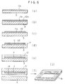
- As shown in Fig. 5, an
optical recording member 7 is constituted by a coloredorganic material layer 11 and a transparent figure image formingmaterial layer 112 to build a layered structure. The coloredorganic material layer 11 is formed on the high surface flatnesscard front board 3 to have a thickness in the range of 300 angstroms to 10 microns. For instance, a solution which is prepared by dissolving NK2014 or NK125 (both of them being produced by Nippon Kanko-Shikiso Kenkyusho Co., Ltd.), IR-820 (produced by Nippon Kayaku Co., Ltd.) or the like in a mixture of cyclohexanone and dichloromethane having a mixing ratio of 1 : 1 by 1 % by weight is employable as material constituting the coloredorganic material layer 11. - The transparent figure image forming
material layer 112 is formed on the coloredorganic material layer 11 to have a thickness in the range of 0.1 to 50 microns. For instance, G-90 (produced by Tokyo Ohka kogyo Co., Ltd.), gelatin, PVA or the like are employable as transparent figure image building material. Incidentally, a plurality ofoptical recording members 7 may be formed one above another. - Next, description will be made below with reference to Fig. 6 as to a method of producing the optical recording card as constructed in the above-described manner.
- First, a colored organic material 11a is coated on the high surface flatness
card front board 3 by a process of spin-coating or the like. As colored organic material 11a, a solution which is prepared by dissolving NK2014 or NK125 (both of them being produced by Nippon Kanko-Shikiso Kenkyusho Co., Ltd.), IR-820(produced by Nippon Kayaku Co., Ltd.) or the like in a mixture of cyclohexanone and dichloromethane having a mixing ratio of 1 : 1 by 1 % by weight is used by a process of coating. After completion of the coating, it is subjected to drying. After it is dried, it has a thickness of about 500 angstroms (see Fig. 6(a)). - Next, a transparent figure
image building material 112a is coated on the colored organic material 11a by a process of spin-coating (see Fig. 6(b)). As transparent figureimage building material 112a, a mixture comprising 10 parts of G-90 (produced by Tokyo Ohka kogyo Co., Ltd.) and 1 part of 1.0 % ammonium dichromate is employable. After completion of the coating, it is subjected to drying. After it is dried, it has a thickness of about 0.4 micron. - Next, the transparent figure
image building material 112a is removed by patterning with the exception of a part corresponding to theoptical recording member 7 forming region 6. This causes a transparent figure image formingmaterial layer 112 to be formed (see Fig. 6(c)). - Next, a colored
organic material layer 11 is formed by dissolving the colored organic material 11a by using the transparent figure image formingmaterial layer 112 as a mask. - An
optical recording member 7 is completed by way of the steps as described above (see Fig. 6(d)). - Next, an
adhesive layer 13 is coated from the above of the optical recording member 7 (see Fig. 6(e)) and the cardrear board 4 is adhesively secured to theoptical recording member 7 with theadhesive layer 13 interposed therebetween (see Fig. 6(f)). - Finally, the completed layered structure is punched to assume a predetermined shape as a card whereby the optical recording card 1 is completed (see Fig. 6(g)).
- When optical informations are written onto the
optical recording card 11 as constructed in the above-described manner, as shown in Fig. 7, a laser beam is emitted onto the coloredorganic material layer 11 from the above of thecard front board 3 of the optical recording card 1. This causes a part of the coloredorganic material layer 11 onto which the laser beam has been emitted to be deformed. At the same time, this deformation is absorbed by dissolution of the transparent figure image formingmaterial layer 112 whereby apit 10 is formed by concavities and convexities which are representative of the surface state of the coloredorganic material layer 11. Reading of thepit 10 is achieved by presence or absence of reflected light from the concavities and convexities representative of the surface state of the coloredorganic material layer 11 or a degree of intensity of the reflected light. - As will be apparent from the above description, the optical recording card of the invention is inexpensive, and the colored organic material layer and the transparent figure image forming material layer can be formed by employing a well-established method in relation to a conventional thin film forming technique. Thus, the optical recording member can be easily produced and therefore the optical recording card of the invention itself can be easily produced at an inexpensive cost.
- Further, since the optical recording member is adhesively enveloped between the card front board and the card rear board with the use of an adhesive, it has stability for a long period of time.
- Moreover, since the the optical recording member is formed directly on the high surface flatness card front board, the recording surface of the optical recording member is excellent in surface flatness and an intensity of adhesion of the optical recording member to the card front board is excellent too.
- While the present invention has been described above with respect to a few preferred embodiments thereof. it should of course be understood that it should not be limited only to them but various changes or modifications may be made in a suitable manner without any departure from the spirit and scope of the invention as defined by the appended claims.
Claims (10)
- An optical recording card (1) having a writable optical recording member (7) is held between a card front board (3) and a card rear board (4) which are adhered to one another, characterised in that the optical recording member (7) includes a coloured organic material layer (11) and an aluminum deposited layer (12) in the form of a layered structure, and the optical recording member (7) is held between said card front board (3) and said card rear board (4) in such a manner that said coloured organic material layer (11) is located on the light emitting side.
- The optical recording card (1) of claim 1 wherein said card front board (3) is constituted by material having an excellent light permeability such as glass or transparent resin such as acrylic resin, epoxy resin, polyester resin, polyvinyl chloride resin, polysulfon resin, polyethersulfon resin or polycarbonate resin.
- The optical recording card (1) of claim 1 or claim 2 wherein said card rear board (4) comprises a plate made of glass or synthetic resin such as acrylic resin, epoxy resin, polyester resin, polyvinyl chloride resin, polysulfon resin, polyethersulfon resin or polycarbonate resin.
- The optical recording card (1) of any preceding claim wherein said coloured organic material layer has a thickness in the range of 300 angstroms to 10 microns.
- The optical recording card (1) of any preceding claim wherein said aluminum deposited layer (12) has a thickness less than about 1000 angstroms.
- A method of producing an optical recording card (1) of the type including a writable optical recording member (7) which is adhesively held between a card front board (3) and a card rear board (4) with the use of an adhesive, characterised in that said method comprises the steps of;
forming a coloured organic material layer (11) in an optical recording member forming region (5) located on one surface of said transparent card front board (3);
next, forming an aluminum deposited layer (12) on said coloured organic material layer (11), and then,
adhesively securing said card rear board (4) to said card front board (3) with the use of an adhesive in such a manner as to cover said coloured organic material layer (11) and said aluminum deposited layer (12). - The method of claim 6 wherein said card front board (3) is constituted by material having an excellent light permeability such as glass or transparent resin such as acrylic resin, epoxy resin, polyester resin, polyvinyl chloride resin, polysulfon resin, polyethersulfon resin or polycarbonate resin.
- The method of claim 6 or claim 7 wherein said card rear board (4) comprises a plate made of glass or synthetic resin such as acrylic resin, epoxy resin, polyester resin, polyvinyl chloride resin, polysulfon resin, polyethersulfon resin or polycarbonate resin.
- The method or one of claim 6 to 8 wherein said coloured organic material layer (11) is coated by a process of spin coating, roll coating or the like and a dried thin film thereof has a thickness in the range of 300 angstrom to 10 microns.
- The method of one of claims 6 to 9 wherein said aluminum deposited layer (12) is formed by vacuum depositing and a deposited thin film thereof has a thickness less than 1000 angstroms.
Applications Claiming Priority (5)
| Application Number | Priority Date | Filing Date | Title |
|---|---|---|---|
| JP304627/86 | 1986-12-20 | ||
| JP61304626A JPS63157336A (en) | 1986-12-20 | 1986-12-20 | Optical record card and its production |
| JP304626/86 | 1986-12-20 | ||
| JP61304627A JPS63157337A (en) | 1986-12-20 | 1986-12-20 | Optical recording card and its production |
| EP87311075A EP0272875B1 (en) | 1986-12-20 | 1987-12-16 | Optical recording card and method of producing the same |
Related Parent Applications (1)
| Application Number | Title | Priority Date | Filing Date |
|---|---|---|---|
| EP87311075.3 Division | 1987-12-16 |
Publications (3)
| Publication Number | Publication Date |
|---|---|
| EP0486482A2 true EP0486482A2 (en) | 1992-05-20 |
| EP0486482A3 EP0486482A3 (en) | 1992-07-08 |
| EP0486482B1 EP0486482B1 (en) | 1995-02-15 |
Family
ID=26563976
Family Applications (2)
| Application Number | Title | Priority Date | Filing Date |
|---|---|---|---|
| EP92200453A Expired - Lifetime EP0486482B1 (en) | 1986-12-20 | 1987-12-16 | Optical recording card and method of producing the same |
| EP87311075A Expired - Lifetime EP0272875B1 (en) | 1986-12-20 | 1987-12-16 | Optical recording card and method of producing the same |
Family Applications After (1)
| Application Number | Title | Priority Date | Filing Date |
|---|---|---|---|
| EP87311075A Expired - Lifetime EP0272875B1 (en) | 1986-12-20 | 1987-12-16 | Optical recording card and method of producing the same |
Country Status (4)
| Country | Link |
|---|---|
| EP (2) | EP0486482B1 (en) |
| AT (1) | ATE118635T1 (en) |
| CA (1) | CA1324669C (en) |
| DE (2) | DE3782812T2 (en) |
Cited By (3)
| Publication number | Priority date | Publication date | Assignee | Title |
|---|---|---|---|---|
| US5555544A (en) * | 1992-01-31 | 1996-09-10 | Massachusetts Institute Of Technology | Tapered semiconductor laser oscillator |
| DE19721527C1 (en) * | 1997-05-22 | 1998-11-05 | Still Gmbh | Unit consisting of an internal combustion engine, generator and pump unit |
| SG92678A1 (en) * | 1999-03-16 | 2002-11-19 | Maurer Electronics Gmbh | Method for recording image information |
Families Citing this family (7)
| Publication number | Priority date | Publication date | Assignee | Title |
|---|---|---|---|---|
| US5017414A (en) * | 1989-01-17 | 1991-05-21 | Del Mar Avionics | Method for manufacturing a second surface optical storage device |
| JP2802520B2 (en) * | 1989-10-20 | 1998-09-24 | 共同印刷株式会社 | Sealed optical card |
| CA2068618A1 (en) * | 1991-05-21 | 1992-11-22 | Tadahiko Mizukuki | Optical recording medium and production thereof |
| EP0972632B1 (en) * | 1998-07-15 | 2004-08-04 | Agfa-Gevaert | A data card comprising a laser recording medium and a thin glass layer |
| EP1048628A1 (en) * | 1999-04-30 | 2000-11-02 | Schott Glas | Polymer coated glassfoil substrate |
| ATE248782T1 (en) * | 1999-01-11 | 2003-09-15 | Schott Displayglas Gmbh | POLYMER COATED THIN GLASS FILM SUBSTRATES |
| DE102012215742A1 (en) * | 2012-09-05 | 2014-03-06 | Bundesdruckerei Gmbh | Safety and / or value product |
Citations (4)
| Publication number | Priority date | Publication date | Assignee | Title |
|---|---|---|---|---|
| DE2826122A1 (en) * | 1977-06-14 | 1978-12-21 | Fuji Photo Film Co Ltd | RECORDING MATERIAL |
| JPS5862096A (en) * | 1981-10-09 | 1983-04-13 | Matsushita Electric Ind Co Ltd | Optical information recording medium |
| JPS5933191A (en) * | 1982-08-18 | 1984-02-22 | Konishiroku Photo Ind Co Ltd | Optical information recording medium |
| EP0158906A2 (en) * | 1984-03-31 | 1985-10-23 | Dai Nippon Insatsu Kabushiki Kaisha | Optical card |
-
1987
- 1987-12-16 DE DE8787311075T patent/DE3782812T2/en not_active Expired - Fee Related
- 1987-12-16 AT AT92200453T patent/ATE118635T1/en not_active IP Right Cessation
- 1987-12-16 DE DE3751073T patent/DE3751073T2/en not_active Expired - Fee Related
- 1987-12-16 EP EP92200453A patent/EP0486482B1/en not_active Expired - Lifetime
- 1987-12-16 EP EP87311075A patent/EP0272875B1/en not_active Expired - Lifetime
- 1987-12-21 CA CA000554935A patent/CA1324669C/en not_active Expired - Fee Related
Patent Citations (4)
| Publication number | Priority date | Publication date | Assignee | Title |
|---|---|---|---|---|
| DE2826122A1 (en) * | 1977-06-14 | 1978-12-21 | Fuji Photo Film Co Ltd | RECORDING MATERIAL |
| JPS5862096A (en) * | 1981-10-09 | 1983-04-13 | Matsushita Electric Ind Co Ltd | Optical information recording medium |
| JPS5933191A (en) * | 1982-08-18 | 1984-02-22 | Konishiroku Photo Ind Co Ltd | Optical information recording medium |
| EP0158906A2 (en) * | 1984-03-31 | 1985-10-23 | Dai Nippon Insatsu Kabushiki Kaisha | Optical card |
Non-Patent Citations (2)
| Title |
|---|
| PATENT ABSTRACTS OF JAPAN vol. 7, no. 153 (M-226)(1298) 5 July 1983 & JP-A-58 062 096 ( MATSUSHITA DENKI SANGYO K.K. ) 13 April 1983 * |
| PATENT ABSTRACTS OF JAPAN vol. 8, no. 132 (M-303)(1569) 20 June 1984 & JP-A-59 033 191 ( KONISHIROKU SHASHIN KOGYO K.K. ) 22 February 1984 * |
Cited By (4)
| Publication number | Priority date | Publication date | Assignee | Title |
|---|---|---|---|---|
| US5555544A (en) * | 1992-01-31 | 1996-09-10 | Massachusetts Institute Of Technology | Tapered semiconductor laser oscillator |
| DE19721527C1 (en) * | 1997-05-22 | 1998-11-05 | Still Gmbh | Unit consisting of an internal combustion engine, generator and pump unit |
| SG92678A1 (en) * | 1999-03-16 | 2002-11-19 | Maurer Electronics Gmbh | Method for recording image information |
| US6633321B1 (en) | 1999-03-16 | 2003-10-14 | Maurer Electronics Gmbh | Method for recording image information |
Also Published As
| Publication number | Publication date |
|---|---|
| DE3751073D1 (en) | 1995-03-23 |
| EP0272875B1 (en) | 1992-11-25 |
| DE3751073T2 (en) | 1995-09-14 |
| DE3782812T2 (en) | 1993-04-22 |
| EP0486482A3 (en) | 1992-07-08 |
| EP0272875A3 (en) | 1990-01-17 |
| EP0272875A2 (en) | 1988-06-29 |
| CA1324669C (en) | 1993-11-23 |
| EP0486482B1 (en) | 1995-02-15 |
| DE3782812D1 (en) | 1993-01-07 |
| ATE118635T1 (en) | 1995-03-15 |
Similar Documents
| Publication | Publication Date | Title |
|---|---|---|
| US4945215A (en) | Optical recording card having hologram contained therein and method of producing the same | |
| US5010243A (en) | Method of producing an optical recording card having a hologram contained therein | |
| EP0485366B1 (en) | Process for preparing optical data cards | |
| US5217844A (en) | Optical recording medium, method of producing the same and method of producing the optical recording card | |
| EP0272875B1 (en) | Optical recording card and method of producing the same | |
| JP2958964B2 (en) | Retroreflective adhesive sheet | |
| EP0239188B1 (en) | Preformatted optical recording medium and method of producing the same | |
| US4956215A (en) | Optical recording card and method of producing the same | |
| US6177176B1 (en) | Information recording medium readable from a side edge | |
| US5114531A (en) | Method of producing masks for rom type optical recording cards and method of inspecting masks | |
| JPS62259244A (en) | Optical reading card | |
| JP2871148B2 (en) | card | |
| JP3516184B2 (en) | Optical disk and method of manufacturing optical disk | |
| JPH0480458B2 (en) | ||
| JPS62291731A (en) | Optical information recording body | |
| JPH02177140A (en) | Optical card | |
| JPH027247A (en) | Manufacture of optical card | |
| JPS637532A (en) | Optical card | |
| JP2628574B2 (en) | Thermal magnetic recording method | |
| JPS637535A (en) | Optical card | |
| JPH04155632A (en) | Thermal recording medium | |
| JPH07112592A (en) | Magnetic display medium | |
| JPH0646461B2 (en) | Optical card manufacturing method | |
| JPH10222951A (en) | Cassette | |
| JPS63239629A (en) | Optical recording card and reader for optical recording card |
Legal Events
| Date | Code | Title | Description |
|---|---|---|---|
| PUAI | Public reference made under article 153(3) epc to a published international application that has entered the european phase |
Free format text: ORIGINAL CODE: 0009012 |
|
| PUAL | Search report despatched |
Free format text: ORIGINAL CODE: 0009013 |
|
| 17P | Request for examination filed |
Effective date: 19920305 |
|
| AC | Divisional application: reference to earlier application |
Ref document number: 272875 Country of ref document: EP |
|
| AK | Designated contracting states |
Kind code of ref document: A2 Designated state(s): AT BE CH DE FR GB IT LI NL SE |
|
| AK | Designated contracting states |
Kind code of ref document: A3 Designated state(s): AT BE CH DE FR GB IT LI NL SE |
|
| 17Q | First examination report despatched |
Effective date: 19931103 |
|
| GRAA | (expected) grant |
Free format text: ORIGINAL CODE: 0009210 |
|
| AC | Divisional application: reference to earlier application |
Ref document number: 272875 Country of ref document: EP |
|
| AK | Designated contracting states |
Kind code of ref document: B1 Designated state(s): AT BE CH DE FR GB IT LI NL SE |
|
| PG25 | Lapsed in a contracting state [announced via postgrant information from national office to epo] |
Ref country code: LI Effective date: 19950215 Ref country code: CH Effective date: 19950215 Ref country code: BE Effective date: 19950215 Ref country code: AT Effective date: 19950215 |
|
| REF | Corresponds to: |
Ref document number: 118635 Country of ref document: AT Date of ref document: 19950315 Kind code of ref document: T |
|
| REF | Corresponds to: |
Ref document number: 3751073 Country of ref document: DE Date of ref document: 19950323 |
|
| ET | Fr: translation filed | ||
| ITF | It: translation for a ep patent filed |
Owner name: SOCIETA' ITALIANA BREVETTI S.P.A. |
|
| PG25 | Lapsed in a contracting state [announced via postgrant information from national office to epo] |
Ref country code: SE Effective date: 19950515 |
|
| REG | Reference to a national code |
Ref country code: CH Ref legal event code: PL |
|
| PLBE | No opposition filed within time limit |
Free format text: ORIGINAL CODE: 0009261 |
|
| STAA | Information on the status of an ep patent application or granted ep patent |
Free format text: STATUS: NO OPPOSITION FILED WITHIN TIME LIMIT |
|
| 26N | No opposition filed | ||
| PGFP | Annual fee paid to national office [announced via postgrant information from national office to epo] |
Ref country code: GB Payment date: 19990114 Year of fee payment: 12 |
|
| PGFP | Annual fee paid to national office [announced via postgrant information from national office to epo] |
Ref country code: DE Payment date: 19990125 Year of fee payment: 12 |
|
| PGFP | Annual fee paid to national office [announced via postgrant information from national office to epo] |
Ref country code: FR Payment date: 19990126 Year of fee payment: 12 |
|
| PGFP | Annual fee paid to national office [announced via postgrant information from national office to epo] |
Ref country code: NL Payment date: 19990131 Year of fee payment: 12 |
|
| PG25 | Lapsed in a contracting state [announced via postgrant information from national office to epo] |
Ref country code: GB Free format text: LAPSE BECAUSE OF NON-PAYMENT OF DUE FEES Effective date: 19991216 |
|
| PG25 | Lapsed in a contracting state [announced via postgrant information from national office to epo] |
Ref country code: NL Free format text: LAPSE BECAUSE OF NON-PAYMENT OF DUE FEES Effective date: 20000701 |
|
| GBPC | Gb: european patent ceased through non-payment of renewal fee |
Effective date: 19991216 |
|
| PG25 | Lapsed in a contracting state [announced via postgrant information from national office to epo] |
Ref country code: FR Free format text: LAPSE BECAUSE OF NON-PAYMENT OF DUE FEES Effective date: 20000831 |
|
| NLV4 | Nl: lapsed or anulled due to non-payment of the annual fee |
Effective date: 20000701 |
|
| PG25 | Lapsed in a contracting state [announced via postgrant information from national office to epo] |
Ref country code: DE Free format text: LAPSE BECAUSE OF NON-PAYMENT OF DUE FEES Effective date: 20001003 |
|
| REG | Reference to a national code |
Ref country code: FR Ref legal event code: ST |
|
| PG25 | Lapsed in a contracting state [announced via postgrant information from national office to epo] |
Ref country code: IT Free format text: LAPSE BECAUSE OF NON-PAYMENT OF DUE FEES;WARNING: LAPSES OF ITALIAN PATENTS WITH EFFECTIVE DATE BEFORE 2007 MAY HAVE OCCURRED AT ANY TIME BEFORE 2007. THE CORRECT EFFECTIVE DATE MAY BE DIFFERENT FROM THE ONE RECORDED. Effective date: 20051216 |