EP0486331A2 - Digital distribution apparatus - Google Patents
Digital distribution apparatus Download PDFInfo
- Publication number
- EP0486331A2 EP0486331A2 EP91402605A EP91402605A EP0486331A2 EP 0486331 A2 EP0486331 A2 EP 0486331A2 EP 91402605 A EP91402605 A EP 91402605A EP 91402605 A EP91402605 A EP 91402605A EP 0486331 A2 EP0486331 A2 EP 0486331A2
- Authority
- EP
- European Patent Office
- Prior art keywords
- contacts
- module
- frame
- normally closed
- plug
- Prior art date
- Legal status (The legal status is an assumption and is not a legal conclusion. Google has not performed a legal analysis and makes no representation as to the accuracy of the status listed.)
- Granted
Links
- 238000003780 insertion Methods 0.000 abstract description 11
- 230000037431 insertion Effects 0.000 abstract description 11
- 238000012360 testing method Methods 0.000 description 8
- 238000012544 monitoring process Methods 0.000 description 6
- 238000010618 wire wrap Methods 0.000 description 5
- 238000000034 method Methods 0.000 description 4
- 230000000717 retained effect Effects 0.000 description 4
- 239000004020 conductor Substances 0.000 description 3
- 230000002441 reversible effect Effects 0.000 description 3
- 238000012986 modification Methods 0.000 description 2
- 230000004048 modification Effects 0.000 description 2
- 230000000712 assembly Effects 0.000 description 1
- 238000000429 assembly Methods 0.000 description 1
- 238000006243 chemical reaction Methods 0.000 description 1
- 230000001419 dependent effect Effects 0.000 description 1
- 238000013461 design Methods 0.000 description 1
- 239000002184 metal Substances 0.000 description 1
- 239000000700 radioactive tracer Substances 0.000 description 1
Images


Classifications
-
- H—ELECTRICITY
- H04—ELECTRIC COMMUNICATION TECHNIQUE
- H04Q—SELECTING
- H04Q1/00—Details of selecting apparatus or arrangements
- H04Q1/02—Constructional details
- H04Q1/14—Distribution frames
-
- H—ELECTRICITY
- H04—ELECTRIC COMMUNICATION TECHNIQUE
- H04Q—SELECTING
- H04Q11/00—Selecting arrangements for multiplex systems
- H04Q11/04—Selecting arrangements for multiplex systems for time-division multiplexing
Definitions
- This invention pertains to the telecommunications industry. More particularly, this invention pertains to a digital distribution apparatus for use in a telecommunications network.
- the telecommunications industry requires cross- connecting and switching functions for a variety of equipment.
- the industry has utilized manually operated digital system cross-connect (DSX) apparatus for connecting two or more units of telecommunications equipment.
- DSX digital system cross-connect
- the DSX equipment could provide cross-connect, monitoring, and other access functions to the telecommunication network.
- an apparatus for providing access to a plurality of telecommunication lines.
- the apparatus includes a frame which carries a plurality of normally closed contacts.
- the telecommunication lines are terminated on the normally closed contacts.
- a plurality of modules are provided to be releasably attached to the frame with electrical circuit elements on the modules engaging the normally closed contacts to open the contacts and create a new signal path through the module upon insertion of the module into the frame.
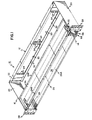
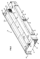
- the apparatus 10 is shown as including a frame 12 and a plurality of modules or jack cards 14 (only one of which is shown in Figs. 1 and 3).
- the frame 12 includes a chassis 16 and a plurality of connector assemblies 18 (only two of which are shown in Fig. 2 and only one of which is shown in Fig. 3).
- Chassis 16 is preferably formed of sheet metal and includes spaced apart side walls 20 connected by a rear wall 22, a forward top panel 24 and a forward bottom panel 26. Side flanges 28 are connected to side walls 20 to permit the chassis 16 to be mounted in stacked vertical array with a plurality of other chassis (not shown) in a mainframe or bay (not shown).
- Rear wall 22 is provided with openings 30 therethrough sized to receive termination blocks 32.
- Blocks 32 are provided with wire wrap termination pins 34 extending therethrough. It will be appreciated that termination blocks having termination pins such as blocks 32 and pins 34 are well known in the art and form no part of this invention per se.
- top panel 24 and bottom panel 26 are spaced apart to define a jack card receiving area 36 which extends between sidewalls 20 and from leading edges 24A,26A of panels 24,26, respectively, to be trailing edges 24B,26B.
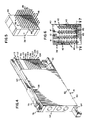
- the connector assembly 18 includes a block dielectric body 38 shown best in Figs. 5 and 6.
- the forward face 40 of the block body 38 is provided with a plurality of vertical slots 41 each having a plurality of vertically aligned contact receiving chambers 42.
- the chambers 42 each receives a pair of spring contacts 44 which cooperate to define a normally closed switch 45 (illustrated best in Fig. 7).
- the spring contacts 44 are provided with wire wrap termination pins 46 which extend through the rear face 48 of block 38 as best shown in Fig. 5.
- the block bodies 38 are disposed in side-by-side relation within the jack card receiving area 36.
- the bodies are sized to have a vertical dimension for the body 18 to extend between top and bottom panels 24,26.
- the bodies 18 are disposed adjacent the trailing edges 24B,26B with the pins 46 extending away from area 36.
- the jack cards 14 include a dielectric body 50 which carries a printed circuit board card 52.
- the jack card 14 extends from a leading edge 54 of body 50 to a trailing edge 56 of card 52.
- An upper edge 58 of body 50 is provided with an axially extending rail 60.
- a lower edge 62 of body 50 is provided with a lower rail 64 (only a portion of which is shown in Fig. 4) similar in structure to that of rail 60.
- the vertical dimension (i.e., the distance between upper edge 58 and lower edge 62) of jack card 14 is selected for the card to be received with in area 36 with upper edge 58 opposing panel 24 and with lower edge 62 opposing panel 26.
- Bottom panel 26 is provided with a plurality of transverse slots 66 sized to slidably receive lower rail 64 (see Figs. 1 and 3).
- the connector assembly 18 includes an upper slotted rail guide 68.
- Guide 68 is provided with clips 70 disposed to align with openings 72 formed in upper panel 24. Accordingly, the rail guide 68 is to be retained against an inner surface of upper panel 24.
- the rail guide 68 is provided with a plurality of transverse slots 74 sized to slidably receive rail 60.
- slots 66, rail guide 68 and back panel 18 are disposed for the elements of each to cooperate for jack card 14 to be slidably received between panels 24,26 and with the trailing edge 56 of card 52 receivable within a vertical slot 41 of body 38.
- Retaining clips 76 are provided on the jack in body 14. The clips 76 have ramps 78 which are releasably received within openings 80 formed in rail guide 68 to releasably secure jack card 14 in an inserted position in jack card receiving area 36 (as shown in Fig. 1).
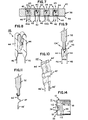
- Forward edge 54 of jack card 15 is provided with a plurality of holes or ports extending therethrough.
- the plurality of ports includes a monitor (or MON) port 82, an OUT port 84 and an IN port 86.
- the jack card carries an electrical circuit 88 which includes a plurality of spring contacts.
- the plurality of spring contacts includes an IN tip normal spring 90 and an IN tip spring 91.
- the plurality also includes an IN ring normal spring 92 and an IN ring spring 93, an OUT tip normal spring 94 and an OUT tip spring 95.
- the plurality also includes an OUT ring normal spring 96 and an OUT ring spring 97, a monitor tip spring 98, a monitor ring spring 99, a first LED spring 100 and a second LED spring 101.
- Springs 91 and 93 are disposed to be engaged by the tip and ring, respectively, of an electrical jack plug (not shown) inserted within the IN port 86.
- Springs 95,97 are selected to be engaged by the tip and ring of a plug, not shown, inserted within the OUT port 84.
- springs 98,99 are disposed to be engaged by the tip and ring of a plug, not shown, inserted within the MON port 82.
- Spring pairs 90-91, 92-93, 94-95, and 96-97 are in normal contact in the absence of a plug within either of ports 84,86 and will be opened by insertion of a plug.
- Springs 98,99 are connected across a resistance to springs 95,97.
- Spring 100 is engaged into electrical contact with spring 101 by means of spring 99 urging spring 100 via a dielectric pusher 102 against spring 101.
- Springs such as springs 90-101 are retained within dielectric body 50 in a manner similar to springs retained in a body such as that shown in commonly assigned U.S. Patent 4,840,568.
- the trailing edge 56 of card 52 is provided with a plurality of electrical contact pads 104-113 which are connected to springs 90-97 and 100-101, respectively, via circuit paths 114-123.
- electrical contact pads 104-113 which are connected to springs 90-97 and 100-101, respectively, via circuit paths 114-123.
- the use of LED springs 100,101 may be optional.
- contacts pads 112,113 could be eliminated.
- the block 38 includes vertical columns of eight spaces 42 to accommodate only pads 104-111).
- the circuit boards 52 may be provided with additional electrical circuitry (such as repeaters or other circuit enhancement circuitry).
- a plurality of spring contacts 44 are retained within the chambers 42 of assembly 18. Paired spring contacts 44 cooperate to define normally closed spring switches 45. Namely, the spring contacts pairs 44 are in electrical engagement on the absence of a card within slots 41.
- the normally closed spring contacts 44 are best illustrated in Figs. 7 and 8 where the contact ends 44a are shown in electrical engagement in the absence of a card 52 within the chambers 42.
- the spring contacts 44 are also so-called make-before-break normally closed spring contacts which make electrical contact with a pad such as pads 104-111 before breaking or opening the electrical connection across the spring contacts 44.
- Fig. 9 shows a card 52 with pads 104", 105" in electrical contact with spring contacts 44 before forcing the spring contacts 44 apart upon full insertion of the card 52.
- Figs. 10 and 11 show an alternative arrangement for a make-before-break normally closed spring contact pairs with spring contacts 44' connected across a shunt bar 47.
- Fig. 11 shows electrical contact being made with the cards 44' before the spring contacts 44' are urged away from the shunt bar 47.
- the contact pads 104-113 are shown on the same side of the card 52 for purposes of clarity of the illustrations.
- the card 52 is used in conjunction with side-by-side paired contacts 44' as shown in Figs. 10 and 11. If opposing paired contacts 44 (as shown in Figs. 7-9) are used the pads 104-113 are disposed on opposite sides of the card 52 (as illustrated by pads 104", 105" in Fig. 9).
- Fig. 12 is shown for use with the jack card 14 of Fig. 4A which includes the MON port 82 with monitor springs 100,101.
- the frame 12 is provided with an LED 114 connected via springs 100,101 to a voltage source 115 and a ground 117. The LED is illuminated upon insertion of a plug in the MON port 82.
- monitor springs can be omitted from the jack card 14 with monitor springs 100',101' canried by the frame 12 (as shown in Fig. 13).
- tip and ring conductors of a telecommunications network may be terminated on the wire wrap termination pins 34 of blocks 32.
- the pins 34 are hard wired to the spring switches 45 which are normally closed.
- a signal flows through the apparatus 10 without modification or access in the absence of a jack card 14.
- the presence of a jack card 14 results in the signal now flowing through the circuitry 88 of the jack card 14.
- Insertion of a plug into ports 82,84,86 permits monitoring and test access to the telecommunications network in a manner similar to that provided by DSX equipment such as that shown in U.S. Patent 4,840,568.
- the reader will note a significant difference between the structure of the present invention in the aforementioned U.S.
- Patent 4,840,568 is that the spring contacts of the connector assembly of the aforementioned patent (items 300 in the aforementioned patent) do not include normally closed pairs of contacts. As a result, the prior DSX apparatus was not suitable for signal through in the absence of spring carrying jack cards.
- the present apparatus is particularly suitable for use in conversion of prior art DSX networks to updated DCS networks.
- DCS Digital Cross-Connect Systems
- EDSX Electronic DSX equipment
- DACS Digital Access Cross-Connect Systems
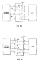
- Fig. 22 shows a DSX equipment bay 120 connected through tip and ring lines 122 to network equipment 124.
- FIG. 23 shows the DSX replaced with an EDSX 126 and an apparatus 10 of the present invention.
- the apparatus 10 in the absence of jack cards 14 provides signal flow through the apparatus 10 between the equipment 124 and the EDSX 126. Insertion of jack cards 14 within the apparatus 10 permits manual test access and monitoring as well as optional circuit enhancement without interference with the EDSX 126. The manual access capability is particularly desirable in the event of disfunction of EDSX equipment 126.
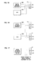
- Fig. 15 illustrates use of the apparatus 10 for test access where the spring contacts 44 are shown normally closed and jack cards 14 are not inserted within the frame.
- the apparatus 10 provides a simple flow-through of a signal between network equipment 200 and a DCS 202. At the option of a user, the signal may be accessed by insertion of a jack card 14 into apparatus 10.
- Fig. 16 shows use of the apparatus 10 in an interconnect function.
- Fig. 17 shows use of the apparatus in a cross-connect function.
- An alternative structure of the present invention is to provide for a jack card 14 which may be flipped in its orientation to reverse the test access capabilities of the jack card. Such an embodiment is shown in Figs. 18 and 19.
- a reversible jack card 214 is shown inserted within connector assembly 218 which is carried by chassis 216.
- the IN and OUT conductor pads i.e. pads 104'-111' connected to springs 90'-97'
- the card 214 may be reversed about axis X-X and reinserted. With this embodiment, the card 214 may be inserted in its first or upright position as shown in Fig. 18.
- the jack card Upon insertion of a plug into the IN, OUT or monitor ports of jack card 214, the jack card will function similar to that of the embodiment of Fig. 4A.
- the present embodiment permits the jack card 214 to be rotated about axis X-X and be inserted in the inverted position as in Fig. 19.
- This permits alternative test access (indicated by the designations in Figs. 18 and 19 of "NE OUT” and "NE IN” for network equipment IN and OUT and “DCS IN” and “DCS OUT” for Digital Cross-Connect System IN and OUT).
- the monitor port is now connected to alternatively the OUT or the IN equipment lines depending upon the orientation of the card 214.
- the LED spring contacts are not in electrical contact upon flipping of the jack card assembly.
- an alternative embodiment to that design would be an inclusion of ground and tracer light leads disposed to electrically engage the pads when the jack card is in the flip position of Fig. 19.
- Figs. 20 and 21 show use of the apparatus of Figs. 18 and 19 in a network indicating alternate directions for test access and monitoring dependent upon flipping of the jack card assembly 214.
Landscapes
- Computer Networks & Wireless Communication (AREA)
- Engineering & Computer Science (AREA)
- Structure Of Telephone Exchanges (AREA)
- Analysing Materials By The Use Of Radiation (AREA)
- Processing Of Color Television Signals (AREA)
- Mobile Radio Communication Systems (AREA)
- Auxiliary Devices For Music (AREA)
- Arrangements For Transmission Of Measured Signals (AREA)
- Noodles (AREA)
- Coupling Device And Connection With Printed Circuit (AREA)
- Cable Transmission Systems, Equalization Of Radio And Reduction Of Echo (AREA)
- Distribution Board (AREA)
- Details Of Connecting Devices For Male And Female Coupling (AREA)
Abstract
Description
- This invention pertains to the telecommunications industry. More particularly, this invention pertains to a digital distribution apparatus for use in a telecommunications network.
- The telecommunications industry requires cross- connecting and switching functions for a variety of equipment. Historically, the industry has utilized manually operated digital system cross-connect (DSX) apparatus for connecting two or more units of telecommunications equipment. The DSX equipment could provide cross-connect, monitoring, and other access functions to the telecommunication network.
- In recent years, the telecommunications industry has considered the implementation of electronic digital signal cross-connect (EDSX) equipment to replace conventional manual DSX equipment. An example of a method for replacing DSX equipment with EDSX is shown in commonly assigned U.S. Patent No. 4,941,165 entitled "Hot Cut Procedure For Telecommunication Network".
- When utilizing EDSX equipment, it is desirable to retain opportunities for manual cross-connect as well as test access and monitoring functions independent of the EDSX equipment. It is an object of the present invention to provide such an apparatus. Also, it is an object of the present invention to provide line access equipment which may be used independent of an EDSX apparatus.
- According to a preferred embodiment of the present invention an apparatus is disclosed for providing access to a plurality of telecommunication lines. The apparatus includes a frame which carries a plurality of normally closed contacts. The telecommunication lines are terminated on the normally closed contacts. A plurality of modules are provided to be releasably attached to the frame with electrical circuit elements on the modules engaging the normally closed contacts to open the contacts and create a new signal path through the module upon insertion of the module into the frame.
-
- Fig. 1 is a front, top and right side perspective view of an apparatus according to the present invention;
- Fig. 2 is a rear, top and right side perspective view of the apparatus of Fig. 1;
- Fig. 3 is an exploded perspective view of the apparatus of Fig. 1;
- Fig. 4 is a perspective view of a jack card for use in the apparatus of Fig. 1;
- Fig. 4A is a schematic view of a jack card showing electrical circuit elements carried by the jack card;
- Fig. 5 is a rear, top and right side perspective view of a connector assembly for use in the apparatus of Fig. 1;
- Fig. 6 is a front elevation view of the connector assembly of Fig. 5;
- Fig. 7 is a view taken along line 7-7 in Fig. 6;
- Fig. 8 is a perspective view of a normally closed pair of spring contacts for use in the present invention;
- Fig. 9 is a view showing the spring contacts of Fig. 8 in a position about to be opened by insertion of a card;
- Fig. 10 is a perspective view of an alternative pair of spring contacts for use with the present invention;
- Fig. 11 is a view of the spring contacts of Fig. 10 about to be opened by insertion of a card;
- Fig. 12 is a schematic cross-sectional view of a frame for use with the present invention;
- Fig. 13 is an alternative embodiment of the frame of Fig. 12;
- Fig. 14 is a view showing in cross-section the frame of Fig. 12;
- Fig. 15 is a schematic representation of a first use of the apparatus of the present invention in a telecommunications network;
- Fig. 16 is a schematic representation of a second use of the apparatus of the present invention in a telecommunications network;
- Fig. 17 is a schematic representation of a third use of the apparatus of the present invention in a telecommunications network;
- Fig. 18 is a schematic representation, taken in cross-section, of the apparatus of the present invention with an embodiment of a reversible jack card shown in a first position;
- Fig. 19 is the view of Fig. 18 with the jack card shown in a flipped position;
- Fig. 20 is a schematic representation of the apparatus of Fig. 18 in a telecommunications network;
- Fig. 21 is a schematic representation of the apparatus of Fig. 19 in a telecommunications network;
- Fig. 22 shows, in schematic format, a telecommunications network with a manual DSX in places; and
- Fig. 23 shows, in schematic format, a telecommunications network with an EDSX in use in conjunction with an apparatus of the present invention.
- Referring now to the several drawing figures in which identical elements are numbered identically throughout, a description of the preferred embodiment of the present invention will now be provided.
- With initial reference to Figs. 1-3, the
apparatus 10 is shown as including aframe 12 and a plurality of modules or jack cards 14 (only one of which is shown in Figs. 1 and 3). As will be more fully described, theframe 12 includes achassis 16 and a plurality of connector assemblies 18 (only two of which are shown in Fig. 2 and only one of which is shown in Fig. 3).Chassis 16 is preferably formed of sheet metal and includes spaced apartside walls 20 connected by arear wall 22, aforward top panel 24 and aforward bottom panel 26.Side flanges 28 are connected toside walls 20 to permit thechassis 16 to be mounted in stacked vertical array with a plurality of other chassis (not shown) in a mainframe or bay (not shown). -
Rear wall 22 is provided withopenings 30 therethrough sized to receivetermination blocks 32.Blocks 32 are provided with wirewrap termination pins 34 extending therethrough. It will be appreciated that termination blocks having termination pins such asblocks 32 andpins 34 are well known in the art and form no part of this invention per se. - As shown in Figs. 1-3,
top panel 24 andbottom panel 26 are spaced apart to define a jackcard receiving area 36 which extends betweensidewalls 20 and from leadingedges panels edges - The
connector assembly 18 includes a blockdielectric body 38 shown best in Figs. 5 and 6. Theforward face 40 of theblock body 38 is provided with a plurality ofvertical slots 41 each having a plurality of vertically alignedcontact receiving chambers 42. Thechambers 42 each receives a pair ofspring contacts 44 which cooperate to define a normally closed switch 45 (illustrated best in Fig. 7). - The
spring contacts 44 are provided with wirewrap termination pins 46 which extend through therear face 48 ofblock 38 as best shown in Fig. 5. - As shown in Fig. 2, the
block bodies 38 are disposed in side-by-side relation within the jackcard receiving area 36. The bodies are sized to have a vertical dimension for thebody 18 to extend between top andbottom panels bodies 18 are disposed adjacent thetrailing edges pins 46 extending away fromarea 36. - Referring now to Figs. 4 and 4A, the
jack cards 14 include adielectric body 50 which carries a printedcircuit board card 52. Thejack card 14 extends from a leadingedge 54 ofbody 50 to a trailingedge 56 ofcard 52. Anupper edge 58 ofbody 50 is provided with anaxially extending rail 60. Alower edge 62 ofbody 50 is provided with a lower rail 64 (only a portion of which is shown in Fig. 4) similar in structure to that ofrail 60. - The vertical dimension (i.e., the distance between
upper edge 58 and lower edge 62) ofjack card 14 is selected for the card to be received with inarea 36 withupper edge 58 opposingpanel 24 and withlower edge 62 opposingpanel 26.Bottom panel 26 is provided with a plurality oftransverse slots 66 sized to slidably receive lower rail 64 (see Figs. 1 and 3). Theconnector assembly 18 includes an upper slottedrail guide 68.Guide 68 is provided withclips 70 disposed to align with openings 72 formed inupper panel 24. Accordingly, therail guide 68 is to be retained against an inner surface ofupper panel 24. Therail guide 68 is provided with a plurality of transverse slots 74 sized to slidably receiverail 60. - As shown in Figs. 1-3,
slots 66,rail guide 68 and backpanel 18 are disposed for the elements of each to cooperate forjack card 14 to be slidably received betweenpanels edge 56 ofcard 52 receivable within avertical slot 41 ofbody 38. Retaining clips 76 are provided on the jack inbody 14. Theclips 76 haveramps 78 which are releasably received withinopenings 80 formed inrail guide 68 to releasablysecure jack card 14 in an inserted position in jack card receiving area 36 (as shown in Fig. 1). - Forward edge 54 of jack card 15 is provided with a plurality of holes or ports extending therethrough. The plurality of ports includes a monitor (or MON)
port 82, anOUT port 84 and anIN port 86. As shown in Fig. 4A, the jack card carries anelectrical circuit 88 which includes a plurality of spring contacts. - The plurality of spring contacts includes an IN tip
normal spring 90 and anIN tip spring 91. The plurality also includes an IN ringnormal spring 92 and anIN ring spring 93, an OUT tipnormal spring 94 and anOUT tip spring 95. The plurality also includes an OUT ringnormal spring 96 and anOUT ring spring 97, amonitor tip spring 98, amonitor ring spring 99, afirst LED spring 100 and asecond LED spring 101. -
Springs IN port 86.Springs OUT port 84. Similarly springs 98,99 are disposed to be engaged by the tip and ring of a plug, not shown, inserted within theMON port 82. Spring pairs 90-91, 92-93, 94-95, and 96-97 are in normal contact in the absence of a plug within either ofports Springs springs Spring 100 is engaged into electrical contact withspring 101 by means ofspring 99 urgingspring 100 via adielectric pusher 102 againstspring 101. Springs such as springs 90-101 are retained withindielectric body 50 in a manner similar to springs retained in a body such as that shown in commonly assigned U.S. Patent 4,840,568. - The trailing
edge 56 ofcard 52 is provided with a plurality of electrical contact pads 104-113 which are connected to springs 90-97 and 100-101, respectively, via circuit paths 114-123. As will become apparent, the use of LED springs 100,101 may be optional. In this event, contacts pads 112,113 could be eliminated. (To illustrate this option, theblock 38 includes vertical columns of eightspaces 42 to accommodate only pads 104-111). In addition to permitting test access and monitoring (as will be described), thecircuit boards 52 may be provided with additional electrical circuitry (such as repeaters or other circuit enhancement circuitry). - As previously mentioned, a plurality of
spring contacts 44 are retained within thechambers 42 ofassembly 18. Pairedspring contacts 44 cooperate to define normally closed spring switches 45. Namely, the spring contacts pairs 44 are in electrical engagement on the absence of a card withinslots 41. - The normally
closed spring contacts 44 are best illustrated in Figs. 7 and 8 where the contact ends 44a are shown in electrical engagement in the absence of acard 52 within thechambers 42. Preferably, thespring contacts 44 are also so-called make-before-break normally closed spring contacts which make electrical contact with a pad such as pads 104-111 before breaking or opening the electrical connection across thespring contacts 44. Fig. 9 shows acard 52 withpads 104", 105" in electrical contact withspring contacts 44 before forcing thespring contacts 44 apart upon full insertion of thecard 52. - Figs. 10 and 11 show an alternative arrangement for a make-before-break normally closed spring contact pairs with
spring contacts 44' connected across ashunt bar 47. Fig. 11 shows electrical contact being made with thecards 44' before thespring contacts 44' are urged away from theshunt bar 47. - In Figs. 4 and 4A, the contact pads 104-113 are shown on the same side of the
card 52 for purposes of clarity of the illustrations. With this arrangement, thecard 52 is used in conjunction with side-by-side pairedcontacts 44' as shown in Figs. 10 and 11. If opposing paired contacts 44 (as shown in Figs. 7-9) are used the pads 104-113 are disposed on opposite sides of the card 52 (as illustrated bypads 104", 105" in Fig. 9). - The wire wrap termination pins 46 of the
connector assembly 18 are hard wired to the wire wrap termination pins 34 of the termination blocks 32 bywire conductors 112 as shown in Fig. 14 (and as schematically shown in Figs. 12 and 13). Figs. 12 and 13 shown in schematic format are alternative embodiments of the invention. Fig. 12 is shown for use with thejack card 14 of Fig. 4A which includes theMON port 82 with monitor springs 100,101. With that embodiment, theframe 12 is provided with anLED 114 connected via springs 100,101 to avoltage source 115 and aground 117. The LED is illuminated upon insertion of a plug in theMON port 82. Alternatively, monitor springs can be omitted from thejack card 14 with monitor springs 100',101' canried by the frame 12 (as shown in Fig. 13). - With the apparatus thus described, tip and ring conductors of a telecommunications network may be terminated on the wire wrap termination pins 34 of
blocks 32. Thepins 34 are hard wired to the spring switches 45 which are normally closed. As a result, a signal flows through theapparatus 10 without modification or access in the absence of ajack card 14. The presence of ajack card 14 results in the signal now flowing through thecircuitry 88 of thejack card 14. Insertion of a plug intoports - The present apparatus is particularly suitable for use in conversion of prior art DSX networks to updated DCS networks. (Those skilled in the art will recognize DCS ("Digital Cross-Connect Systems") to include EDSX as well as DACS ("Digital Access Cross-Connect Systems"). As previously mentioned, commonly assigned U.S. Patent No. 4,941,165, teaches a method for replacing manual DSX equipment with electronic DSX equipment (EDSX). Utilization of a so-called hot cut procedure as described in U.S. Patent No. 4,941,165 permits replacement of the manual DSX with the DCS without service interruption. Fig. 22 shows a
DSX equipment bay 120 connected through tip andring lines 122 tonetwork equipment 124. Fig. 23 shows the DSX replaced with anEDSX 126 and anapparatus 10 of the present invention. With the embodiment shown in Fig. 23, the apparatus 10 (in the absence of jack cards 14) provides signal flow through theapparatus 10 between theequipment 124 and theEDSX 126. Insertion ofjack cards 14 within theapparatus 10 permits manual test access and monitoring as well as optional circuit enhancement without interference with theEDSX 126. The manual access capability is particularly desirable in the event of disfunction ofEDSX equipment 126. - Fig. 15 illustrates use of the
apparatus 10 for test access where thespring contacts 44 are shown normally closed andjack cards 14 are not inserted within the frame. In the embodiment of Fig. 15, theapparatus 10 provides a simple flow-through of a signal betweennetwork equipment 200 and aDCS 202. At the option of a user, the signal may be accessed by insertion of ajack card 14 intoapparatus 10. Fig. 16 shows use of theapparatus 10 in an interconnect function. Fig. 17 shows use of the apparatus in a cross-connect function. - An alternative structure of the present invention is to provide for a
jack card 14 which may be flipped in its orientation to reverse the test access capabilities of the jack card. Such an embodiment is shown in Figs. 18 and 19. - In Fig. 18, a
reversible jack card 214 is shown inserted withinconnector assembly 218 which is carried bychassis 216. The IN and OUT conductor pads (i.e. pads 104'-111' connected to springs 90'-97') are shown symmetrically arranged about a rotational axis X-X. Thecard 214 may be reversed about axis X-X and reinserted. With this embodiment, thecard 214 may be inserted in its first or upright position as shown in Fig. 18. Upon insertion of a plug into the IN, OUT or monitor ports ofjack card 214, the jack card will function similar to that of the embodiment of Fig. 4A. However, the present embodiment permits thejack card 214 to be rotated about axis X-X and be inserted in the inverted position as in Fig. 19. This permits alternative test access (indicated by the designations in Figs. 18 and 19 of "NE OUT" and "NE IN" for network equipment IN and OUT and "DCS IN" and "DCS OUT" for Digital Cross-Connect System IN and OUT). Also, the monitor port is now connected to alternatively the OUT or the IN equipment lines depending upon the orientation of thecard 214. In the embodiment shown in Fig. 19, the LED spring contacts are not in electrical contact upon flipping of the jack card assembly. - However, an alternative embodiment to that design would be an inclusion of ground and tracer light leads disposed to electrically engage the pads when the jack card is in the flip position of Fig. 19.
- Figs. 20 and 21 show use of the apparatus of Figs. 18 and 19 in a network indicating alternate directions for test access and monitoring dependent upon flipping of the
jack card assembly 214. - Having described the present invention in a preferred embodiment it has been shown how the objects of the invention have been attained. However, modifications and equivalents of the disclosed concepts which will readily occur to one skilled in the art are intended to be included within the scope of the claims.
Claims (10)
Applications Claiming Priority (2)
| Application Number | Priority Date | Filing Date | Title |
|---|---|---|---|
| US07/614,143 US5199878A (en) | 1990-11-15 | 1990-11-15 | Plug-in jack card for normally closed contacts |
| US614143 | 1990-11-15 |
Publications (3)
| Publication Number | Publication Date |
|---|---|
| EP0486331A2 true EP0486331A2 (en) | 1992-05-20 |
| EP0486331A3 EP0486331A3 (en) | 1992-09-23 |
| EP0486331B1 EP0486331B1 (en) | 1996-07-24 |
Family
ID=24460027
Family Applications (1)
| Application Number | Title | Priority Date | Filing Date |
|---|---|---|---|
| EP91402605A Expired - Lifetime EP0486331B1 (en) | 1990-11-15 | 1991-09-30 | Digital distribution apparatus |
Country Status (8)
| Country | Link |
|---|---|
| US (1) | US5199878A (en) |
| EP (1) | EP0486331B1 (en) |
| AT (1) | ATE140839T1 (en) |
| AU (1) | AU646086B2 (en) |
| CA (1) | CA2055169A1 (en) |
| DE (1) | DE69121060T2 (en) |
| ES (1) | ES2091309T3 (en) |
| NZ (1) | NZ239786A (en) |
Cited By (4)
| Publication number | Priority date | Publication date | Assignee | Title |
|---|---|---|---|---|
| EP0724366A3 (en) * | 1995-01-26 | 1998-06-17 | El-Gad Phone Ltd. | Distribution panel and communications cabinet comprising the same |
| EP1993295A1 (en) | 2007-05-14 | 2008-11-19 | 3M Innovative Properties Company | Telecommunication assembly with an inner frame and an outer frame |
| US7649813B2 (en) | 1997-11-29 | 2010-01-19 | Koninklijke Philips Electronics N.V. | Accessing audio-centered information using a multilevel table-of-contents mechanism and directory structures |
| EP3716596A1 (en) * | 2019-03-29 | 2020-09-30 | Corning Research & Development Corporation | Testing device for a xdsl distribution unit of a telecommunication system, telecommunication system and method for testing the same |
Families Citing this family (63)
| Publication number | Priority date | Publication date | Assignee | Title |
|---|---|---|---|---|
| US5332397A (en) * | 1993-01-15 | 1994-07-26 | Independent Technologies, Inc. | Test cord apparatus |
| US5592475A (en) * | 1993-12-07 | 1997-01-07 | Raychem Corporation | Distributed digital loop system with trunk unit interface |
| US5438617A (en) * | 1994-04-04 | 1995-08-01 | Telect, Inc. | Low frequency digital network cross-connect panel |
| US5552962A (en) * | 1994-05-27 | 1996-09-03 | At&T Corp | Interconnect and cross-connect equipment including jack panel |
| SE9501455L (en) * | 1995-04-20 | 1996-10-21 | Ericsson Telefon Ab L M | Telephone exchange associated with cross-linking arrangement |
| US5685741A (en) * | 1996-06-27 | 1997-11-11 | Adc Telecommunications, Inc. | On demand plug-in jack card and monitor frame |
| US5879197A (en) * | 1997-11-17 | 1999-03-09 | Adc Telecommunications, Inc. | Jack module |
| US6046913A (en) * | 1998-04-24 | 2000-04-04 | Lucent Technologies Inc. | Panel mounted power module with adaptor mounting bracket |
| US6116961A (en) | 1998-11-12 | 2000-09-12 | Adc Telecommunications, Inc. | Jack assembly |
| US6589062B1 (en) | 1999-04-06 | 2003-07-08 | Adc Telecommunications, Inc. | DSX module with removable jack |
| AU4060700A (en) | 1999-04-06 | 2000-10-23 | Adc Telecommunications, Incorporated | Dsx module with removable jack |
| US8181043B1 (en) | 1999-05-11 | 2012-05-15 | Cyber Switching, Inc. | Methods and apparatus for improved remotely switchable power supply |
| USD451883S1 (en) | 1999-05-11 | 2001-12-11 | Cyber Switching, Inc. | Remotely switchable power supply for network device racks having eight network socket openings and four power outlet openings |
| US6168293B1 (en) | 1999-08-09 | 2001-01-02 | General Electric Company | Spot par reflector lamp |
| USD458218S1 (en) | 1999-12-21 | 2002-06-04 | Cyber Switching Inc. | Housing for remotely switchable power supply for network device racks having ports and outlets on one surface |
| USD462658S1 (en) | 1999-12-21 | 2002-09-10 | Cyber Switching, Inc. | Housing for remotely switchable power supply for network device racks having network socket openings and power outlet openings on different surfaces |
| US6422902B1 (en) | 2000-11-10 | 2002-07-23 | Adc Telecommunications, Inc. | Low profile telecommunications jack with lamp switch |
| US6503105B1 (en) | 2000-11-10 | 2003-01-07 | Adc Telecommunications, Inc. | Telecommunications jack subassembly |
| US6992257B2 (en) | 2001-04-06 | 2006-01-31 | Adc Telecommunications, Inc. | Electronic signal transmission and switching jack |
| US6632106B2 (en) | 2001-07-24 | 2003-10-14 | Adc Telecommunications, Inc. | Jack; jack assembly; and methods |
| US6554652B1 (en) | 2002-02-15 | 2003-04-29 | Adc Telecommunications, Inc. | Jack assembly including baluns interface; and methods |
| US6918793B2 (en) * | 2002-10-18 | 2005-07-19 | Adc Telecommunications, Inc. | Rear access DSX system |
| US7095844B2 (en) * | 2002-10-18 | 2006-08-22 | Adc Telecommunications, Inc. | High density DSX system |
| US6893299B2 (en) * | 2002-10-18 | 2005-05-17 | Adc Telecommunications, Inc. | Termination panel with fanning strips |
| US6875060B2 (en) | 2002-10-21 | 2005-04-05 | Adc Telecommunications, Inc. | High density patching system |
| US6752665B2 (en) * | 2002-11-18 | 2004-06-22 | Trompeter Electronics, Inc. | Modular cross-connect with removable switch assembly |
| US20050026506A1 (en) * | 2002-11-18 | 2005-02-03 | Trompeter Electronics, Inc. | Modular cross-connect with hot-swappable modules |
| US7330543B2 (en) * | 2003-01-24 | 2008-02-12 | Adc Dsl Systems, Inc. | Termination for a line card in a telecommunication system |
| US6885798B2 (en) | 2003-09-08 | 2005-04-26 | Adc Telecommunications, Inc. | Fiber optic cable and furcation module |
| US7054163B2 (en) * | 2003-11-13 | 2006-05-30 | Adc Telecommunications, Inc. | Multi-interface patch panel system |
| US7453706B2 (en) * | 2003-11-13 | 2008-11-18 | Adc Telecommunications, Inc. | Module with interchangeable card |
| US7495931B2 (en) * | 2003-11-13 | 2009-02-24 | Adc Telecommunications, Inc. | Patch panel chassis |
| US7362590B2 (en) * | 2004-03-31 | 2008-04-22 | Adc Telecommunications, Inc. | Patch panel with modules |
| US7200929B2 (en) * | 2004-03-31 | 2007-04-10 | Adc Telecommunications, Inc. | Patch panel with modules |
| US7376322B2 (en) | 2004-11-03 | 2008-05-20 | Adc Telecommunications, Inc. | Fiber optic module and system including rear connectors |
| US7539298B1 (en) * | 2004-11-05 | 2009-05-26 | Adtran, Inc. | Passive termination for redundant telecommunication receivers connected to a single twisted pair |
| US7636507B2 (en) * | 2005-06-17 | 2009-12-22 | Adc Telecommunications, Inc. | Compact blind mateable optical splitter |
| US7418181B2 (en) | 2006-02-13 | 2008-08-26 | Adc Telecommunications, Inc. | Fiber optic splitter module |
| CN101427586A (en) * | 2006-03-22 | 2009-05-06 | Adc有限公司 | Intelligent patching identification system and method |
| US7393249B2 (en) * | 2006-04-21 | 2008-07-01 | Trompeter Electronics, Inc. | Interconnection and monitoring module |
| US7479032B2 (en) * | 2006-10-10 | 2009-01-20 | Adc Gmbh | Upgradeable telecommunications patch panel and method of upgrading same |
| US7540787B2 (en) * | 2007-04-12 | 2009-06-02 | Adc Telecommunications, Inc. | Flex-X module with board mounted baluns |
| AU2009200824A1 (en) * | 2009-03-03 | 2010-09-23 | Tyco Electronics Services Gmbh | Consolidation point enclosure |
| US9239442B2 (en) | 2010-04-27 | 2016-01-19 | Adc Communications (Shanghai) Co., Ltd. | Fiber optic module and chassis |
| US9182563B2 (en) | 2011-03-31 | 2015-11-10 | Adc Telecommunications, Inc. | Adapter plate for fiber optic module |
| US9417401B2 (en) | 2011-09-06 | 2016-08-16 | Commscope Technologies Llc | Adapter for fiber optic module |
| US9521766B2 (en) | 2012-06-27 | 2016-12-13 | CommScope Connectivity Belgium BVBA | High density telecommunications systems with cable management and heat dissipation features |
| US9285557B2 (en) | 2012-06-27 | 2016-03-15 | Tyco Electronics Raychem Bvba | High density telecommunications chassis with cable management |
| US10031305B2 (en) | 2012-12-19 | 2018-07-24 | CommScope Connectivity Belgium BVBA | Distribution device with incrementally added splitters |
| US9301030B2 (en) | 2013-11-11 | 2016-03-29 | Commscope Technologies Llc | Telecommunications module |
| CN106687841B (en) | 2014-06-17 | 2020-08-14 | 康普连通比利时私人有限公司 | Cable distribution system |
| WO2015200321A1 (en) | 2014-06-23 | 2015-12-30 | Adc Telecommunications, Inc. | Fiber cable fan-out assembly and method |
| US10054753B2 (en) | 2014-10-27 | 2018-08-21 | Commscope Technologies Llc | Fiber optic cable with flexible conduit |
| AU2015207954C1 (en) | 2015-07-31 | 2022-05-05 | Adc Communications (Australia) Pty Limited | Cable breakout assembly |
| EP3338125A4 (en) | 2015-08-21 | 2019-04-17 | Commscope Technologies LLC | TELECOMMUNICATIONS MODULE |
| US10606009B2 (en) | 2015-12-01 | 2020-03-31 | CommScope Connectivity Belgium BVBA | Cable distribution system with fan out devices |
| WO2017129815A1 (en) | 2016-01-28 | 2017-08-03 | CommScope Connectivity Belgium BVBA | Modular hybrid closure |
| CN108780200B (en) | 2016-03-18 | 2021-05-07 | 康普技术有限责任公司 | Fiber optic cable fanout duct structures, components and methods |
| US10073119B2 (en) * | 2016-03-22 | 2018-09-11 | Honeywell International Inc. | Apparatus to tap the electrical signals in process control without breaking the continuity |
| US10222571B2 (en) | 2016-04-07 | 2019-03-05 | Commscope Technologies Llc | Telecommunications module and frame |
| US10890730B2 (en) | 2016-08-31 | 2021-01-12 | Commscope Technologies Llc | Fiber optic cable clamp and clamp assembly |
| US10914909B2 (en) | 2016-10-13 | 2021-02-09 | Commscope Technologies Llc | Fiber optic breakout transition assembly incorporating epoxy plug and cable strain relief |
| EP3622336A4 (en) | 2017-05-08 | 2021-01-20 | Commscope Technologies LLC | FIBERGLASS BREAKOUT TRANSITION ARRANGEMENT |
Family Cites Families (11)
| Publication number | Priority date | Publication date | Assignee | Title |
|---|---|---|---|---|
| US4017770A (en) * | 1974-11-22 | 1977-04-12 | Applicazione Elettrotelefoniche Spa | Connecting device for telecommunication circuits |
| US4087151A (en) * | 1976-07-28 | 1978-05-02 | Magnetic Controls Company | Printed circuit card edge connector with normalling contacts |
| US4106841A (en) * | 1977-03-11 | 1978-08-15 | Bunker Ramo Corporation | Electrical connector for printed circuit boards |
| US4286121A (en) * | 1979-10-25 | 1981-08-25 | Northern Telecom Limited | Telephone line cutover apparatus and switch |
| US4514030A (en) * | 1981-08-27 | 1985-04-30 | Methode Electronics, Inc. | Shorting edge connector |
| DE3201894C1 (en) * | 1982-01-22 | 1983-06-09 | Krone Gmbh, 1000 Berlin | Modular terminal block |
| GB2133938B (en) * | 1983-01-14 | 1986-03-19 | Fabri Tek International B V | Dual-continuity circuit board edge connectors |
| DE3614063C3 (en) * | 1986-04-23 | 1994-02-24 | Krone Ag | Distribution device, in particular for the main distributor of telephone systems |
| US4840568A (en) * | 1987-03-31 | 1989-06-20 | Adc Telecommunications, Inc. | Jack assembly |
| DE3836360A1 (en) * | 1988-10-21 | 1990-04-26 | Krone Ag | DISTRIBUTION DEVICE, ESPECIALLY FOR THE MAIN DISTRIBUTOR OF TELEPHONE SYSTEMS |
| US4941165A (en) * | 1989-06-29 | 1990-07-10 | Adc Telecommunications, Inc. | Hot cut procedure for telecommunications network |
-
1990
- 1990-11-15 US US07/614,143 patent/US5199878A/en not_active Expired - Lifetime
-
1991
- 1991-09-13 NZ NZ239786A patent/NZ239786A/en unknown
- 1991-09-19 AU AU84609/91A patent/AU646086B2/en not_active Ceased
- 1991-09-30 AT AT91402605T patent/ATE140839T1/en not_active IP Right Cessation
- 1991-09-30 ES ES91402605T patent/ES2091309T3/en not_active Expired - Lifetime
- 1991-09-30 DE DE69121060T patent/DE69121060T2/en not_active Expired - Fee Related
- 1991-09-30 EP EP91402605A patent/EP0486331B1/en not_active Expired - Lifetime
- 1991-11-08 CA CA002055169A patent/CA2055169A1/en not_active Abandoned
Cited By (4)
| Publication number | Priority date | Publication date | Assignee | Title |
|---|---|---|---|---|
| EP0724366A3 (en) * | 1995-01-26 | 1998-06-17 | El-Gad Phone Ltd. | Distribution panel and communications cabinet comprising the same |
| US7649813B2 (en) | 1997-11-29 | 2010-01-19 | Koninklijke Philips Electronics N.V. | Accessing audio-centered information using a multilevel table-of-contents mechanism and directory structures |
| EP1993295A1 (en) | 2007-05-14 | 2008-11-19 | 3M Innovative Properties Company | Telecommunication assembly with an inner frame and an outer frame |
| EP3716596A1 (en) * | 2019-03-29 | 2020-09-30 | Corning Research & Development Corporation | Testing device for a xdsl distribution unit of a telecommunication system, telecommunication system and method for testing the same |
Also Published As
| Publication number | Publication date |
|---|---|
| DE69121060T2 (en) | 1996-12-12 |
| CA2055169A1 (en) | 1992-05-16 |
| EP0486331B1 (en) | 1996-07-24 |
| ES2091309T3 (en) | 1996-11-01 |
| AU8460991A (en) | 1992-05-21 |
| AU646086B2 (en) | 1994-02-10 |
| DE69121060D1 (en) | 1996-08-29 |
| EP0486331A3 (en) | 1992-09-23 |
| NZ239786A (en) | 1993-10-26 |
| ATE140839T1 (en) | 1996-08-15 |
| US5199878A (en) | 1993-04-06 |
Similar Documents
| Publication | Publication Date | Title |
|---|---|---|
| EP0486331B1 (en) | Digital distribution apparatus | |
| US5685741A (en) | On demand plug-in jack card and monitor frame | |
| EP0706723B1 (en) | Rear cross connect dsx system | |
| EP0909102B1 (en) | XDSL splitter assembly for main distribution frame | |
| EP1173981B1 (en) | High density patching system | |
| US5432847A (en) | Low frequency telecommunication digital network interface patch panel | |
| US5582525A (en) | Drop and insert card | |
| US5879197A (en) | Jack module | |
| US6482039B2 (en) | Normal through jack and method | |
| NO326373B1 (en) | Distributor module for use in telecommunication and computer system technology | |
| CA2494563C (en) | Distribution box connection module for telecommunications and data technology | |
| US20050233640A1 (en) | Module-less cross connect assembly | |
| US5889850A (en) | Interface card for use in a telecommunications network | |
| US7815439B2 (en) | Insulation displacement plug-in connector and device for telecommunications and data technology | |
| AU703800B2 (en) | A modular multiple terminal block for cable connections to a main distributing frame for telecommunication and data lines | |
| CA2572768C (en) | Long frame high density patching system | |
| EP2553939B1 (en) | Telecommunications module with disconnection feature | |
| US20040253878A1 (en) | Patch panel providing 64-pin connectors | |
| AU2004202136B2 (en) | High density patching system | |
| MXPA94004642A (en) | Digital interconnection system with connector assemblies or clav couplings |
Legal Events
| Date | Code | Title | Description |
|---|---|---|---|
| PUAI | Public reference made under article 153(3) epc to a published international application that has entered the european phase |
Free format text: ORIGINAL CODE: 0009012 |
|
| AK | Designated contracting states |
Kind code of ref document: A2 Designated state(s): AT BE CH DE DK ES FR GB GR IT LI LU NL SE |
|
| PUAL | Search report despatched |
Free format text: ORIGINAL CODE: 0009013 |
|
| AK | Designated contracting states |
Kind code of ref document: A3 Designated state(s): AT BE CH DE DK ES FR GB GR IT LI LU NL SE |
|
| 17P | Request for examination filed |
Effective date: 19930130 |
|
| 17Q | First examination report despatched |
Effective date: 19950413 |
|
| GRAH | Despatch of communication of intention to grant a patent |
Free format text: ORIGINAL CODE: EPIDOS IGRA |
|
| GRAH | Despatch of communication of intention to grant a patent |
Free format text: ORIGINAL CODE: EPIDOS IGRA |
|
| GRAA | (expected) grant |
Free format text: ORIGINAL CODE: 0009210 |
|
| AK | Designated contracting states |
Kind code of ref document: B1 Designated state(s): AT BE CH DE DK ES FR GB GR IT LI LU NL SE |
|
| PG25 | Lapsed in a contracting state [announced via postgrant information from national office to epo] |
Ref country code: NL Free format text: LAPSE BECAUSE OF FAILURE TO SUBMIT A TRANSLATION OF THE DESCRIPTION OR TO PAY THE FEE WITHIN THE PRESCRIBED TIME-LIMIT Effective date: 19960724 Ref country code: LI Free format text: LAPSE BECAUSE OF FAILURE TO SUBMIT A TRANSLATION OF THE DESCRIPTION OR TO PAY THE FEE WITHIN THE PRESCRIBED TIME-LIMIT Effective date: 19960724 Ref country code: GR Free format text: LAPSE BECAUSE OF FAILURE TO SUBMIT A TRANSLATION OF THE DESCRIPTION OR TO PAY THE FEE WITHIN THE PRESCRIBED TIME-LIMIT Effective date: 19960724 Ref country code: DK Effective date: 19960724 Ref country code: CH Free format text: LAPSE BECAUSE OF FAILURE TO SUBMIT A TRANSLATION OF THE DESCRIPTION OR TO PAY THE FEE WITHIN THE PRESCRIBED TIME-LIMIT Effective date: 19960724 |
|
| REF | Corresponds to: |
Ref document number: 140839 Country of ref document: AT Date of ref document: 19960815 Kind code of ref document: T |
|
| REF | Corresponds to: |
Ref document number: 69121060 Country of ref document: DE Date of ref document: 19960829 |
|
| PGFP | Annual fee paid to national office [announced via postgrant information from national office to epo] |
Ref country code: LU Payment date: 19960901 Year of fee payment: 6 |
|
| ET | Fr: translation filed | ||
| PGFP | Annual fee paid to national office [announced via postgrant information from national office to epo] |
Ref country code: FR Payment date: 19960913 Year of fee payment: 6 |
|
| PGFP | Annual fee paid to national office [announced via postgrant information from national office to epo] |
Ref country code: SE Payment date: 19960916 Year of fee payment: 6 |
|
| PGFP | Annual fee paid to national office [announced via postgrant information from national office to epo] |
Ref country code: DE Payment date: 19960917 Year of fee payment: 6 |
|
| ITF | It: translation for a ep patent filed | ||
| PGFP | Annual fee paid to national office [announced via postgrant information from national office to epo] |
Ref country code: AT Payment date: 19960918 Year of fee payment: 6 |
|
| PGFP | Annual fee paid to national office [announced via postgrant information from national office to epo] |
Ref country code: GB Payment date: 19960925 Year of fee payment: 6 |
|
| PGFP | Annual fee paid to national office [announced via postgrant information from national office to epo] |
Ref country code: BE Payment date: 19960927 Year of fee payment: 6 |
|
| PGFP | Annual fee paid to national office [announced via postgrant information from national office to epo] |
Ref country code: ES Payment date: 19960930 Year of fee payment: 6 |
|
| REG | Reference to a national code |
Ref country code: ES Ref legal event code: FG2A Ref document number: 2091309 Country of ref document: ES Kind code of ref document: T3 |
|
| NLV1 | Nl: lapsed or annulled due to failure to fulfill the requirements of art. 29p and 29m of the patents act | ||
| REG | Reference to a national code |
Ref country code: CH Ref legal event code: PL |
|
| PLBE | No opposition filed within time limit |
Free format text: ORIGINAL CODE: 0009261 |
|
| STAA | Information on the status of an ep patent application or granted ep patent |
Free format text: STATUS: NO OPPOSITION FILED WITHIN TIME LIMIT |
|
| 26N | No opposition filed | ||
| PG25 | Lapsed in a contracting state [announced via postgrant information from national office to epo] |
Ref country code: LU Free format text: LAPSE BECAUSE OF NON-PAYMENT OF DUE FEES Effective date: 19970930 Ref country code: GB Free format text: LAPSE BECAUSE OF NON-PAYMENT OF DUE FEES Effective date: 19970930 Ref country code: FR Free format text: THE PATENT HAS BEEN ANNULLED BY A DECISION OF A NATIONAL AUTHORITY Effective date: 19970930 Ref country code: BE Free format text: LAPSE BECAUSE OF NON-PAYMENT OF DUE FEES Effective date: 19970930 Ref country code: AT Free format text: LAPSE BECAUSE OF NON-PAYMENT OF DUE FEES Effective date: 19970930 |
|
| PG25 | Lapsed in a contracting state [announced via postgrant information from national office to epo] |
Ref country code: SE Free format text: LAPSE BECAUSE OF NON-PAYMENT OF DUE FEES Effective date: 19971001 Ref country code: ES Free format text: LAPSE BECAUSE OF EXPIRATION OF PROTECTION Effective date: 19971001 |
|
| BERE | Be: lapsed |
Owner name: ADC TELECOMMUNICATIONS INC. Effective date: 19970930 |
|
| GBPC | Gb: european patent ceased through non-payment of renewal fee |
Effective date: 19970930 |
|
| PG25 | Lapsed in a contracting state [announced via postgrant information from national office to epo] |
Ref country code: DE Free format text: LAPSE BECAUSE OF NON-PAYMENT OF DUE FEES Effective date: 19980603 |
|
| REG | Reference to a national code |
Ref country code: FR Ref legal event code: ST |
|
| EUG | Se: european patent has lapsed |
Ref document number: 91402605.9 |
|
| REG | Reference to a national code |
Ref country code: ES Ref legal event code: FD2A Effective date: 20010201 |
|
| PG25 | Lapsed in a contracting state [announced via postgrant information from national office to epo] |
Ref country code: IT Free format text: LAPSE BECAUSE OF NON-PAYMENT OF DUE FEES;WARNING: LAPSES OF ITALIAN PATENTS WITH EFFECTIVE DATE BEFORE 2007 MAY HAVE OCCURRED AT ANY TIME BEFORE 2007. THE CORRECT EFFECTIVE DATE MAY BE DIFFERENT FROM THE ONE RECORDED. Effective date: 20050930 |