EP0483579B1 - Nanometer scale probe for an atomic force microscope, and method for making the same - Google Patents
Nanometer scale probe for an atomic force microscope, and method for making the same Download PDFInfo
- Publication number
- EP0483579B1 EP0483579B1 EP91117499A EP91117499A EP0483579B1 EP 0483579 B1 EP0483579 B1 EP 0483579B1 EP 91117499 A EP91117499 A EP 91117499A EP 91117499 A EP91117499 A EP 91117499A EP 0483579 B1 EP0483579 B1 EP 0483579B1
- Authority
- EP
- European Patent Office
- Prior art keywords
- probe
- substrate
- tip
- needle
- recited
- Prior art date
- Legal status (The legal status is an assumption and is not a legal conclusion. Google has not performed a legal analysis and makes no representation as to the accuracy of the status listed.)
- Expired - Lifetime
Links
- 239000000523 sample Substances 0.000 title claims description 72
- 238000000034 method Methods 0.000 title claims description 42
- 230000005291 magnetic effect Effects 0.000 claims description 34
- 239000000758 substrate Substances 0.000 claims description 32
- 238000000151 deposition Methods 0.000 claims description 18
- 229910052751 metal Inorganic materials 0.000 claims description 17
- 239000002184 metal Substances 0.000 claims description 17
- 239000010410 layer Substances 0.000 claims description 13
- 238000000354 decomposition reaction Methods 0.000 claims description 7
- 239000011159 matrix material Substances 0.000 claims description 6
- 150000001875 compounds Chemical class 0.000 claims description 5
- 230000005381 magnetic domain Effects 0.000 claims description 5
- 238000010899 nucleation Methods 0.000 claims description 4
- 238000004519 manufacturing process Methods 0.000 claims description 3
- 150000002894 organic compounds Chemical class 0.000 claims description 3
- 239000000376 reactant Substances 0.000 claims description 2
- 239000012855 volatile organic compound Substances 0.000 claims description 2
- 230000001747 exhibiting effect Effects 0.000 claims 3
- 239000005539 carbonized material Substances 0.000 claims 2
- 239000011229 interlayer Substances 0.000 claims 1
- 239000002210 silicon-based material Substances 0.000 claims 1
- 230000008021 deposition Effects 0.000 description 17
- 230000008569 process Effects 0.000 description 17
- PXHVJJICTQNCMI-UHFFFAOYSA-N Nickel Chemical compound [Ni] PXHVJJICTQNCMI-UHFFFAOYSA-N 0.000 description 14
- 238000010894 electron beam technology Methods 0.000 description 14
- XUIMIQQOPSSXEZ-UHFFFAOYSA-N Silicon Chemical compound [Si] XUIMIQQOPSSXEZ-UHFFFAOYSA-N 0.000 description 11
- 229910052710 silicon Inorganic materials 0.000 description 11
- 239000010703 silicon Substances 0.000 description 11
- XEEYBQQBJWHFJM-UHFFFAOYSA-N Iron Chemical compound [Fe] XEEYBQQBJWHFJM-UHFFFAOYSA-N 0.000 description 10
- 125000002524 organometallic group Chemical group 0.000 description 9
- 238000005229 chemical vapour deposition Methods 0.000 description 8
- 229910052759 nickel Inorganic materials 0.000 description 7
- KDLHZDBZIXYQEI-UHFFFAOYSA-N Palladium Chemical compound [Pd] KDLHZDBZIXYQEI-UHFFFAOYSA-N 0.000 description 6
- 230000003993 interaction Effects 0.000 description 6
- 239000000696 magnetic material Substances 0.000 description 6
- 239000000463 material Substances 0.000 description 6
- 238000005530 etching Methods 0.000 description 5
- 229910052742 iron Inorganic materials 0.000 description 5
- WFKWXMTUELFFGS-UHFFFAOYSA-N tungsten Chemical compound [W] WFKWXMTUELFFGS-UHFFFAOYSA-N 0.000 description 5
- OKTJSMMVPCPJKN-UHFFFAOYSA-N Carbon Chemical compound [C] OKTJSMMVPCPJKN-UHFFFAOYSA-N 0.000 description 4
- 229910052799 carbon Inorganic materials 0.000 description 4
- 238000001514 detection method Methods 0.000 description 4
- 239000010408 film Substances 0.000 description 4
- 230000033001 locomotion Effects 0.000 description 4
- 229910052721 tungsten Inorganic materials 0.000 description 4
- 239000010937 tungsten Substances 0.000 description 4
- KZPXREABEBSAQM-UHFFFAOYSA-N cyclopenta-1,3-diene;nickel(2+) Chemical compound [Ni+2].C=1C=C[CH-]C=1.C=1C=C[CH-]C=1 KZPXREABEBSAQM-UHFFFAOYSA-N 0.000 description 3
- 238000003384 imaging method Methods 0.000 description 3
- 229910052763 palladium Inorganic materials 0.000 description 3
- VYPSYNLAJGMNEJ-UHFFFAOYSA-N Silicium dioxide Chemical compound O=[Si]=O VYPSYNLAJGMNEJ-UHFFFAOYSA-N 0.000 description 2
- 230000009471 action Effects 0.000 description 2
- 125000000217 alkyl group Chemical group 0.000 description 2
- 125000002915 carbonyl group Chemical group [*:2]C([*:1])=O 0.000 description 2
- 239000010941 cobalt Substances 0.000 description 2
- 229910017052 cobalt Inorganic materials 0.000 description 2
- GUTLYIVDDKVIGB-UHFFFAOYSA-N cobalt atom Chemical compound [Co] GUTLYIVDDKVIGB-UHFFFAOYSA-N 0.000 description 2
- ILZSSCVGGYJLOG-UHFFFAOYSA-N cobaltocene Chemical group [Co+2].C=1C=C[CH-]C=1.C=1C=C[CH-]C=1 ILZSSCVGGYJLOG-UHFFFAOYSA-N 0.000 description 2
- 238000011161 development Methods 0.000 description 2
- 238000010586 diagram Methods 0.000 description 2
- 230000000694 effects Effects 0.000 description 2
- 238000000313 electron-beam-induced deposition Methods 0.000 description 2
- 238000005516 engineering process Methods 0.000 description 2
- KTWOOEGAPBSYNW-UHFFFAOYSA-N ferrocene Chemical compound [Fe+2].C=1C=C[CH-]C=1.C=1C=C[CH-]C=1 KTWOOEGAPBSYNW-UHFFFAOYSA-N 0.000 description 2
- 150000002739 metals Chemical class 0.000 description 2
- 238000012986 modification Methods 0.000 description 2
- 230000004048 modification Effects 0.000 description 2
- 150000002902 organometallic compounds Chemical class 0.000 description 2
- 239000002245 particle Substances 0.000 description 2
- 239000004065 semiconductor Substances 0.000 description 2
- 230000035945 sensitivity Effects 0.000 description 2
- VYZAMTAEIAYCRO-UHFFFAOYSA-N Chromium Chemical compound [Cr] VYZAMTAEIAYCRO-UHFFFAOYSA-N 0.000 description 1
- ZOKXTWBITQBERF-UHFFFAOYSA-N Molybdenum Chemical compound [Mo] ZOKXTWBITQBERF-UHFFFAOYSA-N 0.000 description 1
- 230000005679 Peltier effect Effects 0.000 description 1
- 229910052581 Si3N4 Inorganic materials 0.000 description 1
- 239000000654 additive Substances 0.000 description 1
- 230000000996 additive effect Effects 0.000 description 1
- 229910052782 aluminium Inorganic materials 0.000 description 1
- XAGFODPZIPBFFR-UHFFFAOYSA-N aluminium Chemical compound [Al] XAGFODPZIPBFFR-UHFFFAOYSA-N 0.000 description 1
- 201000009310 astigmatism Diseases 0.000 description 1
- 238000004630 atomic force microscopy Methods 0.000 description 1
- 230000005540 biological transmission Effects 0.000 description 1
- 238000006243 chemical reaction Methods 0.000 description 1
- 229910052804 chromium Inorganic materials 0.000 description 1
- 239000011651 chromium Substances 0.000 description 1
- 229910052681 coesite Inorganic materials 0.000 description 1
- 238000012937 correction Methods 0.000 description 1
- 229910052906 cristobalite Inorganic materials 0.000 description 1
- 230000001419 dependent effect Effects 0.000 description 1
- 238000005137 deposition process Methods 0.000 description 1
- 230000001627 detrimental effect Effects 0.000 description 1
- 238000007772 electroless plating Methods 0.000 description 1
- 230000005294 ferromagnetic effect Effects 0.000 description 1
- 239000003302 ferromagnetic material Substances 0.000 description 1
- 238000002347 injection Methods 0.000 description 1
- 239000007924 injection Substances 0.000 description 1
- 230000001678 irradiating effect Effects 0.000 description 1
- 229910052746 lanthanum Inorganic materials 0.000 description 1
- FZLIPJUXYLNCLC-UHFFFAOYSA-N lanthanum atom Chemical compound [La] FZLIPJUXYLNCLC-UHFFFAOYSA-N 0.000 description 1
- 239000007788 liquid Substances 0.000 description 1
- 230000005389 magnetism Effects 0.000 description 1
- 238000005259 measurement Methods 0.000 description 1
- 230000007246 mechanism Effects 0.000 description 1
- 239000002923 metal particle Substances 0.000 description 1
- 238000001465 metallisation Methods 0.000 description 1
- 238000000386 microscopy Methods 0.000 description 1
- 229910052750 molybdenum Inorganic materials 0.000 description 1
- 239000011733 molybdenum Substances 0.000 description 1
- 238000012544 monitoring process Methods 0.000 description 1
- LGQLOGILCSXPEA-UHFFFAOYSA-L nickel sulfate Chemical compound [Ni+2].[O-]S([O-])(=O)=O LGQLOGILCSXPEA-UHFFFAOYSA-L 0.000 description 1
- 229910000363 nickel(II) sulfate Inorganic materials 0.000 description 1
- 229910052755 nonmetal Inorganic materials 0.000 description 1
- NJPPVKZQTLUDBO-UHFFFAOYSA-N novaluron Chemical compound C1=C(Cl)C(OC(F)(F)C(OC(F)(F)F)F)=CC=C1NC(=O)NC(=O)C1=C(F)C=CC=C1F NJPPVKZQTLUDBO-UHFFFAOYSA-N 0.000 description 1
- 238000005457 optimization Methods 0.000 description 1
- 230000010355 oscillation Effects 0.000 description 1
- 238000006303 photolysis reaction Methods 0.000 description 1
- 238000007747 plating Methods 0.000 description 1
- 238000012545 processing Methods 0.000 description 1
- 238000000197 pyrolysis Methods 0.000 description 1
- 238000001073 sample cooling Methods 0.000 description 1
- 238000000926 separation method Methods 0.000 description 1
- 239000000377 silicon dioxide Substances 0.000 description 1
- 235000012239 silicon dioxide Nutrition 0.000 description 1
- 239000002356 single layer Substances 0.000 description 1
- 239000007787 solid Substances 0.000 description 1
- 239000000243 solution Substances 0.000 description 1
- 238000004544 sputter deposition Methods 0.000 description 1
- 229910052682 stishovite Inorganic materials 0.000 description 1
- 239000000126 substance Substances 0.000 description 1
- 238000005211 surface analysis Methods 0.000 description 1
- 230000008646 thermal stress Effects 0.000 description 1
- 239000010409 thin film Substances 0.000 description 1
- 238000012876 topography Methods 0.000 description 1
- 229910052905 tridymite Inorganic materials 0.000 description 1
- 230000005641 tunneling Effects 0.000 description 1
Images
Classifications
-
- G—PHYSICS
- G01—MEASURING; TESTING
- G01Q—SCANNING-PROBE TECHNIQUES OR APPARATUS; APPLICATIONS OF SCANNING-PROBE TECHNIQUES, e.g. SCANNING PROBE MICROSCOPY [SPM]
- G01Q70/00—General aspects of SPM probes, their manufacture or their related instrumentation, insofar as they are not specially adapted to a single SPM technique covered by group G01Q60/00
- G01Q70/08—Probe characteristics
- G01Q70/10—Shape or taper
- G01Q70/12—Nanotube tips
-
- G—PHYSICS
- G01—MEASURING; TESTING
- G01Q—SCANNING-PROBE TECHNIQUES OR APPARATUS; APPLICATIONS OF SCANNING-PROBE TECHNIQUES, e.g. SCANNING PROBE MICROSCOPY [SPM]
- G01Q60/00—Particular types of SPM [Scanning Probe Microscopy] or microscopes; Essential components thereof
- G01Q60/50—MFM [Magnetic Force Microscopy] or apparatus therefor, e.g. MFM probes
- G01Q60/54—Probes, their manufacture, or their related instrumentation, e.g. holders
-
- G—PHYSICS
- G01—MEASURING; TESTING
- G01R—MEASURING ELECTRIC VARIABLES; MEASURING MAGNETIC VARIABLES
- G01R1/00—Details of instruments or arrangements of the types included in groups G01R5/00 - G01R13/00 and G01R31/00
- G01R1/02—General constructional details
- G01R1/06—Measuring leads; Measuring probes
- G01R1/067—Measuring probes
- G01R1/07—Non contact-making probes
Definitions
- This invention relates to atomic force microscopy, and more particularly, to a nanometer scale probe for use with an atomic force microscope.
- Scanned probe microscopy saw its commencement at the atomic level with the invention by Binnig et al. of the scanning tunnelling microscope in the mid-1980's.
- STM scanning tunnelling microscope
- a tiny tungsten probe is maneuvered to within a nanometer above the surface of a conducting specimen, sufficiently close so that there is an overlap between the electron clouds of the atom at the probe tip and of the nearest atom of the specimen.
- When a small voltage is applied to the tip electrons "tunnel” across the gap generating a small tunnelling current. The strength of that current is very sensitive to the width of the gap.
- Piezoelectric controls are used to control the motion of the probe and move it back and forth across the specimen while maintaining a constant gap between its tip and the specimen surface. The variations in voltage applied to maintain the probe properly positioned over the surface are electronically translated into an image of the surface topography.
- the invention of STM has led to the development of a family of new scanned-probe microscopes, one of which is the atomic force microscope (AFM) which negates the need for a conducting specimen.
- the AFM relied upon the repulsive forces generated by the overlap of the electron cloud at the tip's surface with electron clouds of surface atoms within the specimen.
- the tip is mounted on a flexible beam which maintains the tip pressed against the specimen surface with constant force as it is moved across the surface.
- AFM that is based on the detection of an attractive force between a surface and a probe by its effect on the dynamics of a vibrating probe/beam arrangement.
- a tapered tungsten wire is driven by a piezoelectric transducer mounted at its base to vibrate at close to the wire's resonant frequency.
- amplitude changes occur in the vibration as a result of the attractive forces.
- the changes in the vibration amplitude are sensed by an interferometric laser arrangement.
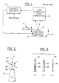
- FIG. 1 A block diagram of an AFM using interferometric laser detection is shown in Fig. 1, with a probe arrangement 10 being emplaced over the surface of specimen 12. Changes in oscillation amplitude of probe arrangement 10 are sensed by a laser heterodyne interferometer 14 that provides an output signal to a feedback generator 16. As an output signal changes with respect to an applied reference signal, feedback generator 16 provides position control signals to a piezoelectric position control unit 18. Those control signals cause a piezoelectric unit within position control element 18 to move the specimen so that the vibration amplitude is stabilized and, hence the the force gradient. The fluctuations in the feedback potential are converted into a profile of the surface being investigated.
- AFM electrostatic-force microscope
- the vibrating probe bears an electric charge and its vibration amplitude is effected by electrostatic forces resulting from charges in the sample.
- AFM Magnetic-force microscope
- MFM magnetic-force microscope
- a magnetized nickel or iron probe is substituted for the tungsten or silicon needles used with other AFM's.
- the tip feels a magnetic force that changes its resonance frequency and hence its vibration amplitude.
- the MFM traces magnetic-field patterns emanating from the specimen.
- the magnetic force components sensed by an MFM probe result from the interaction of the total magnetic dipole moments at the tip of the probe and the specimen. They are further dependent upon the influence of tip-related magnetic fields on the local magnetic moments of the specimen.
- the lateral resolution of the probe depends critically on the interaction volume constituted by the sample and the tip. For planar magnetic media, this interaction volume is determined primarily by geometric and magnetic properties of the probe tip. Thus, in order to obtain lateral resolutions below 100,0 nm, current tip sizes in the range of 100,0 nm are too large.
- magnetic sensor probe tips are fabricated by an electrochemical etching technique using a ferromagnetic wire material (such as nickel, iron, or cobalt). Essentially the method comprises etching the tip of the wire until it approximates a point. This method does not provide control over the geometric shape of the tip below a 100,0 nm radius. Such probe tips, further, have an unnecessarily large amount of magnetic material with a complicated domain structure. In essence, subtractive processes for creating MFM and other AFM probe tips, do not today, provide the desired atomic-level resolution capability.
- a ferromagnetic wire material such as nickel, iron, or cobalt
- a film is deposited on a semiconductor substrate by passing a gas containing an element over the substrate and then irradiating a determined portion thereof with an electron beam. The gas decomposes and the element is precipitated onto the substrate so as to form a desired pattern. Chromium, molybdenum, aluminum, and tungsten containing organometallics are disclosed. In Japanese Patent 87-295,886/42 the use of organometallic compounds is described for producing a film of VIII metals on a substrate. Electron beams have also been used to enable surface analysis of substrates (e.g., see Kuptsis, IBM Technical Disclosure Bulletin, Vol. 13, No. 9, February 1971, pp. 2497-2498).
- a probe tip for a scanned probe microscope is configured as a needle extending from a surface, the needle further comprising a carbonized matrix of a decomposed organic reactant.
- the needle exhibits a substantial stiffness along its elongated dimension and has a nanometer scale tip dimension.
- a method is described for producing such a needle probe tip wherein a substrate is positioned in an evacuated environment; a volatile organic compound is introduced into the environment and an energy beam, for example a laser beam, an electron beam or an x-ray beam from a synchrotron and the like, is directed at the substrate's surface, which energy beam is maintained stably focussed thereon for a preset time period.
- the beam causes a selective decomposition of the organic compound at the focal point on the substrate surface and causes succeeding layers of decomposition product of the organic compound to grow directly up the beam, to thus produce a substantially rigid nanometer-scale needle-like form.
- a magnetic layer is then deposited on the top of the structure, such layer having a dimension which restricts the tip to exhibit a single magnetic domain.
- FIG. 2 the structure of an AFM nanometer scale needle probe will be described, including the process for producing such a probe.
- a substrate 20 is placed in an evacuated chamber within an electron beam unit.
- substrate 20 is a silicon cone.
- a volatile, organometallic compound gas stream is then introduced into the subchamber 64, while at the same time, an electron beam 22 is turned on. Beam 22 impinges upon an upper surface 24 of substrate 20 and causes decomposition and preferential deposition of the decomposed products of the organometallic gas onto surface 24. Such deposition occurs within the region irradiated by electron beam 22 and also out therefrom by a radial distance determined by electron scatter from surface 24. If it is assumed that electron beam 22 has a diameter of 6 nanometers, the diameter of the initial deposit is approximately 100 nanometers. As the process continues, additional layers of deposited, decomposed components of the organometallic gas continue to build up, thereby creating a needle-like shape 26.
- a conical tip shape for needle 26 and its shank diameter are achieved by control of the primary beam voltage and also the beam's gaussian profile.
- the needle diameter and the respective cone apex angle decrease with increasing beam voltage ( ⁇ 10% for a 10 kV increase).
- Such a needle shape is shown in Fig. 3(a).
- the apparent diameter of pointed end 28 of needle 26 can be made approximately 10 nanometers.
- the process employed to deposit needle probe 26 onto a substrate is an electron beam chemical vapor deposition (CVD) process.
- CVD electron beam chemical vapor deposition
- Such processes, per se, are known in the prior art, e.g., see Japanese Patent 87-295,886/42. Nevertheless, to Applicants' knowledge, such processes have not heretofore been employed to produce nanometer scale, needle-like structures having a high aspect ratio.
- the E-beam CVD process produces a needle probe which exhibits substantial stiffness along its elongated dimension. It is believed that this rigidity results from the CVD process producing a needle with a carbon matrix structure in which metal particles are dispersed. In other words, the included carbon toughens the structure and makes it usable as an AFM probe. Without such structural stiffness, needle probe 26 would be useless as an AFM probe.
- metal carbonyls or metal alkyls can be employed as organometallic source compounds for the CVD process, it is preferred that metallocenes be employed due to the non-thermal, decomposition process occuring under e-beam irradiation.
- metallocenes be employed due to the non-thermal, decomposition process occuring under e-beam irradiation.
- cobaltocene, nickelocene, and/or ferrocene are preferred.
- a needle structure such as shown in Fig. 3(a) is grown and exhibits intrinsic, but weak, magnetic capabilities.
- Such needle structure comprises a carbon matrix with nickel, cobalt or iron particles, as the case may be, dispersed therein.
- a seeding step followed by a plate-up of a magnetic material.
- a seeding material e.g., allycyclopentadienylpalladium
- a seeding material is used to grow needle 26 (see Fig. 3(b)). This results in a non-magnetic needle structure having palladium seed particles interspersed.
- the entire surface of needle 26 is then covered, in a subsequent electroless plating process, by a magnetic metal layer 30.
- the needle 26 is grown without an included metal component. Then a seeding material 32 is deposited only on the apex of needle 26. This is accomplished by introduction of a gaseous metallorganic containing the seed metal, followed by electron beam exposure of the tip area. A subsequent plating (e.g. selective CVD in a gaseous or liquid environment) of a magnetic metal 30 will therefore be confined to the seeded area at the apex and will yield a single domain magnetic sensor region for needle probe 26.
- a seeding material 32 is deposited only on the apex of needle 26. This is accomplished by introduction of a gaseous metallorganic containing the seed metal, followed by electron beam exposure of the tip area.
- a subsequent plating (e.g. selective CVD in a gaseous or liquid environment) of a magnetic metal 30 will therefore be confined to the seeded area at the apex and will yield a single domain magnetic sensor region for needle probe 26.
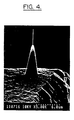
- Fig. 4 a perspective view taken from an SEM photograph is shown wherein a 3 micron long needle probe with a 100 nanometer shank diameter was produced using the method of this invention.
- the substrate is a silicon pedestal produced via selective etching.
- Silicon probe tips such as tip 20 shown in Fig. 2 or the one shown in Fig. 4, are produced by microfabrication techniques that are known in the art. For instance, see Albrecht et al., "Microfabrication of Cantilever Styli for the Atomic Force Microscope", Journal of Vacuum Science Technology, A8(4), July/August 1990, pp. 3386-3396. In that reference and in the references cited therein, techniques are described for selective etching of silicon substrates to enable the creation of an AFM cantilever with an integral pointed silicon probe tip. The procedures used to provide such integral cantilever/probe structures employ selective etching and mask undercutting to enable production of the probe tips. The Albrecht et al. article also describes methods for fabricating thin film SiO2 and Si3N4 microcantilevers having integral probe tips. Such procedures do not form a part of this invention, although they do provide the methods and procedures whereby an appropriate support surface for the needle probe of this invention can be produced.
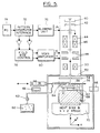
- a direct E-beam deposition system comprises a modified scanning electron microscope.
- the column portion of the microscope includes a filament 40 which is preferably a lanthanum boride electron source.
- a movable anode structure 42 is provided to enable the beam brightness to be optimized.
- the beam passes through a pair of condenser lenses 44, 46, double deflection coils 48 and a final lens 50. From there, the beam enters a lower chamber 52, passes through a backscatter electron detector 54 and then passes into and through a retractable shutter arrangement 56.
- a linear drive mechanism 59 controls the position of the retractable shutter.
- the shutter is closed and the beam passes through a pin hole therein (not shown).
- a pin hole therein not shown.
- Substrate 58 is positioned in subchamber 64 and on a Peltier effect heater/cooler 60 which maintains constant its temperature.
- a vapor source 62 provides a vapor of an organometallic containing gas into subchamber 64.
- a capacitance manometer 66 maintains the pressure within subchamber 64 within desired limits.
- Various detection systems are included, including a secondary electron detector 66 and a STEM detector 68.
- the position of substrate 58 is controlled by an XYZ stage 70 and controls that enable the discrete positioning of stage 70 (not shown).
- the deposition system is interfaced to a pattern generating unit 72 which is controlled by a personal computer 74 to vector position the electron beam onto the substrate.
- Electron beam on-time is controlled by an electrostatic blanking unit 76.
- the exposure time per pixel ranges from 1 microsecond to greater than 100 seconds. For a 50X50 micron field, a beam step size of approximately 5 nanometers can be obtained with 14 bit digital to analog conversion.
- Such control is exerted by field size control unit 78 through scan control amplifiers 80.
- a source gas is introduced from vapor source 62 through a metering needle valve 63 into subchamber 64 within lower chamber 52.
- Subchamber 64 is differentially pumped to an operating pressure range of 10-100 m Torr.
- Such pressures are compatible with the available beam current densities, and enable optimum growth in the E-beams CVD process.
- Typical pressure in SEM chamber 52 is approximately 133,3 ⁇ 10 ⁇ 4 N m2 (10 ⁇ 4 Torr) and the pressure in the gun area which encompasses source 40 is approximately 133,3 ⁇ 10 ⁇ 7 N m2 (10 ⁇ 7 Torr).
- a weak magnetic probe needle comprised of nickel embedded in a carbon matrix, having a shank diameter of approximately 100 nanometers and length of two microns was deposited on a silicon substrate.
- the organometallic gas used for this example was a nickelocene complex at a vapor pressure of 5 mTorr in subchamber 64.
- the substrate temperature was 20°C
- the beam voltage was 30 kV
- the beam size diameter was approximately 6 nanometers.
- the exposure time was between 5 and 10 minutes.
- a strong magnetic needle sensor was produced under the following experimental conditions: A needle was first grown under same beam conditions and temperature as described above, using allycyclopentadienylpalladium complex as the vapor source material. Subsequently, the needle surface was plated in an electroless NiSO4 solution at 65°C yielding ⁇ 10nm nickel coverage in 5 seconds.
- the above-described E-beam deposition process when applied to the deposition of a three-dimensional needle-like structure, has the unique characteristic of enabling monolayer film thickness control, high resolution, and the production of a high aspect ratio structure (i.e., more than 31). For most applications, it will probably be advantageous to produce an elongated magnetic tip shape, which would guarantee that the tip be magnetized along its long axis. Given the nanometer scale tip dimension, a single domain probe tip is achieved, enabling imaging of magnetic structures in the sample surface with atomic level resolution.
Landscapes
- Physics & Mathematics (AREA)
- General Physics & Mathematics (AREA)
- Health & Medical Sciences (AREA)
- General Health & Medical Sciences (AREA)
- Nuclear Medicine, Radiotherapy & Molecular Imaging (AREA)
- Radiology & Medical Imaging (AREA)
- Chemical & Material Sciences (AREA)
- Engineering & Computer Science (AREA)
- Nanotechnology (AREA)
- Measurement Of Length, Angles, Or The Like Using Electric Or Magnetic Means (AREA)
- Length Measuring Devices With Unspecified Measuring Means (AREA)
- Measuring Magnetic Variables (AREA)
Description
- This invention relates to atomic force microscopy, and more particularly, to a nanometer scale probe for use with an atomic force microscope.
- Scanned probe microscopy saw its commencement at the atomic level with the invention by Binnig et al. of the scanning tunnelling microscope in the mid-1980's. In the scanning tunnelling microscope (STM), a tiny tungsten probe is maneuvered to within a nanometer above the surface of a conducting specimen, sufficiently close so that there is an overlap between the electron clouds of the atom at the probe tip and of the nearest atom of the specimen. When a small voltage is applied to the tip, electrons "tunnel" across the gap generating a small tunnelling current. The strength of that current is very sensitive to the width of the gap. Piezoelectric controls are used to control the motion of the probe and move it back and forth across the specimen while maintaining a constant gap between its tip and the specimen surface. The variations in voltage applied to maintain the probe properly positioned over the surface are electronically translated into an image of the surface topography.
- The invention of STM has led to the development of a family of new scanned-probe microscopes, one of which is the atomic force microscope (AFM) which negates the need for a conducting specimen. In its first implementation, the AFM relied upon the repulsive forces generated by the overlap of the electron cloud at the tip's surface with electron clouds of surface atoms within the specimen. The tip is mounted on a flexible beam which maintains the tip pressed against the specimen surface with constant force as it is moved across the surface.
- While a number of methods have been used to measure the movement of the AFM beam/tip, more recently, this is done by a laser beam. The reflected laser is detected and enables beam movements to be converted to imaging signals.
- A more recent development is an AFM that is based on the detection of an attractive force between a surface and a probe by its effect on the dynamics of a vibrating probe/beam arrangement. Commonly in such arrangements, a tapered tungsten wire is driven by a piezoelectric transducer mounted at its base to vibrate at close to the wire's resonant frequency. As the tip of the wire is moved across a surface, amplitude changes occur in the vibration as a result of the attractive forces. The changes in the vibration amplitude are sensed by an interferometric laser arrangement.
- A block diagram of an AFM using interferometric laser detection is shown in Fig. 1, with a
probe arrangement 10 being emplaced over the surface ofspecimen 12. Changes in oscillation amplitude ofprobe arrangement 10 are sensed by alaser heterodyne interferometer 14 that provides an output signal to afeedback generator 16. As an output signal changes with respect to an applied reference signal,feedback generator 16 provides position control signals to a piezoelectricposition control unit 18. Those control signals cause a piezoelectric unit withinposition control element 18 to move the specimen so that the vibration amplitude is stabilized and, hence the the force gradient. The fluctuations in the feedback potential are converted into a profile of the surface being investigated. - Another variation of the AFM within which the invention can be used is the electrostatic-force microscope where the vibrating probe bears an electric charge and its vibration amplitude is effected by electrostatic forces resulting from charges in the sample. One form of AFM is a magnetic-force microscope (MFM). In an MFM, a magnetized nickel or iron probe is substituted for the tungsten or silicon needles used with other AFM's. When the vibrating probe is brought near a magnetic sample, the tip feels a magnetic force that changes its resonance frequency and hence its vibration amplitude. The MFM traces magnetic-field patterns emanating from the specimen.
- The magnetic force components sensed by an MFM probe result from the interaction of the total magnetic dipole moments at the tip of the probe and the specimen. They are further dependent upon the influence of tip-related magnetic fields on the local magnetic moments of the specimen. The lateral resolution of the probe depends critically on the interaction volume constituted by the sample and the tip. For planar magnetic media, this interaction volume is determined primarily by geometric and magnetic properties of the probe tip. Thus, in order to obtain lateral resolutions below 100,0 nm, current tip sizes in the range of 100,0 nm are too large.
- Recent theoretical calculations by Wadas in the Journal of Magnetism and Magnetic Materials, Vol. 71, p. 147 (1988) and Vol. 72, p. 292 (1988) show that even for probe tip sizes below 100,0 nm, detection sensitivity of the magnetic forces can be greatly improved by optimization of probe tip shape. Those calculations suggest that only the first 10,0 nm of magnetic material at the tip are effective in contributing to magnetic force interactions that yield high resolution information. The remainder of the magnetic material at the probe tip contributes a background force due to long-range interactions between the magnetic cantilever and the specimen. These interactions are detrimental to sensitivity and spatial resolution and may induce domain wall motion in soft magnetic materials and instability in the tip-to-specimen separation.
- Currently, magnetic sensor probe tips are fabricated by an electrochemical etching technique using a ferromagnetic wire material (such as nickel, iron, or cobalt). Essentially the method comprises etching the tip of the wire until it approximates a point. This method does not provide control over the geometric shape of the tip below a 100,0 nm radius. Such probe tips, further, have an unnecessarily large amount of magnetic material with a complicated domain structure. In essence, subtractive processes for creating MFM and other AFM probe tips, do not today, provide the desired atomic-level resolution capability.
- The prior art is replete with many additive techniques for deposition of both magnetic and nonmagnetic materials. High energy electron and laser beams are also used to enhance local deposition of materials onto a surface from a gaseous environment. Those systems generally are employed to deposit a pattern onto a substrate, such pattern derived by selective deposition of one or more components of the gaseous environment through which the energy beam is being directed. In U.S. Patent 4,382,186 to Denholm et al., a process is described which employs finely focussed electron beams to effect physical, chemical and other changes on the surface of a substrate. In U.S. Patent 4,670,291 to Mori et al. the injection of exotic atoms into a semiconductor substrate is achieved through the use of an electron beam irradiation scheme.
- In U.S. Patent 4,605,566 to Matsui et al., a film is deposited on a semiconductor substrate by passing a gas containing an element over the substrate and then irradiating a determined portion thereof with an electron beam. The gas decomposes and the element is precipitated onto the substrate so as to form a desired pattern. Chromium, molybdenum, aluminum, and tungsten containing organometallics are disclosed. In Japanese Patent 87-295,886/42 the use of organometallic compounds is described for producing a film of VIII metals on a substrate. Electron beams have also been used to enable surface analysis of substrates (e.g., see Kuptsis, IBM Technical Disclosure Bulletin, Vol. 13, No. 9, February 1971, pp. 2497-2498).
- More recently, it has been found that iron, nickel, and palladium may be deposited on silicon directly from metallocenes. This is in contrast to other energy-beam assisted deposition systems wherein metal carbonyls and metal alkyls are employed as organometallic source compounds. Such actions are described by Stauf et al. in "Patterned Photo Assisted Organometallic metallic Deposition of Iron, Nickel and Palladium on Silicon", Thin Solid Films, 156 (1988) pp. L31-L36. In specific, Stauf et al. indicate that depositions of metals from the decomposition of cobaltocene, nickelocene, and ferrocene were achieved by both conventional pyrolysis and by single-photon (non-thermal) photodecomposition or plasma-assisted deposition. Photo assisted deposition, as well as electron beam deposition, are essentially non-thermal in character.
- In Journal of Vacuum Science and Technology 8(1990) January/February, No. 1, N.Y., pages 429 to 433 electron-beam deposition inside scanning electron microscope (SEM) is used to prepare a new scanning tunneling microscope (STM) tip, an electron-beam deposited (EBD) tip, which has a submicron diameter and a long straight sidewall. An EBD tip as small as less than 0.1 »m in diameter can be formed with careful beam focusing. This EBD tip is formed to be capable of providing a low-distortion STM image of deep grooves, and is quite useful in topographic measurements of microfabricated patterns. In Applied Physics Letters vol. 56, no. 20, 14 May 1990, pages 2045 to 2047 a simple technique for preparing magnetic tips used in a scanning force microscope is described. In this technique a thin layer of ferromagnetic material is deposited on an etched tungsten tip via sputtering or galvanic deposition. Images of magnetic domains obtained with these tips are presented, demonstrating a lateral resolution of the order of 50-100 nm.
- Accordingly, it is the object of this invention to disclose a new and advantageous process for producing an AFM probe tip.
- According to the present invention as claimed a probe tip for a scanned probe microscope is configured as a needle extending from a surface, the needle further comprising a carbonized matrix of a decomposed organic reactant. The needle exhibits a substantial stiffness along its elongated dimension and has a nanometer scale tip dimension. A method is described for producing such a needle probe tip wherein a substrate is positioned in an evacuated environment; a volatile organic compound is introduced into the environment and an energy beam, for example a laser beam, an electron beam or an x-ray beam from a synchrotron and the like, is directed at the substrate's surface, which energy beam is maintained stably focussed thereon for a preset time period. The beam causes a selective decomposition of the organic compound at the focal point on the substrate surface and causes succeeding layers of decomposition product of the organic compound to grow directly up the beam, to thus produce a substantially rigid nanometer-scale needle-like form. A magnetic layer is then deposited on the top of the structure, such layer having a dimension which restricts the tip to exhibit a single magnetic domain.
- For a better understanding of the present invention, together with further objects and advantages, preferred embodiment of the invention are described in the following with reference to the accompanying drawings, in which:
- Fig. 1
- is a block diagram showing a scanned-probe microscope of the prior art.
- Fig. 2
- is a schematic, perspective view of a silicon probe on which a nanometer-scale needle probe is grown in accordance with the invention.
- Figs. 3(a)-(c)
- show three separate versions of the nanometer-scale needle of this invention.
- Fig. 4
- is a reproduction of a photomicrograph showing a nanometer-scale needle produced on a silicon probe tip in accordance with this invention.
- Fig. 5
- is a schematic view of a modified scanning electron microscope used to implement the method of this invention.
- Referring now to Fig. 2, the structure of an AFM nanometer scale needle probe will be described, including the process for producing such a probe.
- Initially, a
substrate 20 is placed in an evacuated chamber within an electron beam unit. In this example,substrate 20 is a silicon cone. A volatile, organometallic compound gas stream is then introduced into thesubchamber 64, while at the same time, anelectron beam 22 is turned on.Beam 22 impinges upon anupper surface 24 ofsubstrate 20 and causes decomposition and preferential deposition of the decomposed products of the organometallic gas ontosurface 24. Such deposition occurs within the region irradiated byelectron beam 22 and also out therefrom by a radial distance determined by electron scatter fromsurface 24. If it is assumed thatelectron beam 22 has a diameter of 6 nanometers, the diameter of the initial deposit is approximately 100 nanometers. As the process continues, additional layers of deposited, decomposed components of the organometallic gas continue to build up, thereby creating a needle-like shape 26. - A conical tip shape for
needle 26 and its shank diameter are achieved by control of the primary beam voltage and also the beam's gaussian profile. In general, the needle diameter and the respective cone apex angle decrease with increasing beam voltage (∩10% for a 10 kV increase). Such a needle shape is shown in Fig. 3(a). It has also been found, with appropriate controls, that the apparent diameter ofpointed end 28 ofneedle 26 can be made approximately 10 nanometers. Whenneedle 26 is constructed to exhibit magnetic characteristics, a 10 nanometer tip diameter will restrict the magnetic action thereat to a single domain, thereby avoiding the aforestated problems which arise from long range magnetic field line intercouplings. - The process employed to deposit
needle probe 26 onto a substrate is an electron beam chemical vapor deposition (CVD) process. Such processes, per se, are known in the prior art, e.g., see Japanese Patent 87-295,886/42. Nevertheless, to Applicants' knowledge, such processes have not heretofore been employed to produce nanometer scale, needle-like structures having a high aspect ratio. It has further been found that the E-beam CVD process produces a needle probe which exhibits substantial stiffness along its elongated dimension. It is believed that this rigidity results from the CVD process producing a needle with a carbon matrix structure in which metal particles are dispersed. In other words, the included carbon toughens the structure and makes it usable as an AFM probe. Without such structural stiffness,needle probe 26 would be useless as an AFM probe. - While metal carbonyls or metal alkyls can be employed as organometallic source compounds for the CVD process, it is preferred that metallocenes be employed due to the non-thermal, decomposition process occuring under e-beam irradiation. To produce a needle probe having intrinsic magnetic characteristics, cobaltocene, nickelocene, and/or ferrocene are preferred. In such case, a needle structure such as shown in Fig. 3(a) is grown and exhibits intrinsic, but weak, magnetic capabilities. Such needle structure comprises a carbon matrix with nickel, cobalt or iron particles, as the case may be, dispersed therein.
- For applications requiring a more strongly magnetic tip on the needle probe, different growth conditions should be employed involving at least two processing steps: a seeding step followed by a plate-up of a magnetic material. Among various alternative methods, two are preferred. In the first method a seeding material (e.g., allycyclopentadienylpalladium) is used to grow needle 26 (see Fig. 3(b)). This results in a non-magnetic needle structure having palladium seed particles interspersed. The entire surface of
needle 26 is then covered, in a subsequent electroless plating process, by amagnetic metal layer 30. - In the second method (see Fig. 3(c)) the
needle 26 is grown without an included metal component. Then a seedingmaterial 32 is deposited only on the apex ofneedle 26. This is accomplished by introduction of a gaseous metallorganic containing the seed metal, followed by electron beam exposure of the tip area. A subsequent plating (e.g. selective CVD in a gaseous or liquid environment) of amagnetic metal 30 will therefore be confined to the seeded area at the apex and will yield a single domain magnetic sensor region forneedle probe 26. - In Fig. 4, a perspective view taken from an SEM photograph is shown wherein a 3 micron long needle probe with a 100 nanometer shank diameter was produced using the method of this invention. The substrate is a silicon pedestal produced via selective etching.
- Silicon probe tips such as
tip 20 shown in Fig. 2 or the one shown in Fig. 4, are produced by microfabrication techniques that are known in the art. For instance, see Albrecht et al., "Microfabrication of Cantilever Styli for the Atomic Force Microscope", Journal of Vacuum Science Technology, A8(4), July/August 1990, pp. 3386-3396. In that reference and in the references cited therein, techniques are described for selective etching of silicon substrates to enable the creation of an AFM cantilever with an integral pointed silicon probe tip. The procedures used to provide such integral cantilever/probe structures employ selective etching and mask undercutting to enable production of the probe tips. The Albrecht et al. article also describes methods for fabricating thin film SiO₂ and Si₃N₄ microcantilevers having integral probe tips. Such procedures do not form a part of this invention, although they do provide the methods and procedures whereby an appropriate support surface for the needle probe of this invention can be produced. - Turning now to Fig. 5, a direct E-beam deposition system is shown and comprises a modified scanning electron microscope. The column portion of the microscope includes a
filament 40 which is preferably a lanthanum boride electron source. Amovable anode structure 42 is provided to enable the beam brightness to be optimized. The beam passes through a pair ofcondenser lenses final lens 50. From there, the beam enters alower chamber 52, passes through abackscatter electron detector 54 and then passes into and through aretractable shutter arrangement 56. Alinear drive mechanism 59 controls the position of the retractable shutter. - During the period when deposition is occurring, the shutter is closed and the beam passes through a pin hole therein (not shown). When the shutter is open, high resolution secondary electron and scanning transmission imaging can be carried out for probe size monitoring and residual astigmatism correction.
-
Substrate 58 is positioned insubchamber 64 and on a Peltier effect heater/cooler 60 which maintains constant its temperature. Avapor source 62 provides a vapor of an organometallic containing gas intosubchamber 64. Acapacitance manometer 66 maintains the pressure withinsubchamber 64 within desired limits. Various detection systems are included, including asecondary electron detector 66 and aSTEM detector 68. The position ofsubstrate 58 is controlled by anXYZ stage 70 and controls that enable the discrete positioning of stage 70 (not shown). - The deposition system is interfaced to a
pattern generating unit 72 which is controlled by apersonal computer 74 to vector position the electron beam onto the substrate. Electron beam on-time is controlled by anelectrostatic blanking unit 76. The exposure time per pixel ranges from 1 microsecond to greater than 100 seconds. For a 50X50 micron field, a beam step size of approximately 5 nanometers can be obtained with 14 bit digital to analog conversion. Such control is exerted by fieldsize control unit 78 throughscan control amplifiers 80. - For direct E-beam deposition, a source gas is introduced from
vapor source 62 through ametering needle valve 63 intosubchamber 64 withinlower chamber 52.Subchamber 64 is differentially pumped to an operating pressure range of 10-100 m Torr. Such pressures are compatible with the available beam current densities, and enable optimum growth in the E-beams CVD process. Typical pressure inSEM chamber 52 is approximately
source 40 is approximately
- As the E-beam CVD process is considerably less sensitive than other resist-based processes, relatively long exposure times are required. Such times demand high stability from the electron-optical column and the substrate stage. For the above-noted SEM column, no noticable beam drift was observed and the measured beam current variation over an exposure time of two hours was approximately 5%. The major source of drift was found to occur in the microscope stage where sample cooling caused thermal stresses in the stage assembly. The problem was corrected by providing sufficient heat sinking to
subchamber 52. In this manner, sample temperature variation was kept within 1°C, without noticable drift in substrate position. - Using the E-beam system shown in Fig. 5, a weak magnetic probe needle comprised of nickel embedded in a carbon matrix, having a shank diameter of approximately 100 nanometers and length of two microns was deposited on a silicon substrate. The organometallic gas used for this example was a nickelocene complex at a vapor pressure of 5 mTorr in
subchamber 64. The substrate temperature was 20°C, the beam voltage was 30 kV and the beam size diameter was approximately 6 nanometers. The exposure time was between 5 and 10 minutes. - A strong magnetic needle sensor was produced under the following experimental conditions: A needle was first grown under same beam conditions and temperature as described above, using allycyclopentadienylpalladium complex as the vapor source material. Subsequently, the needle surface was plated in an electroless NiSO₄ solution at 65°C yielding ∼10nm nickel coverage in 5 seconds.
- The above-described E-beam deposition process, when applied to the deposition of a three-dimensional needle-like structure, has the unique characteristic of enabling monolayer film thickness control, high resolution, and the production of a high aspect ratio structure (i.e., more than 31). For most applications, it will probably be advantageous to produce an elongated magnetic tip shape, which would guarantee that the tip be magnetized along its long axis. Given the nanometer scale tip dimension, a single domain probe tip is achieved, enabling imaging of magnetic structures in the sample surface with atomic level resolution.
- It should be understood that the foregoing description is only illustrative of the invention. Various alternatives and modifications can be devised by those skilled in the art without departing from the invention. For instance, while it is preferred that an organometallic be used to create the needle-like structure, an organic gas can be employed to grow a carbonized, non-metal needle structure, which is then seeded via deposition of a seed layer, followed by a magnetic metal deposition from a metallocene vapor. Accordingly, the present invention is intended to embrace all such alternatives, modifications and variances which fall within the scope of the appended claims.
Claims (13)
- A probe for a scanned-probe microscope, comprising:
a substrate (20, 58);
a nanometer scale, needle-shaped structure (26) having an apex (28), exhibiting a high aspect ratio, extending from said substrate, said structure comprising a carbonized material, said structure further exhibiting a substantial stiffness, characterized in that said carbonized material comprises a carbonized matrix of a decomposed organic reactant and that said needle-shaped structure has a single magnetic domain at said apex. - The probe as recited in claim 1 wherein said carbonized matrix includes metallic deposits interspersed therein.
- The probe as recited in claim 2 wherein said metallic deposits exhibit magnetic properties.
- The probe as recited in claim 3 wherein said structure exhibits a tip diameter sufficiently small that it manifests the single magnetic domain thereat.
- The probe as recited in claim 1 wherein said substrate comprises a flexible cantilever having an integral protrusion extending in a perpendicular direction therefrom said protrusion having apex surface (24) from which said needle-like structure (26) extends.
- The probe as recited in claim 5 wherein said flexible cantilever and protrusion are comprised of a silicon-based material.
- The probe as recited in claim 1 further comprising: a thin metal layer disposed on at least a distal end of said structure, said thin metal layer exhibiting magnetic properties.
- The probe as recited in claim 7 further comprising:
a thin metal-containing interlayer disposed between said distal end of said structure and said thin metal magnetic layer. - The probe as recited in any of the preceding claims 1 to 8, wherein said needle-shaped structure has an aspect ratio of greater than about 10 to 1.
- A method for producing a probe for a scanned probe microscope, said probe comprising a substrate (20, 58) and a supported probe tip (28), the method comprising:
positioning said substrate (20, 58) in an evacuated environment;
introducing a volatile, gaseous, organic-based compound into said environment, wherein said organic-based compound contains a seeding metal,
directing an energy beam at said substrate and stably maintaining said beam focused at a point thereon for a set time period, said beam causing decomposition of said organic compound at said point where said beam is incident on said substrate, whereby succeeding layers of decomposition product of said organic-based compound are enable to grow from said substrate in the direction of said beam, to thereby produce a rigid, high aspect ratio, nanometer scale, tip structure;
depositing a metal layer on the surface of said high aspect ratio structure, wherein said metal layer exhibits magnetic properties and has a dimension which restricts said tip to exhibit a single magnetic domain. - The method of claim 10 wherein said energy beam is a beam of electrons (22).
- The method of claim 11, wherein the geometrical details of said tip structure is controlled by beam size and incident beam energy of said beam of electrons.
- The method of any one of claims 10 to 12, wherein said volatile organic compound is chosen from the class of metallocenes.
Applications Claiming Priority (2)
| Application Number | Priority Date | Filing Date | Title |
|---|---|---|---|
| US608043 | 1984-05-07 | ||
| US60804390A | 1990-10-31 | 1990-10-31 |
Publications (3)
| Publication Number | Publication Date |
|---|---|
| EP0483579A2 EP0483579A2 (en) | 1992-05-06 |
| EP0483579A3 EP0483579A3 (en) | 1992-12-30 |
| EP0483579B1 true EP0483579B1 (en) | 1995-12-27 |
Family
ID=24434783
Family Applications (1)
| Application Number | Title | Priority Date | Filing Date |
|---|---|---|---|
| EP91117499A Expired - Lifetime EP0483579B1 (en) | 1990-10-31 | 1991-10-14 | Nanometer scale probe for an atomic force microscope, and method for making the same |
Country Status (3)
| Country | Link |
|---|---|
| EP (1) | EP0483579B1 (en) |
| JP (1) | JPH081382B2 (en) |
| DE (1) | DE69115847T2 (en) |
Cited By (1)
| Publication number | Priority date | Publication date | Assignee | Title |
|---|---|---|---|---|
| US7608147B2 (en) | 2003-04-04 | 2009-10-27 | Qunano Ab | Precisely positioned nanowhiskers and nanowhisker arrays and method for preparing them |
Families Citing this family (23)
| Publication number | Priority date | Publication date | Assignee | Title |
|---|---|---|---|---|
| DE4239532C1 (en) * | 1992-11-25 | 1994-02-10 | Kernforschungsz Karlsruhe | Use of micro carbon fibers |
| US5321977A (en) * | 1992-12-31 | 1994-06-21 | International Business Machines Corporation | Integrated tip strain sensor for use in combination with a single axis atomic force microscope |
| DE4314301C1 (en) * | 1993-04-30 | 1994-05-05 | Imm Inst Mikrotech | Surface scanning sensor - has a sensor point of a photo-structurable glass |
| IL113551A0 (en) * | 1995-04-30 | 1995-07-31 | Fish Galina | Tapered structure suitable for microthermocouples microelectrodes field emission tips and micromagnetic sensors with force sensing capabilities |
| DE19519478C2 (en) * | 1995-05-27 | 1997-09-04 | Forschungszentrum Juelich Gmbh | Manufacturing method for coated tip probe |
| JP2000516708A (en) | 1996-08-08 | 2000-12-12 | ウィリアム・マーシュ・ライス・ユニバーシティ | Macroscopically operable nanoscale devices fabricated from nanotube assemblies |
| DE19718478C2 (en) * | 1997-04-30 | 2003-05-28 | Allice Mestechnik Gmbh | High impedance probe with extremely small input capacitance |
| CA2336531A1 (en) * | 1998-07-08 | 2000-01-20 | Capres Aps | Multi-point probe |
| EP1698905B9 (en) * | 1999-09-15 | 2012-01-18 | Capres A/S | Nano-drive for high resolution positioning and for positioning of a multi-point probe |
| US7032437B2 (en) * | 2000-09-08 | 2006-04-25 | Fei Company | Directed growth of nanotubes on a catalyst |
| JP4688400B2 (en) * | 2001-12-04 | 2011-05-25 | エスアイアイ・ナノテクノロジー株式会社 | Probe for scanning probe microscope |
| JP4858924B2 (en) * | 2001-12-04 | 2012-01-18 | エスアイアイ・ナノテクノロジー株式会社 | Creating a probe for a scanning probe microscope |
| KR20060058085A (en) * | 2003-07-08 | 2006-05-29 | 큐나노 에이비 | Probe structures incorporating nanowhiskers, methods of making the same, and methods of forming nanowhiskers |
| DE10342644A1 (en) * | 2003-09-16 | 2005-04-07 | Nanotools Gesellschaft für Spezialanwendungen in der Rastersondenmikroskopie mbH | Raster force microscopy probe has nano structure probe tip arm with integrated CMOS piezoelectric sensor |
| US7553335B2 (en) | 2004-04-23 | 2009-06-30 | Japan Science And Technology Agency | Scanning probe microscope probe and manufacturing method therefor, scanning probe microscope and using method therefor, needle-like body and manufacturing method therefor, electronic device and manufacturing method therefor, charge density wave quantum phase microscope, and charge density wave quantum interferometer |
| JP2005308652A (en) * | 2004-04-23 | 2005-11-04 | Japan Science & Technology Agency | Probe microscope probe and method for manufacturing the same, probe microscope, needle-shaped body and method for manufacturing the same, electronic device and method for manufacturing the same |
| US7370515B2 (en) | 2004-06-21 | 2008-05-13 | Veeco Instruments Inc. | Probes for use in scanning probe microscopes and methods of fabricating such probes |
| JP2006125984A (en) | 2004-10-28 | 2006-05-18 | Japan Science & Technology Agency | Measuring device with daisy type cantilever wheel |
| DE102005063127B3 (en) * | 2005-12-30 | 2007-08-23 | Universität Hamburg | Micro and nano tips and methods for their production |
| DE102006008858B4 (en) * | 2006-02-25 | 2016-10-20 | Nanotools Gmbh | probe means |
| JP4806762B2 (en) * | 2006-03-03 | 2011-11-02 | 国立大学法人 名古屋工業大学 | SPM cantilever |
| CN106597035A (en) * | 2016-11-18 | 2017-04-26 | 武汉新芯集成电路制造有限公司 | Nanoprobe and nanoprobe tester |
| CN112723306B (en) * | 2020-12-17 | 2023-08-18 | 武汉光谷航天三江激光产业技术研究院有限公司 | Atomic air chamber manufacturing integrated bonding device and method for alkali metal direct filling |
Family Cites Families (2)
| Publication number | Priority date | Publication date | Assignee | Title |
|---|---|---|---|---|
| US4605566A (en) * | 1983-08-22 | 1986-08-12 | Nec Corporation | Method for forming thin films by absorption |
| EP0437275B1 (en) * | 1990-01-11 | 1997-08-27 | Canon Kabushiki Kaisha | Microprobe, method for producing the same, and information input and/or output apparatus utilizing the same |
-
1991
- 1991-08-27 JP JP3238905A patent/JPH081382B2/en not_active Expired - Fee Related
- 1991-10-14 DE DE69115847T patent/DE69115847T2/en not_active Expired - Fee Related
- 1991-10-14 EP EP91117499A patent/EP0483579B1/en not_active Expired - Lifetime
Non-Patent Citations (1)
| Title |
|---|
| microscopy tip for measuring surface topography' * |
Cited By (2)
| Publication number | Priority date | Publication date | Assignee | Title |
|---|---|---|---|---|
| US7608147B2 (en) | 2003-04-04 | 2009-10-27 | Qunano Ab | Precisely positioned nanowhiskers and nanowhisker arrays and method for preparing them |
| US8790462B2 (en) | 2003-04-04 | 2014-07-29 | Qunano Ab | Precisely positioned nanowhiskers and nanowhisker arrays and method for preparing them |
Also Published As
| Publication number | Publication date |
|---|---|
| EP0483579A2 (en) | 1992-05-06 |
| JPH081382B2 (en) | 1996-01-10 |
| DE69115847D1 (en) | 1996-02-08 |
| JPH04233406A (en) | 1992-08-21 |
| DE69115847T2 (en) | 1996-07-11 |
| EP0483579A3 (en) | 1992-12-30 |
Similar Documents
| Publication | Publication Date | Title |
|---|---|---|
| US5171992A (en) | Nanometer scale probe for an atomic force microscope, and method for making same | |
| EP0483579A2 (en) | Nanometer scale probe for an atomic force microscope, and method for making the same | |
| Utke et al. | High-resolution magnetic Co supertips grown by a focused electron beam | |
| Friedbacher et al. | Classification of scanning probe microscopies | |
| US7735147B2 (en) | Probe system comprising an electric-field-aligned probe tip and method for fabricating the same | |
| Arie et al. | Carbon-nanotube probe equipped magnetic force microscope | |
| Eng et al. | Ferroelectric domain characterisation and manipulation: a challenge for scanning probe microscopy | |
| US20100229265A1 (en) | Probe system comprising an electric-field-aligned probe tip and method for fabricating the same | |
| US8020216B2 (en) | Tapered probe structures and fabrication | |
| Wolny et al. | Iron-filled carbon nanotubes as probes for magnetic force microscopy | |
| US6121771A (en) | Magnetic force microscopy probe with bar magnet tip | |
| KR100697323B1 (en) | Nano tip and preparation method thereof | |
| Koblischka et al. | Improvements of the lateral resolution of the MFM technique | |
| Tay et al. | High-resolution nanowire atomic force microscope probe grownby a field-emission induced process | |
| Terashima et al. | Fabrication of nucleation sites for nanometer size selective deposition by scanning tunneling microscope | |
| US20120132534A1 (en) | Growth of nanotubes from patterned and ordered nanoparticles | |
| Friedbacher et al. | Surface analysis with atomic force microscopy through measurement in air and under liquids | |
| Polonski et al. | Vacuum shear force microscopy application to high resolution work | |
| Temiryazev et al. | Fabrication of sharp atomic force microscope probes using in situ local electric field induced deposition under ambient conditions | |
| Hartmann | An elementary introduction to atomic force microscopy and related methods | |
| Wiesendanger et al. | Magnetic nanostructures studied by scanning probe microscopy and spectroscopy | |
| Schwarz et al. | Preparation of probe tips with well-defined spherical apexes for quantitative scanning force spectroscopy | |
| Escalante-Quiceno et al. | Focused electron beam induced deposition of magnetic tips for improved magnetic force microscopy | |
| US20180136253A1 (en) | Cantilever | |
| Butt | Imaging surfaces with scanning tunnelling and scanning force microscopes |
Legal Events
| Date | Code | Title | Description |
|---|---|---|---|
| PUAI | Public reference made under article 153(3) epc to a published international application that has entered the european phase |
Free format text: ORIGINAL CODE: 0009012 |
|
| AK | Designated contracting states |
Kind code of ref document: A2 Designated state(s): DE FR GB |
|
| 17P | Request for examination filed |
Effective date: 19920817 |
|
| PUAL | Search report despatched |
Free format text: ORIGINAL CODE: 0009013 |
|
| AK | Designated contracting states |
Kind code of ref document: A3 Designated state(s): DE FR GB |
|
| 17Q | First examination report despatched |
Effective date: 19940711 |
|
| GRAA | (expected) grant |
Free format text: ORIGINAL CODE: 0009210 |
|
| AK | Designated contracting states |
Kind code of ref document: B1 Designated state(s): DE FR GB |
|
| REF | Corresponds to: |
Ref document number: 69115847 Country of ref document: DE Date of ref document: 19960208 |
|
| ET | Fr: translation filed | ||
| PGFP | Annual fee paid to national office [announced via postgrant information from national office to epo] |
Ref country code: GB Payment date: 19960925 Year of fee payment: 6 |
|
| PLBE | No opposition filed within time limit |
Free format text: ORIGINAL CODE: 0009261 |
|
| STAA | Information on the status of an ep patent application or granted ep patent |
Free format text: STATUS: NO OPPOSITION FILED WITHIN TIME LIMIT |
|
| 26N | No opposition filed | ||
| PG25 | Lapsed in a contracting state [announced via postgrant information from national office to epo] |
Ref country code: FR Effective date: 19970630 |
|
| REG | Reference to a national code |
Ref country code: FR Ref legal event code: ST |
|
| PG25 | Lapsed in a contracting state [announced via postgrant information from national office to epo] |
Ref country code: GB Free format text: LAPSE BECAUSE OF NON-PAYMENT OF DUE FEES Effective date: 19971014 |
|
| GBPC | Gb: european patent ceased through non-payment of renewal fee |
Effective date: 19971014 |
|
| PGFP | Annual fee paid to national office [announced via postgrant information from national office to epo] |
Ref country code: DE Payment date: 19991006 Year of fee payment: 9 |
|
| PG25 | Lapsed in a contracting state [announced via postgrant information from national office to epo] |
Ref country code: DE Free format text: LAPSE BECAUSE OF NON-PAYMENT OF DUE FEES Effective date: 20010703 |