EP0479915B1 - Compact portable computer - Google Patents
Compact portable computer Download PDFInfo
- Publication number
- EP0479915B1 EP0479915B1 EP90911349A EP90911349A EP0479915B1 EP 0479915 B1 EP0479915 B1 EP 0479915B1 EP 90911349 A EP90911349 A EP 90911349A EP 90911349 A EP90911349 A EP 90911349A EP 0479915 B1 EP0479915 B1 EP 0479915B1
- Authority
- EP
- European Patent Office
- Prior art keywords
- keyboard
- traces
- key
- portable computer
- compact portable
- Prior art date
- Legal status (The legal status is an assumption and is not a legal conclusion. Google has not performed a legal analysis and makes no representation as to the accuracy of the status listed.)
- Expired - Lifetime
Links
Images







Classifications
-
- G—PHYSICS
- G06—COMPUTING OR CALCULATING; COUNTING
- G06F—ELECTRIC DIGITAL DATA PROCESSING
- G06F1/00—Details not covered by groups G06F3/00 - G06F13/00 and G06F21/00
- G06F1/26—Power supply means, e.g. regulation thereof
- G06F1/28—Supervision thereof, e.g. detecting power-supply failure by out of limits supervision
-
- G—PHYSICS
- G06—COMPUTING OR CALCULATING; COUNTING
- G06F—ELECTRIC DIGITAL DATA PROCESSING
- G06F15/00—Digital computers in general; Data processing equipment in general
- G06F15/02—Digital computers in general; Data processing equipment in general manually operated with input through keyboard and computation using a built-in program, e.g. pocket calculators
Definitions
- This invention relates to a compact portable computer including a keyboard, in particular a battery operated computer using a liquid crystal display.
- These computers include an internal clock which operates continuously when the machine is turned on and controls the central processor to access memory, load registers, read and write to disk, detect keyboard use, and control a display, all operations synchronized with cycles of the internal clock.
- the computer accesses an external port, the external communications may be controlled by an asynchronous clock through a UART (universal asynchronous receiver/transmitter).
- UART universal asynchronous receiver/transmitter
- Methods for reducing power used by a computer have included using CMOS circuitry, and using liquid crystal display monitors rather than cathode ray tube monitors or plasma display technology.
- lap top computers are battery operated, portable, and may run a broad range of commercial software. However, these lap top computers are powered by bulky rechargeable batteries and can only operate for a few hours before requiring the batteries to be recharged.
- the present invention provides a compact portable computer as defined in claim 1.
- the computer is housed in a two-part low profile rectangular case hinged along one long edge and latched at an opposite edge.
- the hinge extends along a back edge of the case and rotatably joins upper and lower portions of the case.
- This hinge is described in commonly assigned U.S. application serial no. 07/373,769 (US-A-4 984 706) invented by Arthur L. Anglin entitled "HINGE FOR HAND HELD COMPUTER".
- the case is preferably of a plastic such as polycarbonate and/or ABS plastic or both.
- the case is of molded construction.
- a lower portion of the case includes a keyboard, one or two memory cards, batteries, and most of the integrated circuit components of the computer.
- the integrated circuit components in this lower portion are attached to the lower side of a printed circuit board which occupies most of the rectangular area encompassed by the case. Included in these integrated circuit components are two ASIC (application specific integrated circuit) chips. In order to conserve space, particularly vertical space, these ASIC chips are put on the board without the usual packaging.
- Such packaging (which is omitted) would include a plastic or ceramic protective cover surrounding a lead frame which connects interior pin-outs to exterior pins.
- the unpackaged chip is bonded directly to the lower printed circuit board, thereby saving both horizontal and vertical space in the present very compact structure.
- the microprocessor chip is also attached directly to the printed circuit board without intervening packaging, which reduces connection points and cost.
- connectors for receiving removable memory cards preferably at least two connectors for two cards. These connectors are the same thickness as the card itself. No circuit components are located on that part of the printed circuit board adjacent to where the memory cards are placed, so that the memory cards fit within the existing envelope of the computer housing.
- a tray for holding a memory card which forms part of the lower case is described in detail in commonly assigned U.S. application serial no. 07/374,409 (US-A-5 315 478) invented by Arthur L. Anglin and Peter F. Cadwell entitled "MEMORY CARD TRAY FOR PORTABLE COMPUTER".
- edges of the printed circuit board are pads to which traces extend from pins of the integrated circuit chips to which test signals are applied during manufacturing. These pads are accessed with edge connectors which are designed to slip over an edge of the board and make electrical contact with the pads. This avoids the need for applying test probes to the interior of the circuit board and thereby saves time and avoids testing mistakes.
- the upper side of the same printed circuit board in the lower portion of the case serves as a back plate for the keyboard. Traces for electrically detecting each key state are applied directly to the upper side of this printed circuit board.
- the keyboard includes a keyplate through which extend a plurality of keys. The keys press corresponding cones in an insulating flexible membrane, each cone including a conductive flexible pad which in a compressed position spans conductive traces on the printed circuit board and in a non-compressed position leaves these conductive traces unconnected.
- the keyboard occupies most of the inner surface of the lower case, occupying more than half, and preferably 70% or more of the surface area of the inner surface of the lower case.
- the upper side of this printed circuit board also includes traces for detecting a machine reset.
- reset is activated by inserting a pointed object such as a pencil point through an opening in the keyboard and pressing an electrically conductive pad rather than by pressing a key or combination of keys.
- one of the keyboard keys is an on/off toggle key.
- the computer never turns completely off, but in the off state operates only a low frequency clock which keeps time-of-day.
- the keyplate which holds the keys in position is welded to the lower portion of the case in order to achieve accurate registration of the keys, the membrane, and the traces.
- a compartment including batteries and a capacitor. This capacitor is sufficient to maintain volatile memory with the computer in the off state while batteries are being changed.
- the batteries are covered by a plate which is imprinted with descriptions of a top row of keyboard function keys, these function keys being located just adjacent to the battery cover plate. In one embodiment, four notations in four different colors are imprinted on the cover plate adjacent each function key. Keys for "shift”, “alt”, “ctrl”, and a special logo key are correspondingly colored to indicate to a user that combining the "shift”, “alt”, “ctrl”, or the logo key with the adjacent function key produces the function noted in color adjacent the function key. Alternate cover plates, tapes for attaching to the cover plate, or cards for placing adjacent this cover plate may be provided for use with different software packages.
- An upper portion of the case houses a liquid crystal display plus a separate power supply for the liquid crystal display.
- a space is provided between the display and the outside of the upper case for insertion of a display back light powered by separate batteries or other power source. This back light is described in detail in commonly assigned U.S. application serial no. 07/276,167 (US-A-5 030 943).
- the liquid crystal display occupies most of the entire area enclosed by the upper portion of the case, with a narrow frame surrounding the liquid crystal display and its cover.
- the display when displaying characters shows 25 lines of 80 characters per line.
- a line of characters is typically 8 pixels tall so that the standard 25 lines of text are displayed using 200 rows of pixels.
- a status line using one or more rows of pixels at the top, bottom or both, of the display are provided for showing status of various software programs and hardware conditions. Coordinating with these displayed status lines are imprinted legends along the top, bottom, or both margins of the display frame for indicating to the user the meanings represented by these status lines. As with the keyboard, different legends can be provided for different software packages.
- a cable including these lines extends from the lower to the upper portion of the case and is located toward the interior of the computer from the hinge axis.
- the cable has sufficient length to span from its lower point of connection to its upper point of connection when the computer case is fully open.
- the spiral design of the cable acts as a spring so that when the computer is closed, the excess cable slack is taken up in a cable cover located in the upper or lower portion of the case, preferably lower. This cable cover protects the cable from excess flexure, assuring long life.
- This arrangement of the components allows for the computer to fold to a very compact size for being carried and to open to a convenient size in which the two components which interface with the user, namely the keyboard and the display, are large enough to be convenient.
- the keys are made so that some keys are pressed by the display upon closing the computer case. Preferably, these are the front (lower) row of keys.
- the keyboard is controlled such that a multiplicity of key presses does not cause an executing program to cease operation.
- the on/off key is a key not depressed when the case is closed.
- other keys are deactivated such that pressing the other keys upon closing the case is not detected by the computer.
- the processor does not lose its place in the program which was running. All memory remains static but execution is halted until the machine is moved out of the off state. While in this off state, timer interrupts are processed allowing time of day updating, and allowing software which uses the time of day interrupt to process the interrupt.
- An embodiment of the present invention includes a power management system which maintains as many components of the computer in an off state for as much time as possible even when the computer is on. Individual components can be turned off while other components remain on. Components of the machine which can be turned off while the machine appears to a user to be on include the oscillator and clock which cycle the central processor, another oscillator and clock which control the display, a direct memory access (DMA) clock tied to the central processor oscillator which controls direct memory access circuits, and an oscillator and clock for communication to an external port. While the machine is turned on, that is, while the display is on and the machine is responding to user input, the hardware detects activities for which some parts of the machine can be turned off. These clocks can actually be turned off while the user is in the midst of executing a program. For example, when a user is executing a word processing program, the clock which controls the central processor is turned off for most of the time between one keystroke and the next.
- DMA direct memory access
- CMOS circuitry which uses most of its power when switching, turning off oscillators and their associated clocks greatly reduces power consumption of the system. Turning off devices themselves also reduces power.
- This power management system is described in detail in commonly assigned U.S. application serial no. 07/373,440 (US-A-5 428 790) invented by Leroy D. Harper, Grayson C. Schlichting, Douglas A. Hooks, Ian H.S. Cullimore, and Gavin Bradshaw, attorney docket no. M-924, entitled "POWER MANAGEMENT SYSTEM FOR LOW POWER COMPUTER".
- US-A-4 571 456 discloses a portable computer of conventional construction with a main printed circuit board, carrying most of the integrated circuit devices of the computer, located in the base section of the computer housing and a conventional keyboard located on the upper surface of the base section.
- US-A-4 328 399 discloses a pushbutton switch assembly for a telecommunications apparatus.
- circuit components such as integrated circuits are mounted on one side of a steel ceramic circuit board, whereas the other side of the board includes switch contacts for detecting key presses of keys located on the other side of the board.
- CAMBRIDGE COMPUTER LTD "Z88 Cambridge Computer User Guide” 1987, pages 8 and 9 and M&P Computer 1988, pages 90 - 93, "Marco Micheletti: Cambridge Z88 - Eureka! I1 Portatile disclose portable computers. These computers have a reset function which is not activated with a normal key but by means of an object (pin or paperclip) inserted through a hole in the case of the computer to reach and activate the reset.
- Figure 1 Perspective view of the computer.
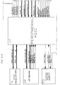
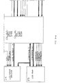
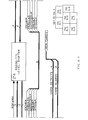
- FIG. 1 System diagram showing interconnections of the integrated circuit chips.
- Figure 4. A circuit board, front side.
- FIG. 1 Circuit board of Figure 4, rear side.
- Figures 6A, 6B Attachment of IC's to a circuit board.
- Figure 7 A test structure.
- FIGS 8A, 8B A computer reset structure.
- Figure 9 A border plate, display and keyboard.
- Fig. 1 shows a perspective view of the computer showing upper case 110b, lower case 110a, display 112, display frame 113, keyboard 118, key plate 118a, battery cover 123, hinge 111, latch 114, memory card tray 125, and display indicator graphics 130.
- Fig. 2 shows an exploded view of the computer keyboard 118 showing keyplate 118a with keys such as 181, 182, and 183, membrane 128 with cones such as 281, 282, and 283 each holding a conductive pad (not shown), and printed circuit board 138.
- Membrane 128 is elastomeric, and protrudes upward in a plurality of locations to form a plurality of elastomeric cones, one beneath each key, for example cones 281, 282, and 283 beneath keys 181, 182, and 183 respectively.
- Each cone is truncated at a flat (or relatively flat) upper surface which is contacted by an underside of its corresponding key. Extending downward from the flat upper surface of each of the elastomeric cones into the interior of the respective cone is an elastomeric conductive pill. When a key is pressed, its corresponding cone is compressed, moving its corresponding pill into position to span conductive traces (not shown) on the printed circuit board 138.
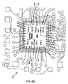
- Figure 4 shows a first side of the printed circuit board 138 including IC chip mounting areas 302, 304, 306.
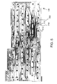
- Figure 5 shows the rear (i.e., second) side of the printed circuit board 138 including key contacts such as 310, 312, etc. to which conductive traces such as 318, 320, etc. are connected.
- Figure 6A shows in a side view how one IC chip 340 is electrically connected to printed circuit board 138 by bond wires 342, 344, etc. from pins 346, 348, etc. on chip 340 to bonding pads 350, 352 on printed circuit board 138.
- IC chips such as 340 thus preferably do not have the usual lead frame packaging.
- Figure 6B shows a top view of Figure 6A.
- Figure 7 shows a test structure as provided on printed circuit board 138.
- five separate test interconnect areas are provided, 360, 362, 364, 366, 368, each consisting of several pads such as 370, 372 to which test signals are provided by test cables such as 380.
- Test cable 380 is connected to printed circuit board 138 only when testing is to be performed.
- Card edge test connector 382 connects test cable 380 to the pads 370, 372, etc.
- indicating locator such as 390, 392 are provided as cut outs in the edge of printed circuit board 138 to locate the card edge test connectors such as 382. Note that as shown in Figures 4 and 5, such a test structure is provided on both sides of printed circuit board 138.
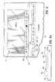
- Figure 8A shows a top view including dimensions of a portion of the keyboard 118 of the computer showing key 181 in keyplate 118a. Key 181 is partly cut away to expose cone 281.
- Figure 8B shows a cross-sectional view along line B-B in Figure 8A.
- a corresponding gap 400 has been left in keyplate 118a exposing cone 281.
- an object such as a pencil point
- this is done to reset the computer, by compressing conductive pill 402 against traces 404, 406 on printed circuit board 138.
- Fig. 3 shows a chip architecture computer system diagram showing interconnections of the integrated circuit chips physically shown in Fig. 4 plus the LCD driver chips located in the upper case and not shown in Fig. 4.
- the system of Fig. 3 includes an 80C88 microprocessor 16, a Peripheral ASIC chip 17, a System ASIC chip 18, and an LCD RAM 15, all physically located on a PCB board.
- This small combination of integrated circuit chips models in one embodiment an IBM XT computer. It may model other computers in other embodiments. They are physically located in the lower portion of the computer casing beneath the keyboard. Also physically located in the lower portion of the case is 512K of system RAM 19, a BIOS ROM chip 20, an application ROM chip 21, one or two memory cards 22a and 22b, and expansion port 23, and UART driver chip 24.
- VCO and other oscillators 11, and system power supply 13 (which in a preferred embodiment includes two AA batteries) are also located in the lower portion of the case in addition to keyboard 12.
- the LCD display Located in the upper portion of the case is the LCD display, an optional audio transducer, and a separate power supply.
- Display driver 14 includes row and column drivers and the analog power supply plus a unique display scan technique which lowers power. The entire system was designed to lower power. In particular, oscillators 11 require low power because they can be turned off when not actively used, a unique feature. The majority of the digital logic is CMOS, including memory 19, BIOS 20, application ROM 21. These draw microamps in the standby state and up to 100 milliamps in operation.
- VCO/OSCILLATORS This block contains all of the frequency oscillators used in the system. They include a display clock oscillator running at about 800 KHz, a communications clock oscillator running at 1.8432 MHz, a low frequency oscillator running at 32,768 Hz, and a voltage controlled oscillator (VCO) which operates between 1 and 8 MHz.
- VCO voltage controlled oscillator
- These three lines provide control signals from Peripheral ASIC 17 to block 11 to enable the respective oscillators. These signals are used to enable or disable the oscillators in block 11. There are only three enable signals because the low frequency oscillator is always running.
- KEYBOARD This is a standard matrix keyboard arranged in a 7x11 matrix of columns and rows. When a key is pressed, it completes the circuit between a selected row and column. The rows and columns are scanned by the keyboard control circuits within the Peripheral ASIC 17.
- a novel feature of Keyboard 12 is that fewer lines are needed between keyboard 12 and ASIC 17. Controller 17 uses only 7 return lines and 11 scan lines for a total of 18 lines to keyboard 12. Conventional keyboards use about 26 lines. Also unlike typical personal computers of today, no chip is dedicated as a keyboard controller. All keyboard control occurs in ASIC 17. Saving a chip saves power and board space.
- keyboard matrix 12 scan lines.
- the keyboard control circuits within the Peripheral ASIC 17 send out a scan signal on each of these lines individually and monitor the KBCOL[0..6] lines for a signal return.
- keyboard matrix 12 column lines These are the keyboard matrix 12 column lines. These lines are monitored during keyboard scanning for a signal which would indicate that a key is pressed providing a path from one of the KBSCAN[0..10] lines to one of the KBCOL[0..6] lines.
- this contact When this contact is connected by inserting a pointed object into the opening, it provides a path to ground causing a low signal on the line.
- This signal is monitored by the Peripheral ASIC 17 which resets the computer when a low transition is detected.
- SYSTEM POWER SUPPLY This is the power supply for the majority of the circuits within the computer.
- One notable exception is the display which has its own power supply located within block 14 as described above.
- This power supply includes the power source, namely two AA-size batteries, and necessary circuits to provide needed voltages and current for the computer.
- a low level output on this line forces the power supply into a low voltage mode.
- low voltage is three volts
- high voltage is five volts.
- automatic mode current demand is sensed, and when it passes a predetermined threshold, approximately 20 milliamperes in the current embodiment, it moves the voltage output from low to high voltage after a programmed delay.
- This signal is controlled by a bit within the Peripheral ASIC 17 allowing software to select between the high voltage and automatic modes of power supply operation.
- This signal from block 13 to the Peripheral ASIC is used to monitor the voltage of the system batteries. It is low to indicate that batteries are above a predetermined threshold (see discussion of BATMON), and goes high when these batteries fall below the threshold.
- This signal is monitored by the Peripheral ASIC 17 and may interact with software running on the processor 16. Since software running on the processor is able to monitor the real time condition of the batteries and determine when the batteries are about to expire, the BIOS will refuse to move from the off state when it is determined that doing so would jeopardize the integrity of the system memory and processor states.
- This signal is used by the battery voltage monitor circuits in 13.
- the signal can be manipulated by the processor 16 to set the threshold at which LOWBAT will change states.
- BATMON is high, the threshold is 1.8 volts.
- the threshold is 1.6 volts. This is used to sense low and dead battery conditions.
- This signal controls the LCD power supply within 14. When it is low, the power supply is enabled and running. When it is high, the power supply is disabled and producing no output. This signal is controlled by a bit within the Peripheral ASIC 17 which can be manipulated by the processor.
- VIDEO DISPLAY This block contains the LCD display driver circuits, the display power supply, the LCD screen, an audio transducer, and drive circuits for the audio transducer.
- LCD driver 14 and LCD RAM 15 control a liquid crystal display screen which is used in an embodiment of the present invention.
- LCD driver 14 is described in commonly assigned U.S. patent application serial no. 07/374,340 (US-A-5 130 703) invented by John P. Fairbanks, Andy C. Yuan, and Lance T. Klinger entitled "POWER SYSTEM AND SCAN METHOD FOR LIQUID CRYSTAL DISPLAY".
- LCD RAM 15 receives information about characters or graphic images to be displayed on the LCD screen.
- LCD RAM 15 includes a character memory which stores an ASCII representation and display attribute for each display character position, bit map images of each character in the character set currently in use, and a bit map memory where each display pixel on the LCD display is represented.
- a look-up table is also stored which is used by the display controller located within the Peripheral ASIC 17. Additional memory is provided which can be used as nonvolatile data storage.
- LCD RAM 15 includes two 32K x 8 static RAM chips. These chips store character and attribute data, LCD bit map data, character bit map data, and character translation data.
- This signal line from the display control circuits within Peripheral ASIC 17 is used to chip select one of the two RAM chips within LCD RAM 15. Specifically, this line selects the RAM used to store character, attribute, and LCD bit map data. This line is connected to the chip select pin on the RAM chips in LCD RAM 15.
- This signal line from the display control circuits within Peripheral ASIC 17 is used to enable the currently selected RAM chip within LCD RAM 15 (see discussion of VRAMCSN and VROMCSN) to drive data from the memory location specified by LCDADDR[0..14] onto the data bus LCDDATA[0..7].
- This signal line from the display control circuits within Peripheral ASIC 17 causes the currently selected RAM chip within LCD RAM 15 (see discussion of VRAMCSN and VROMCSN) to latch the data on LCDDATA[0..7] into the address specified by LCDADDR[0..14].
- This signal line from the display control circuits within Peripheral ASIC 17 is used to chip select one of the two RAM chips within LCD RAM 15. Specifically, this line selects the RAM used to store character bit maps and translation address data. It is connected to the chip select pin on the RAM chips within LCD RAM 15.
- 80C88 CPU This is the processor on which the architecture of the computer is based. It may be purchased from Intel Corporation, Harris Semiconductor, or OKI Semiconductor.
- processor status pins of microprocessor 16 are connected to the 8288 compatible Bus Controller cell located with the System ASIC 18. Their function is detailed in the data sheet of both the 80C88 and 8288 components available from Intel Corporation.
- This signal line is connected to the NMI (non maskable interrupt) pin of the processor 16.
- a signal on this line is generated by the System ASIC 18 and is the processor 16 non-maskable interrupt.
- the term nonmaskable interrupt indicates the interrupt cannot be masked by the microprocessor 16. This interrupt can be masked by circuits external to microprocessor 16.
- Processor 16 address data bus lines. These lines are the multiplexed address and data bus of the processor and connect to the peripheral ASIC 17 and the 8288 compatible Bus Controller cell located with the System ASIC 18. Their function is detailed in the data sheet of both the 80C88 and 8288 components available from Intel Corporation.
- the system clock signal is generated within the Peripheral ASIC 17 (where it is also used) and is derived either from the VCO oscillator located in block 11 or from an external source provided on line EXTSYSCLK.
- the signal on this line comes from the Peripheral ASIC 17. Circuits within the Peripheral ASIC 17, the System ASIC 18 (see SREADY), or external devices connected through the Expansion Port 23 (see IOCHRDY) may use this line to synchronize data transfer with the processor 16.
- PERIPHERAL ASIC 17 is the interface between the processor and peripheral devices, including keyboard 12, system power supply 13, LCD display driver 14, and LCD RAM 15. It also interfaces to oscillators 11 and turns them on and off under software control.
- the PERIPHERAL ASIC is designed to interface to a 11 row by 7 column matrix keyboard.
- the keyboard controller scans the keys by driving a single row low (to 0) and sampling the column inputs. If a key is down, the controller determines whether it is a new push or the key is just being held down. If it is a new push, the controller will generate the appropriate scan code and interrupt the processor via interrupt request, IRQ1. The controller will then suspend sampling until the interrupt is cleared by writing a one followed by a zero to bit 7 of port 0061h. Scan codes are read from port 0060h. Table 1 lists the scan code returned for each key in the 11 x 7 matrix. If no key is pushed the controller will continuously scan the keyboard until a key is detected.
- the controller will repeatedly interrupt the processor. Keyboard repeat times are broken into two classifications, the time before the first repeat interrupt, and the time for subsequent repeat interrupts. Repeat times may be programmed by writing to bits 4 - 7 of port F6E0h. Table 2 shows the corresponding repeat times for values written to port F6E0h.
- the keyboard controller runs off a 32.768 Khz clock, with each row being scanned approximately 256 times a second. Keyboard scanning may be halted by writing a one to bit 6 of port 0061h. Writing a zero back to bit 6 of port 0061h will resume scanning where the controller left off.
- the keyboard controller modifies the scan codes of certain keys depending upon the level of the PQKEYN input. This input, which is grounded when its corresponding key is pushed, will cause certain keys to return an alternate scan code. Table 1 lists the scan codes of those keys affected by the PQKEYN input. Table 2 lists keyboard repeat speeds.
- KEYBOARD SCAN CODES ROW # COL 0 COL 1 COL 2 COL 3 COL 4 COL 5 COL 6 ROW 0 KEY UP-ARW R-SH J ALT F : NULL NM CODE 48 36 24 38 21 27 00 PQ CODE 49 36 24 38 21 4E 00 ROW 1 KEY RTN SP DN-ARW L Z H INS NM CODE 1C 39 50 26 2C 23 52 PQ CODE 4C 39 51 26 2C 23 52 ROW 2 KEY D K G ' R-ARW DEL L-ARW NM CODE 20 25 22 28 4D 53 4B PQ CODE 20 25 22 28 4F 53 47 ROW 3 KEY CTL U P X B , NULL NM CODE 1D 16 19 2D 30 33 00 PQ CODE 1D 16 4A 2D 30 33 00 ROW 4 KEY O ] C N .
- the PERIPHERAL ASIC includes a MDA and CGA compatible display controller. It generates all needed signals, as well as refresh data to drive a 640 x 200 pixel LCD (liquid crystal display).
- the display controller in the PERIPHERAL ASIC may be disabled, allowing for an external controller by writing a one to bit 1 of port F6Elh.
- the PERIPHERAL ASIC's display controller is enabled upon reset.
- the PERIPHERAL ASIC's display controller may respond as either an MDA or a CGA video adapter. Writing a 0/1 to port F6E1 will select MDA/CGA compatibility. The display controller is in MDA mode upon reset.
- the PERIPHERAL ASIC includes many features for managing power consumption including the ability to power down and disable parts of the machine and stop clocks. Included is the ability to determine when to disable features. To do this, four special NMI's are generated. The first NMI interrupts the processor when timer interrupt requests, IRQ0, have occurred. This give the BIOS the capability of timing events even when the normal timer interrupt vector has been stolen. The second NMI is generated on keyboard interrupt requests, IRQ1. These are used to monitor keyboard input and to allow support for special function keys not supported in the hardware. The third NMI is an interrupt when memory address 00058h has been read. This is an indication that the INT16h software interrupt has been called. This is used to determine if the system is idle.
- the software may disable certain computer functions using special I/O ports, thus lowering power consumption.
- the final and most powerful NMI is the On/off key input. This comes from a key on the keyboard that notifies the BIOS that the user wishes to turn the system off. Lower power techniques using these features are disclosed in commonly assigned U.S. application serial no. 07/373,440, (US-A-5 428 790) invented by Leroy D. Harper, et al., entitled COMPUTER POWER MANAGEMENT SYSTEM, attorney docket no. M-924.
- the processor clock may be disabled with a write to port F6ECh bit 6 with a zero followed by a one.
- the clock will stop low in the middle of the last I/O write cycle and remain low until an interrupt wakes it.
- An IRQO, IRQ1, IRQ4, or NMI may wake the system, if enabled.
- Each NMI has a mask bit in a special register and the IRQ's have a separate clock mask bit that will mask it from waking the processor, but not mask the interrupt request line from becoming active.
- the UART clock may be stopped by writing a one to bit 7 of port F6ECh.
- the charge pump on the RS-232 compatible drivers may be disabled by writing a one to bit 5 of port F6ECh.
- the LCD display can be turned off by writing a one to bit 3 of port F6ECh. This also stops the display clock, refreshing, contrast and all associated signals. Finally, the power supply voltage may be set to 5 Volts with a write of a zero to bit 2 of port F6ECh. This output will go to high impedance with a write of a one to bit 4 of port F6ECh forcing the power supply into automatic mode. In this mode, the power supply voltage will be set based on current consumption.
- the computer also includes a second set of symbols such as 516, 518, 520, 524 as shown in Figure 9 imprinted on a margin of the keyboard 118.
- These symbols such as 516, 518, 520, 524 describe the functions of an adjacent row of keyboard function keys (not shown). In one embodiment, four symbols in four different colors are provided adjacent each function key. Keys for "shift”, “alt”, “ctrl”, and a special logo key (not shown) are correspondingly colored to indicate that simultaneously pressing the "shift”, “alt”, “ctrl", or the special logo key with the adjacent function key produces the functions noted in color by the symbol 502, 504, etc., adjacent to the function key.
Landscapes
- Engineering & Computer Science (AREA)
- Theoretical Computer Science (AREA)
- Physics & Mathematics (AREA)
- General Engineering & Computer Science (AREA)
- General Physics & Mathematics (AREA)
- Computing Systems (AREA)
- Computer Hardware Design (AREA)
- Power Sources (AREA)
- Investigating, Analyzing Materials By Fluorescence Or Luminescence (AREA)
- Charge And Discharge Circuits For Batteries Or The Like (AREA)
Description
- This invention relates to a compact portable computer including a keyboard, in particular a battery operated computer using a liquid crystal display.
- Personal computers have become faster and smaller in recent years. Desk top computers typically use household power and run commercially available software written for execution through an operating system such as MS-DOS® (MS-DOS® is a registered trademark of Microsoft Corporation) or Unix® (Unix® is a registered trademark of American Telephone & Telegraph). In addition to the computing unit, these computers include a monitor for displaying information to the user and a keyboard for receiving information from the user. They may include disk drives, a printer, a communication modem, and may include even more peripheral devices. Since the computer must be compatible with commercially available software, a basic input/output system (BIOS) which is unique for each computer converts commands generated by the operating system or application program to specific machine commands implemented by the hardware of the machine. These computers include an internal clock which operates continuously when the machine is turned on and controls the central processor to access memory, load registers, read and write to disk, detect keyboard use, and control a display, all operations synchronized with cycles of the internal clock. In addition, if the computer accesses an external port, the external communications may be controlled by an asynchronous clock through a UART (universal asynchronous receiver/transmitter). The power used by these desk-top wall-plug computers has not been of particular concern because it is small when compared with power used by other appliances which also use the same power source.
- Methods for reducing power used by a computer have included using CMOS circuitry, and using liquid crystal display monitors rather than cathode ray tube monitors or plasma display technology.
- There exists a class of small, lightweight computers which have been designed for low power and may use batteries. These computers do not have the computing capability of a desk top machine nor the ability to run the full range of commercial software and operating systems available for desk top machines. They typically have reduced display resolution and inconvenient keyboards.
- Another class of computers generally described as lap top computers are battery operated, portable, and may run a broad range of commercial software. However, these lap top computers are powered by bulky rechargeable batteries and can only operate for a few hours before requiring the batteries to be recharged.
- The present invention provides a compact portable computer as defined in claim 1.
- In a preferred embodiment the computer is housed in a two-part low profile rectangular case hinged along one long edge and latched at an opposite edge. The hinge extends along a back edge of the case and rotatably joins upper and lower portions of the case. This hinge is described in commonly assigned U.S. application serial no. 07/373,769 (US-A-4 984 706) invented by Noah L. Anglin entitled "HINGE FOR HAND HELD COMPUTER".
The case is preferably of a plastic such as polycarbonate and/or ABS plastic or both. The case is of molded construction. - A lower portion of the case includes a keyboard, one or two memory cards, batteries, and most of the integrated circuit components of the computer. The integrated circuit components in this lower portion are attached to the lower side of a printed circuit board which occupies most of the rectangular area encompassed by the case. Included in these integrated circuit components are two ASIC (application specific integrated circuit) chips. In order to conserve space, particularly vertical space, these ASIC chips are put on the board without the usual packaging. Such packaging (which is omitted) would include a plastic or ceramic protective cover surrounding a lead frame which connects interior pin-outs to exterior pins. The unpackaged chip is bonded directly to the lower printed circuit board, thereby saving both horizontal and vertical space in the present very compact structure. The microprocessor chip is also attached directly to the printed circuit board without intervening packaging, which reduces connection points and cost.
- Also attached to the lower side of this printed circuit board are connectors for receiving removable memory cards, preferably at least two connectors for two cards. These connectors are the same thickness as the card itself. No circuit components are located on that part of the printed circuit board adjacent to where the memory cards are placed, so that the memory cards fit within the existing envelope of the computer housing. A tray for holding a memory card which forms part of the lower case is described in detail in commonly assigned U.S. application serial no. 07/374,409 (US-A-5 315 478) invented by Noah L. Anglin and Peter F. Cadwell entitled "MEMORY CARD TRAY FOR PORTABLE COMPUTER".
- At one or several edges of the printed circuit board are pads to which traces extend from pins of the integrated circuit chips to which test signals are applied during manufacturing. These pads are accessed with edge connectors which are designed to slip over an edge of the board and make electrical contact with the pads. This avoids the need for applying test probes to the interior of the circuit board and thereby saves time and avoids testing mistakes.
- The upper side of the same printed circuit board in the lower portion of the case serves as a back plate for the keyboard. Traces for electrically detecting each key state are applied directly to the upper side of this printed circuit board. The keyboard includes a keyplate through which extend a plurality of keys. The keys press corresponding cones in an insulating flexible membrane, each cone including a conductive flexible pad which in a compressed position spans conductive traces on the printed circuit board and in a non-compressed position leaves these conductive traces unconnected.
- The keyboard occupies most of the inner surface of the lower case, occupying more than half, and preferably 70% or more of the surface area of the inner surface of the lower case.
- The upper side of this printed circuit board also includes traces for detecting a machine reset. As a novel feature of an embodiment of the present invention, reset is activated by inserting a pointed object such as a pencil point through an opening in the keyboard and pressing an electrically conductive pad rather than by pressing a key or combination of keys.
- As another novel feature of an embodiment of the present invention, one of the keyboard keys is an on/off toggle key. The computer never turns completely off, but in the off state operates only a low frequency clock which keeps time-of-day.
- After testing of the lower printed circuit board and installation of the membrane during assembly of the computer, the keyplate which holds the keys in position is welded to the lower portion of the case in order to achieve accurate registration of the keys, the membrane, and the traces.
- Located between the hinge and the keyboard area is a compartment including batteries and a capacitor. This capacitor is sufficient to maintain volatile memory with the computer in the off state while batteries are being changed. The batteries are covered by a plate which is imprinted with descriptions of a top row of keyboard function keys, these function keys being located just adjacent to the battery cover plate. In one embodiment, four notations in four different colors are imprinted on the cover plate adjacent each function key. Keys for "shift", "alt", "ctrl", and a special logo key are correspondingly colored to indicate to a user that combining the "shift", "alt", "ctrl", or the logo key with the adjacent function key produces the function noted in color adjacent the function key. Alternate cover plates, tapes for attaching to the cover plate, or cards for placing adjacent this cover plate may be provided for use with different software packages.
- An upper portion of the case houses a liquid crystal display plus a separate power supply for the liquid crystal display. In one embodiment a space is provided between the display and the outside of the upper case for insertion of a display back light powered by separate batteries or other power source. This back light is described in detail in commonly assigned U.S. application serial no. 07/276,167 (US-A-5 030 943).
- The power supply for the liquid crystal display is described in detail in commonly assigned U.S. application serial no. 07/374,340 (US-A-5 130 703) invented by John. P. Fairbanks, Andy. C. Yuan, and Lance T. Klinger, entitled "POWER SYSTEM AND SCAN TECHNIQUE FOR A LIQUID CRYSTAL DISPLAY", attorney docket no. M-806.
- The liquid crystal display occupies most of the entire area enclosed by the upper portion of the case, with a narrow frame surrounding the liquid crystal display and its cover.
- The display when displaying characters shows 25 lines of 80 characters per line. A line of characters is typically 8 pixels tall so that the standard 25 lines of text are displayed using 200 rows of pixels.
Additionally, a status line using one or more rows of pixels at the top, bottom or both, of the display are provided for showing status of various software programs and hardware conditions. Coordinating with these displayed status lines are imprinted legends along the top, bottom, or both margins of the display frame for indicating to the user the meanings represented by these status lines. As with the keyboard, different legends can be provided for different software packages. - The supporting mechanism for the liquid crystal display is described in commonly assigned U.S. application serial no. 07/359,191 (US-A-5 002 368) invented by Noah L. Anglin, and entitled "LIQUID CRYSTAL DISPLAY MOUNTING STRUCTURE".
- Since separate power supplies are located in the two portions of the computer case, the number of current carrying lines which must extend between the upper and lower housing is minimized. A cable including these lines extends from the lower to the upper portion of the case and is located toward the interior of the computer from the hinge axis. The cable has sufficient length to span from its lower point of connection to its upper point of connection when the computer case is fully open. The spiral design of the cable acts as a spring so that when the computer is closed, the excess cable slack is taken up in a cable cover located in the upper or lower portion of the case, preferably lower. This cable cover protects the cable from excess flexure, assuring long life.
- This arrangement of the components allows for the computer to fold to a very compact size for being carried and to open to a convenient size in which the two components which interface with the user, namely the keyboard and the display, are large enough to be convenient. To further reduce thickness, the keys are made so that some keys are pressed by the display upon closing the computer case. Preferably, these are the front (lower) row of keys.
- In one embodiment, the keyboard is controlled such that a multiplicity of key presses does not cause an executing program to cease operation. The on/off key is a key not depressed when the case is closed. When the on/off key is pressed to toggle the computer to its off state, other keys are deactivated such that pressing the other keys upon closing the case is not detected by the computer. When the computer is in this off state, the processor does not lose its place in the program which was running. All memory remains static but execution is halted until the machine is moved out of the off state. While in this off state, timer interrupts are processed allowing time of day updating, and allowing software which uses the time of day interrupt to process the interrupt.
- An embodiment of the present invention includes a power management system which maintains as many components of the computer in an off state for as much time as possible even when the computer is on. Individual components can be turned off while other components remain on. Components of the machine which can be turned off while the machine appears to a user to be on include the oscillator and clock which cycle the central processor, another oscillator and clock which control the display, a direct memory access (DMA) clock tied to the central processor oscillator which controls direct memory access circuits, and an oscillator and clock for communication to an external port. While the machine is turned on, that is, while the display is on and the machine is responding to user input, the hardware detects activities for which some parts of the machine can be turned off. These clocks can actually be turned off while the user is in the midst of executing a program. For example, when a user is executing a word processing program, the clock which controls the central processor is turned off for most of the time between one keystroke and the next.
- In a preferred embodiment, four activities are monitored for determining when parts of the machine can be turned off: the state of the on/off switch, keyboard presses, software activity and clock ticks generated by a low frequency clock and a divider circuit. When these activities are not occurring, certain clocks and devices driven by the clocks are turned off. Because in a preferred embodiment CMOS circuitry is used, which uses most of its power when switching, turning off oscillators and their associated clocks greatly reduces power consumption of the system. Turning off devices themselves also reduces power. This power management system is described in detail in commonly assigned U.S. application serial no. 07/373,440 (US-A-5 428 790) invented by Leroy D. Harper, Grayson C. Schlichting, Douglas A. Hooks, Ian H.S. Cullimore, and Gavin Bradshaw, attorney docket no. M-924, entitled "POWER MANAGEMENT SYSTEM FOR LOW POWER COMPUTER".
- US-A-4 571 456 discloses a portable computer of conventional construction with a main printed circuit board, carrying most of the integrated circuit devices of the computer, located in the base section of the computer housing and a conventional keyboard located on the upper surface of the base section.
- US-A-4 328 399 discloses a pushbutton switch assembly for a telecommunications apparatus. In one embodiment of this pushbutton assembly, circuit components such as integrated circuits are mounted on one side of a steel ceramic circuit board, whereas the other side of the board includes switch contacts for detecting key presses of keys located on the other side of the board.
- CAMBRIDGE COMPUTER LTD. "Z88 Cambridge Computer User Guide" 1987, pages 8 and 9 and M&P Computer 1988, pages 90 - 93, "Marco Micheletti: Cambridge Z88 - Eureka! I1 Portatile disclose portable computers. These computers have a reset function which is not activated with a normal key but by means of an object (pin or paperclip) inserted through a hole in the case of the computer to reach and activate the reset.
- Figure 1. Perspective view of the computer.
- Figure 2. Exploded view of keyboard.
- Figure 3. System diagram showing interconnections of the integrated circuit chips.
- Figure 4. A circuit board, front side.
- Figure 5. Circuit board of Figure 4, rear side.
- Figures 6A, 6B. Attachment of IC's to a circuit board.
- Figure 7. A test structure.
- Figures 8A, 8B. A computer reset structure.
- Figure 9. A border plate, display and keyboard.
- Identical reference numbers in various figures refer to identical or similar structures.
- Fig. 1 shows a perspective view of the computer showing upper case 110b, lower case 110a, display 112, display frame 113, keyboard 118, key plate 118a, battery cover 123, hinge 111, latch 114, memory card tray 125, and display indicator graphics 130.
- Fig. 2 shows an exploded view of the computer keyboard 118 showing keyplate 118a with keys such as 181, 182, and 183, membrane 128 with cones such as 281, 282, and 283 each holding a conductive pad (not shown), and printed circuit board 138.
- Membrane 128 is elastomeric, and protrudes upward in a plurality of locations to form a plurality of elastomeric cones, one beneath each key, for example cones 281, 282, and 283 beneath keys 181, 182, and 183 respectively. Each cone is truncated at a flat (or relatively flat) upper surface which is contacted by an underside of its corresponding key. Extending downward from the flat upper surface of each of the elastomeric cones into the interior of the respective cone is an elastomeric conductive pill. When a key is pressed, its corresponding cone is compressed, moving its corresponding pill into position to span conductive traces (not shown) on the printed circuit board 138.
- Figure 4 shows a first side of the printed circuit board 138 including IC chip mounting areas 302, 304, 306.
- Figure 5 shows the rear (i.e., second) side of the printed circuit board 138 including key contacts such as 310, 312, etc. to which conductive traces such as 318, 320, etc. are connected.
- Figure 6A shows in a side view how one IC chip 340 is electrically connected to printed circuit board 138 by bond wires 342, 344, etc. from pins 346, 348, etc. on chip 340 to bonding pads 350, 352 on printed circuit board 138. IC chips such as 340 thus preferably do not have the usual lead frame packaging. Figure 6B shows a top view of Figure 6A.
- Figure 7 shows a test structure as provided on printed circuit board 138. As shown, five separate test interconnect areas are provided, 360, 362, 364, 366, 368, each consisting of several pads such as 370, 372 to which test signals are provided by test cables such as 380. Test cable 380 is connected to printed circuit board 138 only when testing is to be performed. Card edge test connector 382 connects test cable 380 to the pads 370, 372, etc. As shown, indicating locator such as 390, 392 are provided as cut outs in the edge of printed circuit board 138 to locate the card edge test connectors such as 382. Note that as shown in Figures 4 and 5, such a test structure is provided on both sides of printed circuit board 138.
- Figure 8A shows a top view including dimensions of a portion of the keyboard 118 of the computer showing key 181 in keyplate 118a. Key 181 is partly cut away to expose cone 281.
- Figure 8B shows a cross-sectional view along line B-B in Figure 8A. As shown in Figure 8B (key 181 not shown) a corresponding gap 400 has been left in keyplate 118a exposing cone 281. Thus it is possible to press down on cone 281 with an object (such as a pencil point) through gap 400. Preferably this is done to reset the computer, by compressing conductive pill 402 against traces 404, 406 on printed circuit board 138.
- Fig. 3 shows a chip architecture computer system diagram showing interconnections of the integrated circuit chips physically shown in Fig. 4 plus the LCD driver chips located in the upper case and not shown in Fig. 4.
- The system of Fig. 3 includes an 80C88 microprocessor 16, a Peripheral ASIC chip 17, a System ASIC chip 18, and an LCD RAM 15, all physically located on a PCB board. This small combination of integrated circuit chips models in one embodiment an IBM XT computer. It may model other computers in other embodiments. They are physically located in the lower portion of the computer casing beneath the keyboard. Also physically located in the lower portion of the case is 512K of system RAM 19, a BIOS ROM chip 20, an application ROM chip 21, one or two memory cards 22a and 22b, and expansion port 23, and UART driver chip 24. VCO and other oscillators 11, and system power supply 13 (which in a preferred embodiment includes two AA batteries) are also located in the lower portion of the case in addition to keyboard 12.
- Located in the upper portion of the case is the LCD display, an optional audio transducer, and a separate power supply.
- Display driver 14 includes row and column drivers and the analog power supply plus a unique display scan technique which lowers power. The entire system was designed to lower power. In particular, oscillators 11 require low power because they can be turned off when not actively used, a unique feature. The majority of the digital logic is CMOS, including memory 19, BIOS 20, application ROM 21. These draw microamps in the standby state and up to 100 milliamps in operation.
- On the reverse side of the PC board is the lower level of the keyboard unit. The contact lines of the keyboard are applied directly to the reverse side of the PC board.
- Following is a list of the blocks and lines shown in Fig. 3.
- VCO/OSCILLATORS. This block contains all of the frequency oscillators used in the system. They include a display clock oscillator running at about 800 KHz, a communications clock oscillator running at 1.8432 MHz, a low frequency oscillator running at 32,768 Hz, and a voltage controlled oscillator (VCO) which operates between 1 and 8 MHz.
- There are four oscillators. The oscillator which drives the Processor 16 is voltage controlled, so if there is a sag in the supplied voltage, the frequency will drop to compensate for the lower performance of the CMOS circuits. This also allows the processor speed to be automatically adjusted when the system power supply changes output voltages. At 5 volts all components will run at 8 MHz. At 3 volts they would not run at 8 MHz but at 2 MHz the system will run. There is a power advantage to running at 3 volts because
- In a preferred embodiment there are actually two modes, 5 volts and automatic. In automatic mode, the system moves after a delay from 3 volts to 5 volts when power demand is heavier. When current exceeds a certain level, preferably between 1 and 10 milliamps, the system moves to 5 volts. The novel system for moving between two voltage levels is described in detail in commonly assigned U.S. application serial no. 07/374,514 (US-A-5 021 679) invented by John P. Fairbanks and Andy C. Yuan, entitled "VOLTAGE MANAGEMENT SYSTEMS FOR MULTIPLE VOLTAGE POWER SUPPLY".
- These four lines provide the oscillator outputs from block 11 to the Peripheral ASIC 17 for distribution to other parts of the system.
- These three lines provide control signals from Peripheral ASIC 17 to block 11 to enable the respective oscillators. These signals are used to enable or disable the oscillators in block 11. There are only three enable signals because the low frequency oscillator is always running.
- KEYBOARD. This is a standard matrix keyboard arranged in a 7x11 matrix of columns and rows. When a key is pressed, it completes the circuit between a selected row and column. The rows and columns are scanned by the keyboard control circuits within the Peripheral ASIC 17.
- A novel feature of Keyboard 12 is that fewer lines are needed between keyboard 12 and ASIC 17. Controller 17 uses only 7 return lines and 11 scan lines for a total of 18 lines to keyboard 12. Conventional keyboards use about 26 lines. Also unlike typical personal computers of today, no chip is dedicated as a keyboard controller. All keyboard control occurs in ASIC 17. Saving a chip saves power and board space.
- These are the keyboard matrix 12 scan lines. The keyboard control circuits within the Peripheral ASIC 17 send out a scan signal on each of these lines individually and monitor the KBCOL[0..6] lines for a signal return.
- These are the keyboard matrix 12 column lines. These lines are monitored during keyboard scanning for a signal which would indicate that a key is pressed providing a path from one of the KBSCAN[0..10] lines to one of the KBCOL[0..6] lines.
- This is a line from the keyboard 12 which is associated with specially labeled key. When this key is pressed, it provides a path to ground causing a low signal on this line. When said key is not pressed there is no path to ground. The line is pulled up to VDD to assure that its default state is high. This signal is monitored by the Peripheral ASIC 17 and may interact with software running on the processor 16.
- This is a line from keyboard 12 which is associated with a special key used to turn the computer on and off. When this key is pressed, it provides a path to ground causing a low signal on this line. Otherwise the line is pulled up to VDD to assure that its default state is high. This signal is monitored by the Peripheral ASIC 17 and may interact with software running on the processor 16.
- This is a line from the keyboard 12 which is associated with the reset opening in the keyboard. When this contact is connected by inserting a pointed object into the opening, it provides a path to ground causing a low signal on the line. This signal is monitored by the Peripheral ASIC 17 which resets the computer when a low transition is detected.
- SYSTEM POWER SUPPLY. This is the power supply for the majority of the circuits within the computer. One notable exception is the display which has its own power supply located within block 14 as described above. This power supply includes the power source, namely two AA-size batteries, and necessary circuits to provide needed voltages and current for the computer.
- This signal into block 13 is used to select from two possible supply modes: high voltage output (SELVDD= Low), and automatic mode (SELVDD=Tristate). In another embodiment a low level output on this line forces the power supply into a low voltage mode. In the current embodiment, low voltage is three volts, and high voltage is five volts. In automatic mode, current demand is sensed, and when it passes a predetermined threshold, approximately 20 milliamperes in the current embodiment, it moves the voltage output from low to high voltage after a programmed delay. This signal is controlled by a bit within the Peripheral ASIC 17 allowing software to select between the high voltage and automatic modes of power supply operation.
- This signal from block 13 to the Peripheral ASIC is used to monitor the voltage of the system batteries. It is low to indicate that batteries are above a predetermined threshold (see discussion of BATMON), and goes high when these batteries fall below the threshold. This signal is monitored by the Peripheral ASIC 17 and may interact with software running on the processor 16. Since software running on the processor is able to monitor the real time condition of the batteries and determine when the batteries are about to expire, the BIOS will refuse to move from the off state when it is determined that doing so would jeopardize the integrity of the system memory and processor states.
- This signal is used by the battery voltage monitor circuits in 13. The signal can be manipulated by the processor 16 to set the threshold at which LOWBAT will change states. When BATMON is high, the threshold is 1.8 volts. When it is low, the threshold is 1.6 volts. This is used to sense low and dead battery conditions.
- This is the battery voltage from the computer batteries which is used by the circuits and power supply within block 14 and ranges between 1.6 and 1.3 volts.
- This is the signal from Peripheral ASIC 17 to the drive circuits of the audio transducer within 14. This signal is controlled by a bit within the Peripheral ASIC 17 which can be manipulated by the processor.
- This signal controls the LCD power supply within 14. When it is low, the power supply is enabled and running. When it is high, the power supply is disabled and producing no output. This signal is controlled by a bit within the Peripheral ASIC 17 which can be manipulated by the processor.
- These five signals are used to clock the LCD driver chips within 14. They are generated by the display drive refresh circuits within the Peripheral ASIC 17.
- VIDEO DISPLAY. This block contains the LCD display driver circuits, the display power supply, the LCD screen, an audio transducer, and drive circuits for the audio transducer.
- LCD driver 14 and LCD RAM 15 control a liquid crystal display screen which is used in an embodiment of the present invention. LCD driver 14 is described in commonly assigned U.S. patent application serial no. 07/374,340 (US-A-5 130 703) invented by John P. Fairbanks, Andy C. Yuan, and Lance T. Klinger entitled "POWER SYSTEM AND SCAN METHOD FOR LIQUID CRYSTAL DISPLAY".
- THE LCD RAM 15 is described in commonly assigned U.S. patent application serial no. 07/374,884 (WO91/00587) invented by Leroy D. Harper, John W. Corbett, Douglas A. Hooks, Grayson C. Schlichting, Renee D. Bader, and John P. Fairbanks entitled "VIDEO IMAGE CONTROLLER FOR LOWER POWER COMPUTER". LCD RAM 15 receives information about characters or graphic images to be displayed on the LCD screen. LCD RAM 15 includes a character memory which stores an ASCII representation and display attribute for each display character position, bit map images of each character in the character set currently in use, and a bit map memory where each display pixel on the LCD display is represented. A look-up table is also stored which is used by the display controller located within the Peripheral ASIC 17. Additional memory is provided which can be used as nonvolatile data storage. LCD RAM 15 includes two 32K x 8 static RAM chips. These chips store character and attribute data, LCD bit map data, character bit map data, and character translation data.
- These are the data lines between the display controller within the Peripheral ASIC 17 and both the LCD RAM 15 and the LCD driver chips located within display driver 14. Data is sent from Peripheral ASIC 17 to display driver 14 during display refresh cycles in order to update data in the driver chips which is ultimately displayed on the LCD display. A two way path exists between Peripheral ASIC 17 and LCD RAM 15 and is used when the display driver circuits in Peripheral ASIC 17 read and write data in the two RAM chips 15.
- These are the address lines used to access the two RAM chips in LCD RAM 15. The addresses are generated by display control circuits within Peripheral ASIC 17.
- This signal line from the display control circuits within Peripheral ASIC 17 is used to chip select one of the two RAM chips within LCD RAM 15. Specifically, this line selects the RAM used to store character, attribute, and LCD bit map data. This line is connected to the chip select pin on the RAM chips in LCD RAM 15.
- This signal line from the display control circuits within Peripheral ASIC 17 is used to enable the currently selected RAM chip within LCD RAM 15 (see discussion of VRAMCSN and VROMCSN) to drive data from the memory location specified by LCDADDR[0..14] onto the data bus LCDDATA[0..7].
- This signal line from the display control circuits within Peripheral ASIC 17 causes the currently selected RAM chip within LCD RAM 15 (see discussion of VRAMCSN and VROMCSN) to latch the data on LCDDATA[0..7] into the address specified by LCDADDR[0..14].
- This signal line from the display control circuits within Peripheral ASIC 17 is used to chip select one of the two RAM chips within LCD RAM 15. Specifically, this line selects the RAM used to store character bit maps and translation address data. It is connected to the chip select pin on the RAM chips within LCD RAM 15.
- 80C88 CPU. This is the processor on which the architecture of the computer is based. It may be purchased from Intel Corporation, Harris Semiconductor, or OKI Semiconductor.
- These are processor status pins of microprocessor 16 and are connected to the 8288 compatible Bus Controller cell located with the System ASIC 18. Their function is detailed in the data sheet of both the 80C88 and 8288 components available from Intel Corporation.
- This is the processor pin LOCK from processor 16 and is connected to the System ASIC 18.
- This is the processor pin INTR which is used to generate interrupts. It is connected to the 8259 compatible Programmable Interrupt Controller cell located within the System ASIC 18. The function of this signal is detailed in the data sheet of both the 80C88 and 8259 components available from Intel Corporation.
- This signal line is connected to the NMI (non maskable interrupt) pin of the processor 16. A signal on this line is generated by the System ASIC 18 and is the processor 16 non-maskable interrupt. The term nonmaskable interrupt indicates the interrupt cannot be masked by the microprocessor 16. This interrupt can be masked by circuits external to microprocessor 16.
- Processor 16 address data bus lines. These lines are the multiplexed address and data bus of the processor and connect to the peripheral ASIC 17 and the 8288 compatible Bus Controller cell located with the System ASIC 18. Their function is detailed in the data sheet of both the 80C88 and 8288 components available from Intel Corporation.
- These are the high order processor 16 address lines. They are connected to both the circuits within the Peripheral ASIC 17, and the 8288 compatible Bus Controller cell located within the System ASIC 18. Their function is detailed in the data sheet of both the 80C88 and 8288 components available from Intel Corporation.
- This is the system clock signal line used to clock both the processor 16 and circuits within the System ASIC 18. The system clock signal is generated within the Peripheral ASIC 17 (where it is also used) and is derived either from the VCO oscillator located in block 11 or from an external source provided on line EXTSYSCLK.
- This is the READY signal line on the processor 16 and is used to extend processor 16 read and write operations to allow slower devices to interface with the processor 16. The signal on this line comes from the Peripheral ASIC 17. Circuits within the Peripheral ASIC 17, the System ASIC 18 (see SREADY), or external devices connected through the Expansion Port 23 (see IOCHRDY) may use this line to synchronize data transfer with the processor 16.
- This is one of two ASIC chips preferably used in an embodiment of the present invention. PERIPHERAL ASIC 17 is the interface between the processor and peripheral devices, including keyboard 12, system power supply 13, LCD display driver 14, and LCD RAM 15. It also interfaces to oscillators 11 and turns them on and off under software control.
- The PERIPHERAL ASIC is designed to interface to a 11 row by 7 column matrix keyboard. The keyboard controller scans the keys by driving a single row low (to 0) and sampling the column inputs. If a key is down, the controller determines whether it is a new push or the key is just being held down. If it is a new push, the controller will generate the appropriate scan code and interrupt the processor via interrupt request, IRQ1. The controller will then suspend sampling until the interrupt is cleared by writing a one followed by a zero to bit 7 of port 0061h. Scan codes are read from port 0060h. Table 1 lists the scan code returned for each key in the 11 x 7 matrix. If no key is pushed the controller will continuously scan the keyboard until a key is detected. If the last key pushed is held for a sufficient amount of time, the controller will repeatedly interrupt the processor. Keyboard repeat times are broken into two classifications, the time before the first repeat interrupt, and the time for subsequent repeat interrupts. Repeat times may be programmed by writing to bits 4 - 7 of port F6E0h. Table 2 shows the corresponding repeat times for values written to port F6E0h.
- The keyboard controller runs off a 32.768 Khz clock, with each row being scanned approximately 256 times a second. Keyboard scanning may be halted by writing a one to bit 6 of port 0061h. Writing a zero back to bit 6 of port 0061h will resume scanning where the controller left off.
- The keyboard controller modifies the scan codes of certain keys depending upon the level of the PQKEYN input. This input, which is grounded when its corresponding key is pushed, will cause certain keys to return an alternate scan code. Table 1 lists the scan codes of those keys affected by the PQKEYN input. Table 2 lists keyboard repeat speeds.
KEYBOARD SCAN CODES (HEX) ROW # COL 0 COL 1 COL 2 COL 3 COL 4 COL 5 COL 6 ROW 0 KEY UP-ARW R-SH J ALT F : NULL NM CODE 48 36 24 38 21 27 00 PQ CODE 49 36 24 38 21 4E 00 ROW 1 KEY RTN SP DN-ARW L Z H INS NM CODE 1C 39 50 26 2C 23 52 PQ CODE 4C 39 51 26 2C 23 52 ROW 2 KEY D K G ' R-ARW DEL L-ARW NM CODE 20 25 22 28 4D 53 4B PQ CODE 20 25 22 28 4F 53 47 ROW 3 KEY CTL U P X B , NULL NM CODE 1D 16 19 2D 30 33 00 PQ CODE 1D 16 4A 2D 30 33 00 ROW 4 KEY O ] C N . CAP A NM CODE 18 1B 2E 31 34 3A 1E PQ CODE 18 1B 2E 31 34 3A 1E ROW 5 KEY [ S L-SH V M I / NM CODE 1A 1F 2A 2F 32 17 35 PQ CODE 1A 1F 2A 2F 32 17 35 ROW 6 KEY F2 F5 F8 \ E TAB Y NM CODE 3C 3F 42 2B 12 0F 15 PQ CODE 3C 3F 42 2B 12 0F 15 ROW 7 KEY F10 F1 SCR F4 Q F7 R NM CODE 44 3B 46 3E 10 41 13 PQ CODE 45 3B 46 3E 10 41 13 ROW 8 KEY 1 3 7 9 - 5 = NM CODE 02 04 08 0A 0C 06 0D PQ CODE 02 04 08 0A 0C 06 0D ROW 9 KEY 4 ' 2 6 8 BK-SP 0 NM CODE 05 29 03 07 09 0E 0B PQ CODE 05 29 03 07 09 0E 0B ROW 10 KEY ESC T F3 W F6 PSCR F9 NM CODE 01 14 3D 11 40 37 43 PQ CODE 01 14 3D 11 40 37 43 KEYBOARD REPEAT SPEEDS PORT BITS VALUE DESCRIPTION F6E0 4-5 0 Initial repeat time of 625 ms. 4-5 1 Initial repeat time of 375 ms. 4-5 2 Initial repeat time of 281 ms. 4-5 3 Initial repeat time of 187 ms. 6-7 0 Subsequent repeat interval of 281 ms. 6-7 1 Subsequent repeat interval of 187 ms. 6-7 2 Subsequent repeat interval of 94 ms. 6-7 3 Subsequent repeat interval of 47 ms. - The PERIPHERAL ASIC includes a MDA and CGA compatible display controller. It generates all needed signals, as well as refresh data to drive a 640 x 200 pixel LCD (liquid crystal display). The display controller in the PERIPHERAL ASIC may be disabled, allowing for an external controller by writing a one to bit 1 of port F6Elh. The PERIPHERAL ASIC's display controller is enabled upon reset.
- The PERIPHERAL ASIC's display controller may respond as either an MDA or a CGA video adapter. Writing a 0/1 to port F6E1 will select MDA/CGA compatibility. The display controller is in MDA mode upon reset.
- The PERIPHERAL ASIC includes many features for managing power consumption including the ability to power down and disable parts of the machine and stop clocks. Included is the ability to determine when to disable features. To do this, four special NMI's are generated. The first NMI interrupts the processor when timer interrupt requests, IRQ0, have occurred. This give the BIOS the capability of timing events even when the normal timer interrupt vector has been stolen. The second NMI is generated on keyboard interrupt requests, IRQ1. These are used to monitor keyboard input and to allow support for special function keys not supported in the hardware. The third NMI is an interrupt when memory address 00058h has been read. This is an indication that the INT16h software interrupt has been called. This is used to determine if the system is idle. Once the software has determined that the machine is idle, it may disable certain computer functions using special I/O ports, thus lowering power consumption. The final and most powerful NMI is the On/off key input. This comes from a key on the keyboard that notifies the BIOS that the user wishes to turn the system off. Lower power techniques using these features are disclosed in commonly assigned U.S. application serial no. 07/373,440, (US-A-5 428 790) invented by Leroy D. Harper, et al., entitled COMPUTER POWER MANAGEMENT SYSTEM, attorney docket no. M-924.
- The processor clock may be disabled with a write to port F6ECh bit 6 with a zero followed by a one. The clock will stop low in the middle of the last I/O write cycle and remain low until an interrupt wakes it. An IRQO, IRQ1, IRQ4, or NMI may wake the system, if enabled. Each NMI has a mask bit in a special register and the IRQ's have a separate clock mask bit that will mask it from waking the processor, but not mask the interrupt request line from becoming active. The UART clock may be stopped by writing a one to bit 7 of port F6ECh. The charge pump on the RS-232 compatible drivers may be disabled by writing a one to bit 5 of port F6ECh. The LCD display can be turned off by writing a one to bit 3 of port F6ECh. This also stops the display clock, refreshing, contrast and all associated signals. Finally, the power supply voltage may be set to 5 Volts with a write of a zero to bit 2 of port F6ECh. This output will go to high impedance with a write of a one to bit 4 of port F6ECh forcing the power supply into automatic mode. In this mode, the power supply voltage will be set based on current consumption.
- The computer also includes a second set of symbols such as 516, 518, 520, 524 as shown in Figure 9 imprinted on a margin of the keyboard 118. These symbols such as 516, 518, 520, 524 describe the functions of an adjacent row of keyboard function keys (not shown). In one embodiment, four symbols in four different colors are provided adjacent each function key. Keys for "shift", "alt", "ctrl", and a special logo key (not shown) are correspondingly colored to indicate that simultaneously pressing the "shift", "alt", "ctrl", or the special logo key with the adjacent function key produces the functions noted in color by the symbol 502, 504, etc., adjacent to the function key.
- The above description of the invention is illustrative and not limiting; further embodiments will be apparent in light of the invention as defined in the claims.
Claims (8)
- A compact portable computer including a keyboard (118) which comprises: a keyplate (118a) having a plurality of keys (181,182,183); and a printed circuit board (138) underlying and held in a spaced relation to said keyplate (118a), said printed circuit board (138) having two surfaces, a first surface bearing traces (318,320) for detecting key presses of the keys (181,182,183) of the keyplate (118a), and an opposing second surface having most of the integrated circuit components (340) of the computer mounted thereon, thereby providing a compact portable computer keyboard.
- A compact portable computer according to Claim 1, wherein the keyboard (118) further comprises: a membrane (128) underlying and held in fixed relation to the keyplate (118a) and having formed on one surface thereof a plurality of cones (281,282,283), one beneath each key (181,182,183), each cone (281,282,283) having a flat upper surface for contact by the overlying key (181,182,183), and each cone (281,282,283) including an elastomeric conductive body inside the cone (281,282,283), the printed circuit board (118a) underlying the membrane (128), and at least one pair of traces (318,320) underlying each conductive body.
- A compact portable computer according to Claim 1 or 2, wherein the integrated circuit components (340) are wire bonded to the printed circuit board (138).
- A compact portable computer according to any preceding claim, wherein an additional pair of traces (404,406) are provided for resetting the computer, said additional pair of traces (404,406) being shorted together by a conductor (402) which is moveable into place against the pair of traces (404,406) by an object inserted through an opening (400) in the keyplate (118a), the opening (400) exposing the conductor (402).
- A compact portable computer according to any preceding claim, wherein said keyboard has at least seventy-seven keys.
- A compact portable computer according to any preceding claim, further comprising a case (110) for holding the keyboard (118), said printed circuit board (138) being held between said case (110) and said keyboard (118) and the keyboard (118) being joined to the case (110) by a weld.
- A compact portable computer according to any preceding claim, wherein the integrated circuit components (340) are unpackaged.
- A compact portable computer according to any preceding claim, wherein the computer comprises a processor for executing an operating system and associated application programs in accordance with a clock signal; and wherein said conductive traces include a pair of on/off traces for causing said computer to toggle between an on state and an off state, said pair of on/off traces being connected upon pressing of an on/off key which moves a conductor against said pair of on/off traces; said off state being a state in which said processor retains its place in a currently executing applications program and said clock signal is supplied to said processor at a low frequency.
Applications Claiming Priority (3)
| Application Number | Priority Date | Filing Date | Title |
|---|---|---|---|
| US37572189A | 1989-06-30 | 1989-06-30 | |
| US375721 | 1989-06-30 | ||
| PCT/US1990/003639 WO1991000523A1 (en) | 1989-06-30 | 1990-06-28 | Portable low power computer |
Publications (3)
| Publication Number | Publication Date |
|---|---|
| EP0479915A1 EP0479915A1 (en) | 1992-04-15 |
| EP0479915A4 EP0479915A4 (en) | 1993-09-22 |
| EP0479915B1 true EP0479915B1 (en) | 1999-08-18 |
Family
ID=23482038
Family Applications (1)
| Application Number | Title | Priority Date | Filing Date |
|---|---|---|---|
| EP90911349A Expired - Lifetime EP0479915B1 (en) | 1989-06-30 | 1990-06-28 | Compact portable computer |
Country Status (7)
| Country | Link |
|---|---|
| EP (1) | EP0479915B1 (en) |
| JP (1) | JPH05502124A (en) |
| KR (1) | KR970004081B1 (en) |
| AU (1) | AU6050790A (en) |
| CA (1) | CA2063558C (en) |
| DE (1) | DE69033254T2 (en) |
| WO (1) | WO1991000523A1 (en) |
Families Citing this family (6)
| Publication number | Priority date | Publication date | Assignee | Title |
|---|---|---|---|---|
| US7167993B1 (en) | 1994-06-20 | 2007-01-23 | Thomas C Douglass | Thermal and power management for computer systems |
| US5752011A (en) * | 1994-06-20 | 1998-05-12 | Thomas; C. Douglas | Method and system for controlling a processor's clock frequency in accordance with the processor's temperature |
| EP1016951A1 (en) * | 1998-11-12 | 2000-07-05 | NTS Computer Systems R & D (Ireland) Limited | A portable computer |
| IE981043A1 (en) * | 1998-11-12 | 2000-05-17 | Nts Comp Systems R & D Ireland | A Portable Computer |
| KR100829102B1 (en) * | 2001-08-30 | 2008-05-16 | 삼성전자주식회사 | Portable computer with battery for display panel power supply |
| DE102009046692A1 (en) * | 2009-11-13 | 2011-05-19 | Endress + Hauser Gmbh + Co. Kg | Pressure e.g. absolute pressure, measuring device for industrial measurement engineering, has disks covering recess, and semiconductor pressure sensor attached on disks and comprising membrane carrier and measuring membrane |
Citations (3)
| Publication number | Priority date | Publication date | Assignee | Title |
|---|---|---|---|---|
| EP0126542A2 (en) * | 1983-04-12 | 1984-11-28 | MicroOffice Systems, Technology, Inc. | Portable computer |
| EP0149762A1 (en) * | 1983-11-30 | 1985-07-31 | International Standard Electric Corporation | Office terminal |
| GB2172441A (en) * | 1985-03-06 | 1986-09-17 | Sharp Kk | Printed wiring board with key contacts |
Family Cites Families (13)
| Publication number | Priority date | Publication date | Assignee | Title |
|---|---|---|---|---|
| GB1304173A (en) * | 1970-01-23 | 1973-01-24 | ||
| DE2912049A1 (en) * | 1978-03-28 | 1979-10-11 | Canon Kk | KEY SIGNAL INPUT DEVICE FOR FLAT ELECTRONIC DEVICES |
| US4328399A (en) * | 1979-02-05 | 1982-05-04 | Northern Telecom Limited | Pushbutton switch assembly for telecommunications and other input |
| US4574235A (en) * | 1981-06-05 | 1986-03-04 | Micro Component Technology, Inc. | Transmission line connector and contact set assembly for test site |
| US4571456B1 (en) * | 1982-10-18 | 1995-08-15 | Grid Systems Corp | Portable computer |
| DE3405568A1 (en) * | 1984-02-14 | 1985-08-22 | Siemens AG, 1000 Berlin und 8000 München | Device for contact units to make contact for automatic testing of printed-circuit boards |
| US4593409A (en) * | 1984-04-04 | 1986-06-03 | Motorola, Inc. | Transceiver protection arrangement |
| US4742478A (en) * | 1984-09-19 | 1988-05-03 | Data General Corporation | Housing for a portable computer |
| US4839837A (en) * | 1986-06-04 | 1989-06-13 | Chang Bo E | Three layered laptop computer |
| US4841241A (en) * | 1986-08-07 | 1989-06-20 | Siemens Aktiengesellschaft | Testing device for both-sided contacting of component-equipped printed circuit boards |
| DE3630548A1 (en) * | 1986-09-08 | 1988-03-10 | Mania Gmbh | DEVICE FOR ELECTRONICALLY CHECKING CIRCUITS WITH CONTACT POINTS IN 1/20 INCH GRID |
| US4830328A (en) * | 1987-04-24 | 1989-05-16 | Honeywell Inc. | Portable computer system and stand for use therewith |
| DE3717528A1 (en) * | 1987-05-25 | 1988-12-15 | Martin Maelzer | Circuit board tester |
-
1990
- 1990-06-28 KR KR1019910702027A patent/KR970004081B1/en not_active Expired - Fee Related
- 1990-06-28 WO PCT/US1990/003639 patent/WO1991000523A1/en not_active Ceased
- 1990-06-28 DE DE69033254T patent/DE69033254T2/en not_active Expired - Fee Related
- 1990-06-28 AU AU60507/90A patent/AU6050790A/en not_active Abandoned
- 1990-06-28 CA CA002063558A patent/CA2063558C/en not_active Expired - Fee Related
- 1990-06-28 EP EP90911349A patent/EP0479915B1/en not_active Expired - Lifetime
- 1990-06-28 JP JP2510573A patent/JPH05502124A/en active Pending
Patent Citations (3)
| Publication number | Priority date | Publication date | Assignee | Title |
|---|---|---|---|---|
| EP0126542A2 (en) * | 1983-04-12 | 1984-11-28 | MicroOffice Systems, Technology, Inc. | Portable computer |
| EP0149762A1 (en) * | 1983-11-30 | 1985-07-31 | International Standard Electric Corporation | Office terminal |
| GB2172441A (en) * | 1985-03-06 | 1986-09-17 | Sharp Kk | Printed wiring board with key contacts |
Also Published As
| Publication number | Publication date |
|---|---|
| AU6050790A (en) | 1991-01-17 |
| CA2063558C (en) | 2000-08-15 |
| KR920702775A (en) | 1992-10-06 |
| KR970004081B1 (en) | 1997-03-25 |
| DE69033254D1 (en) | 1999-09-23 |
| DE69033254T2 (en) | 2000-03-16 |
| EP0479915A1 (en) | 1992-04-15 |
| CA2063558A1 (en) | 1990-12-31 |
| EP0479915A4 (en) | 1993-09-22 |
| JPH05502124A (en) | 1993-04-15 |
| WO1991000523A1 (en) | 1991-01-10 |
Similar Documents
| Publication | Publication Date | Title |
|---|---|---|
| EP0419910B1 (en) | Display control system | |
| US5717428A (en) | Portable computer keyboard for use with a plurality of different host computers | |
| US5784060A (en) | Mobile client computer programmed to display lists and hexagonal keyboard | |
| US6411282B1 (en) | Information processing apparatus having speakers on a display component | |
| US6670950B1 (en) | Portable computer and method using an auxilliary LCD panel having a touch screen as a pointing device | |
| US4317181A (en) | Four mode microcomputer power save operation | |
| US5133076A (en) | Hand held computer | |
| US5410305A (en) | Portable computer keyboard | |
| US5805157A (en) | Mobile client computer with hexagonal keyboard | |
| GB2149544A (en) | Electronic books for the partially sighted | |
| US5515539A (en) | Apparatus and method for reducing power consumption by peripheral devices after downloading a program therefrom | |
| JPH1165719A (en) | Computer and image display method | |
| US5678011A (en) | Easily-upgradable computer and CPU board therefor | |
| EP0487049B1 (en) | Electronic input device | |
| US4361873A (en) | Calculator with constant memory | |
| SE516923C2 (en) | The same screen is operated in two modes, which cannot be used simultaneously | |
| CA2063558C (en) | Portable low power computer | |
| US7237132B2 (en) | Power reduction for unintentional activation of a wireless input device using a flip-flop to detect event termination | |
| US5715136A (en) | Removable/adjustable digital display accessory for computers | |
| JP2523960B2 (en) | Document editing device | |
| JP3273994B2 (en) | Keyboard device and processing device | |
| JP2904876B2 (en) | Display device of personal computer | |
| KR950003133B1 (en) | Memory refresh control system when expansion unit is connected | |
| JPH06266480A (en) | Power supply control method | |
| JPH0464190A (en) | IC cards and data processing devices |
Legal Events
| Date | Code | Title | Description |
|---|---|---|---|
| PUAI | Public reference made under article 153(3) epc to a published international application that has entered the european phase |
Free format text: ORIGINAL CODE: 0009012 |
|
| 17P | Request for examination filed |
Effective date: 19911219 |
|
| AK | Designated contracting states |
Kind code of ref document: A1 Designated state(s): DE FR GB IT |
|
| RIN1 | Information on inventor provided before grant (corrected) |
Inventor name: ANGLIN, NOAH, L. Inventor name: PRODMOU, STAVRO, E. Inventor name: ICHIKAWA, SHINPEI Inventor name: CULLIMORE, IAN, H., S. Inventor name: MACHAMER, ROY, J. Inventor name: FAIRBANKS, JOHN, P. Inventor name: HARPER, LEROY, D. Inventor name: MIRACLE, GARY, R. |
|
| ITCL | It: translation for ep claims filed |
Representative=s name: JACOBACCI CASETTA & PERANI S.P.A. |
|
| EL | Fr: translation of claims filed | ||
| DET | De: translation of patent claims | ||
| RAP1 | Party data changed (applicant data changed or rights of an application transferred) |
Owner name: FUJITSU PERSONAL SYSTEMS, INC. |
|
| A4 | Supplementary search report drawn up and despatched |
Effective date: 19930803 |
|
| AK | Designated contracting states |
Kind code of ref document: A4 Designated state(s): DE FR GB IT |
|
| 17Q | First examination report despatched |
Effective date: 19950523 |
|
| GRAG | Despatch of communication of intention to grant |
Free format text: ORIGINAL CODE: EPIDOS AGRA |
|
| GRAG | Despatch of communication of intention to grant |
Free format text: ORIGINAL CODE: EPIDOS AGRA |
|
| GRAH | Despatch of communication of intention to grant a patent |
Free format text: ORIGINAL CODE: EPIDOS IGRA |
|
| GRAH | Despatch of communication of intention to grant a patent |
Free format text: ORIGINAL CODE: EPIDOS IGRA |
|
| GRAA | (expected) grant |
Free format text: ORIGINAL CODE: 0009210 |
|
| AK | Designated contracting states |
Kind code of ref document: B1 Designated state(s): DE FR GB IT |
|
| PG25 | Lapsed in a contracting state [announced via postgrant information from national office to epo] |
Ref country code: IT Free format text: LAPSE BECAUSE OF FAILURE TO SUBMIT A TRANSLATION OF THE DESCRIPTION OR TO PAY THE FEE WITHIN THE PRE;WARNING: LAPSES OF ITALIAN PATENTS WITH EFFECTIVE DATE BEFORE 2007 MAY HAVE OCCURRED AT ANY TIME BEFORE 2007. THE CORRECT EFFECTIVE DATE MAY BE DIFFERENT FROM THE ONE RECORDED.SCRIBED TIME-LIMIT Effective date: 19990818 Ref country code: FR Free format text: LAPSE BECAUSE OF FAILURE TO SUBMIT A TRANSLATION OF THE DESCRIPTION OR TO PAY THE FEE WITHIN THE PRESCRIBED TIME-LIMIT Effective date: 19990818 |
|
| REF | Corresponds to: |
Ref document number: 69033254 Country of ref document: DE Date of ref document: 19990923 |
|
| EN | Fr: translation not filed | ||
| PLBE | No opposition filed within time limit |
Free format text: ORIGINAL CODE: 0009261 |
|
| STAA | Information on the status of an ep patent application or granted ep patent |
Free format text: STATUS: NO OPPOSITION FILED WITHIN TIME LIMIT |
|
| 26N | No opposition filed | ||
| REG | Reference to a national code |
Ref country code: GB Ref legal event code: IF02 |
|
| PGFP | Annual fee paid to national office [announced via postgrant information from national office to epo] |
Ref country code: GB Payment date: 20020619 Year of fee payment: 13 |
|
| PGFP | Annual fee paid to national office [announced via postgrant information from national office to epo] |
Ref country code: DE Payment date: 20020620 Year of fee payment: 13 |
|
| PG25 | Lapsed in a contracting state [announced via postgrant information from national office to epo] |
Ref country code: GB Free format text: LAPSE BECAUSE OF NON-PAYMENT OF DUE FEES Effective date: 20030628 |
|
| PG25 | Lapsed in a contracting state [announced via postgrant information from national office to epo] |
Ref country code: DE Free format text: LAPSE BECAUSE OF NON-PAYMENT OF DUE FEES Effective date: 20040101 |
|
| GBPC | Gb: european patent ceased through non-payment of renewal fee |
Effective date: 20030628 |