EP0474788B1 - Acoustically coupled antenna - Google Patents
Acoustically coupled antenna Download PDFInfo
- Publication number
- EP0474788B1 EP0474788B1 EP90911019A EP90911019A EP0474788B1 EP 0474788 B1 EP0474788 B1 EP 0474788B1 EP 90911019 A EP90911019 A EP 90911019A EP 90911019 A EP90911019 A EP 90911019A EP 0474788 B1 EP0474788 B1 EP 0474788B1
- Authority
- EP
- European Patent Office
- Prior art keywords
- port
- energy
- antenna
- electrical
- coupling
- Prior art date
- Legal status (The legal status is an assumption and is not a legal conclusion. Google has not performed a legal analysis and makes no representation as to the accuracy of the status listed.)
- Expired - Lifetime
Links
- 230000008878 coupling Effects 0.000 claims abstract description 50
- 238000010168 coupling process Methods 0.000 claims abstract description 50
- 238000005859 coupling reaction Methods 0.000 claims abstract description 50
- 230000001902 propagating effect Effects 0.000 claims abstract description 35
- 239000013078 crystal Substances 0.000 claims abstract description 32
- 239000010409 thin film Substances 0.000 claims description 24
- 239000000758 substrate Substances 0.000 claims description 13
- 230000005670 electromagnetic radiation Effects 0.000 claims description 11
- 230000005855 radiation Effects 0.000 claims description 10
- 239000004065 semiconductor Substances 0.000 claims description 7
- 230000001131 transforming effect Effects 0.000 claims description 4
- 239000012212 insulator Substances 0.000 claims 3
- 238000002955 isolation Methods 0.000 abstract description 6
- 239000000463 material Substances 0.000 description 7
- 238000000034 method Methods 0.000 description 6
- 238000010586 diagram Methods 0.000 description 4
- 229910001218 Gallium arsenide Inorganic materials 0.000 description 3
- XUIMIQQOPSSXEZ-UHFFFAOYSA-N Silicon Chemical compound [Si] XUIMIQQOPSSXEZ-UHFFFAOYSA-N 0.000 description 3
- 230000005540 biological transmission Effects 0.000 description 3
- 239000010408 film Substances 0.000 description 3
- 229910052710 silicon Inorganic materials 0.000 description 3
- 239000010703 silicon Substances 0.000 description 3
- 230000008901 benefit Effects 0.000 description 2
- 238000007796 conventional method Methods 0.000 description 2
- 230000002708 enhancing effect Effects 0.000 description 2
- 238000005530 etching Methods 0.000 description 2
- 230000005284 excitation Effects 0.000 description 2
- PIGFYZPCRLYGLF-UHFFFAOYSA-N Aluminum nitride Chemical compound [Al]#N PIGFYZPCRLYGLF-UHFFFAOYSA-N 0.000 description 1
- XLOMVQKBTHCTTD-UHFFFAOYSA-N Zinc monoxide Chemical compound [Zn]=O XLOMVQKBTHCTTD-UHFFFAOYSA-N 0.000 description 1
- 229910052782 aluminium Inorganic materials 0.000 description 1
- XAGFODPZIPBFFR-UHFFFAOYSA-N aluminium Chemical compound [Al] XAGFODPZIPBFFR-UHFFFAOYSA-N 0.000 description 1
- 239000004020 conductor Substances 0.000 description 1
- 238000010276 construction Methods 0.000 description 1
- PMHQVHHXPFUNSP-UHFFFAOYSA-M copper(1+);methylsulfanylmethane;bromide Chemical compound Br[Cu].CSC PMHQVHHXPFUNSP-UHFFFAOYSA-M 0.000 description 1
- 230000003111 delayed effect Effects 0.000 description 1
- 238000013461 design Methods 0.000 description 1
- 230000001066 destructive effect Effects 0.000 description 1
- 238000001514 detection method Methods 0.000 description 1
- 230000004069 differentiation Effects 0.000 description 1
- 238000005566 electron beam evaporation Methods 0.000 description 1
- 238000001704 evaporation Methods 0.000 description 1
- 230000008020 evaporation Effects 0.000 description 1
- 238000000605 extraction Methods 0.000 description 1
- 230000005669 field effect Effects 0.000 description 1
- 230000002452 interceptive effect Effects 0.000 description 1
- 239000011159 matrix material Substances 0.000 description 1
- 230000007246 mechanism Effects 0.000 description 1
- 229910052751 metal Inorganic materials 0.000 description 1
- 239000002184 metal Substances 0.000 description 1
- 238000012986 modification Methods 0.000 description 1
- 230000004048 modification Effects 0.000 description 1
- 230000000644 propagated effect Effects 0.000 description 1
- 230000002787 reinforcement Effects 0.000 description 1
- 238000007493 shaping process Methods 0.000 description 1
- 238000001228 spectrum Methods 0.000 description 1
- 238000004544 sputter deposition Methods 0.000 description 1
- 230000026683 transduction Effects 0.000 description 1
- 238000010361 transduction Methods 0.000 description 1
- 238000012546 transfer Methods 0.000 description 1
Images
Classifications
-
- H—ELECTRICITY
- H01—ELECTRIC ELEMENTS
- H01Q—ANTENNAS, i.e. RADIO AERIALS
- H01Q21/00—Antenna arrays or systems
- H01Q21/0006—Particular feeding systems
-
- H—ELECTRICITY
- H01—ELECTRIC ELEMENTS
- H01Q—ANTENNAS, i.e. RADIO AERIALS
- H01Q1/00—Details of, or arrangements associated with, antennas
- H01Q1/36—Structural form of radiating elements, e.g. cone, spiral, umbrella; Particular materials used therewith
- H01Q1/38—Structural form of radiating elements, e.g. cone, spiral, umbrella; Particular materials used therewith formed by a conductive layer on an insulating support
Definitions
- the substrate 35 is relieved at 36 as by etching to leave a section of the stacked crystal filter unsupported for free vibration in accordance with the electrical signals imposed on the driven port or ports.
- the drawing is not to any scale and the thicknesses of the various layers are exaggerated for the purpose of clarity.
- the piezoelectric films 33, 34 may be in the range of about 1 to 2 microns.
- the manner of configuring an antenna 20 to satisfy a particular set of transmitting or receiving conditions will now be apparent to those skilled in the antenna art. It will also be apparent to those skilled in the art that configuring an antenna 20 with separate electrical 21 and radiating 23 ports which are acoustically rather than electrically coupled achieves a certain degree of freedom in configuring the electrical port 21 to match the electrical characteristics of the coupled circuitry and the propagation port 23 for matching the radiation resistance experienced by the transducer 24.
- the electrical impedance of the port 21 is matched to that of the driving circuitry 22 utilizing a thickness for the piezoelectric film 33 which is within the range capable of being tuned to the frequencies of interest.
Landscapes
- Variable-Direction Aerials And Aerial Arrays (AREA)
- Piezo-Electric Or Mechanical Vibrators, Or Delay Or Filter Circuits (AREA)
- Input Circuits Of Receivers And Coupling Of Receivers And Audio Equipment (AREA)
Abstract
Description
- This invention relates to the electrical antenna art, and more particularly to a miniature antenna which is relatively immune to electromagnetic interference.
- The radio antenna art is relatively well developed, and those skilled in the art appreciate many of the techniques used for configuring particular antennas for operation in particular ranges of the electromagnetic frequency spectrum and for matching the antenna configuration to the propagating medium using various well-known techniques. Means are available for matching the input of the antenna to the antenna feed or driving circuitry, and also for matching the antenna shape and configuration to the radiation resistance and the desired radiation pattern for a particular implementation. Such techniques are used with both receiving and transmitting antennas.
- It is believed, however, that the techniques which have been utilized heretofore have in common the electrical coupling of signals between the electrical circuitry of the transmitter or receiver and the radiating or receiving elements (the transducer) of the antenna. More particularly, it is believed that antennas configured heretofore have been electrical devices which have electrically interfaced between the electrical receiving or driving circuitry and the electrically conductive transduction portion which interfaces with (transmits or receives electromagnetic radiation) the propagating medium. As a result, compromises are often necessary in producing the appropriate match with the electrical circuitry on one hand and the radiation resistance of the antenna on the other hand, both of which requirements must be accommodated in order to appropriately match the antenna not only to the electrical circuitry of the transmitter/ receiver, but also to the transmission or reception requirements of the overall device. In addition, it is typical to electrically tune the antenna to be responsive to signals within the desired bandwidth but to reject signals outside of the bandwidth in order to provide selectivity and also to decrease susceptibility to electromagnetic interference (EMI). EMI is considered herein to be non-information bearing signals typically in a frequency range other than the desired passband of the antenna. While tuning can accomplish a degree of EMI rejection, since both the primary and secondary circuitry of the antenna are typically exposed to the electromagnetic interference, such interference can be coupled directly into the primary even if the secondary or the coupling means is appropriately tuned.
- There also exists the need for miniaturized antennas in applications such as concealable transmitters or receivers, where the requirements are not for high power but for extreme miniaturization of the antenna elements. While printed circuit antenna or microstrip antenna configurations have been utilized for such devices, further miniaturization can be useful. In addition, microstrip or printed circuit antenna configurations are also susceptible to the electromagnetic interference coupling into the primary as discussed above.
- A further difficulty with known electrical antennas is the fact that the driving point fields of the antenna occupies not only the volume outside of the radiation area where it is desired to radiate electromagnetic energy, but also the volume below the radiating element which includes the circuity which couples the energy to the radiating element. Thus, the driving point field can be more complex than desired, and the antenna driving element itself can be a source of interference.
- It is known that acoustical coupling can be used between electrical circuitry and an antenna. For example, US-A-2313850 discloses a low frequency transmitter using a bulk crystal having a pair of electrodes coupled to an oscillating circuit and a further pair of electrodes electrically connected to separate radiating antenna elements. However, this construction is not suitable for miniaturized applications operating at high frequency.
- Accordingly, the invention provides an antenna device for coupling energy in a predetermined frequency band between electrical circuitry and an electromagnetic propagating medium, and comprising:
- a first port coupled to and electrically matched in the predetermined frequency band to the electrical circuity for exchanging energy therewith,
- a second port having a transducer for interfacing between the antenna device and the propagating medium, the transducer serving to convert between electrical signals in the transducer and electromagnetic radiation in the propagating medium,
- and acoustical coupling means for acoustically coupling the first and second ports, the acoustical coupling means serving to translate between electrical energy in the predetermined frequency band at the ports and acoustical energy for coupling between the ports, characterised in that
- the acoustical coupling means comprises a thin film resonator having piezoelectric resonator means comprising thin film dielectric layer means adapted to resonate at frequencies in a predetermined elevated frequency band, the first port includes first thin film electrode means formed on the piezoelectric resonator means and connected to the electrical circuitry for transforming between electrical energy in the electrical circuitry and acoustical energy in the piezoelectric resonator means, the second port includes second thin film electrode means formed on the piezoelectric resonator means, and said second electrode means itself serves as the transducer and directly couples energy between the propagating medium and the piezoelectric resonator means.
- Preferably, the acoustical coupling means and ports are configured as a stacked crystal filter having three thin film electrodes sandwiching a pair of thin film piezoelectric resonators such that one of the electrodes is shared between the two ports. In the preferred embodiment, the shared electrode is grounded, one of the ungrounded electrodes is connected for interfacing to the electrical circuitry and the third electrode serves as the transducer for interfacing electromagnetic energy directly with the propagating medium. The grounded electrode serves as a shield for the port which is connected to the electrical circuitry and also serves as a ground plane for the transducer electrode which radiates or receives the electromagnetic energy.
- In one configuration, the invention provides a phased array of such antenna devices wherein the electrical circuitry includes not only means for coupling electrical energy between the devices and the electrical circuitry, but also means for adjusting the phase of the coupled energy to cause the array to act in a phased fashion for steering the transmitted or received beam.
- Other objects and advantages will become apparent with reference to the following detailed description when taken in conjunction with the drawings, in which:
-
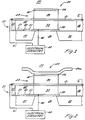
- Figure 1 is a diagram schematically illustrating a first embodiment of an antenna element exemplifying the present invention;
- Fig. 2 is a diagram schematically illustrating a second embodiment of the present invention which includes means for enhancing the vertical aspect of the radiated field;
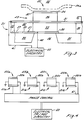
- Fig. 3 is a diagram similar to Figs. 1 and 2 illustrating features of the invention; and
- Fig. 4 is a schematic diagram illustrating a phased array of antenna elements constructed in accordance with the present invention.
- While the invention will be described in connection with certain preferred embodiments, there is no intent to limit it to those embodiments. On the contrary, the intent is to cover all alternatives, modifications and equivalents included within the scope of the invention as defined by the appended claims.
- Turning now to the drawings, Fig. 1 shows an antenna system including an acoustically coupled antenna generally indicated at 20 exemplifying an embodiment of the present invention. The antenna includes a first port (electrical port) generally indicated at 21 connected to
electrical circuitry 22 for interfacing electrical signals between theelectrical circuitry 22 and theantenna 20. Theelectrical circuitry 22 is illustrated as a schematic block, but is typically configured either as a driver portion of a transmitter or the front end of a receiver, or both. Theantenna 20 also has a second port (propagation port) indicated generally at 23, the propagating port including atransducer 24 for interfacing with a propagating medium generally indicated at 25. The propagating medium is typically air and the transducer 24 a conductor which is driven by electrical signals when transmitting, or which receives electromagnetic radiation from the propagatingmedium 25 for producing electrical signals when receiving. - In practicing the invention, the
ports electrical circuitry 22 and thetransducer 24 and from there to the propagatingmedium 25. When used as a transmitter, theelectrical circuitry 22 produces electrical signals which drive thefirst port 21, the signals on thefirst port 21 being acoustically coupled to thesecond port 23 and then retransformed to electrical signals for driving thetransducer 24 and producing electromagnetic radiation in the propagatingmedium 25. When the antenna is used in the receiving mode, electromagnetic radiation in the propagatingmedium 25 is received on theconductive transducer 24 to drive thesecond port 23, the energy in thesecond port 23 is acoustically coupled to thefirst port 21 and retransformed to electrical energy for driving the receiver in theelectrical circuitry 22. - In accordance with the invention, the two port acoustically coupled antenna device is configured as a stacked crystal filter comprising three
electrodes piezoelectric resonators piezoelectric resonators substrate 35 is relieved at 36 as by etching to leave a section of the stacked crystal filter unsupported for free vibration in accordance with the electrical signals imposed on the driven port or ports. It will be apparent to those skilled in this art that the drawing is not to any scale and the thicknesses of the various layers are exaggerated for the purpose of clarity. For example, when the device is used as a transmitter or receiver in the GHz range, thepiezoelectric films - Referring in greater detail to Fig. 1, it is seen that the
electrical circuitry 22 is coupled to thefirst port 21 by means ofelectrical leads electrodes electrode 31 is preferably grounded and the signal imposed on the antenna when thecircuitry 22 is a transmitter or derived from the antenna when thecircuitry 22 is a receiver is carried on theline 40 with respect to ground. - It is seen that the
central electrode 31 is common to both theports electrical port 21 and a ground plane for the transmit/receiver port 23. Thus, theconductive electrode 32 which is grown atop the upperpiezoelectric resonator 34 serves as the transducer for the antenna and is thus electrically conductive for interfacing electromagnetic radiation between the antenna and the propagatingmedium 25. When the system is used as a transmitter, electrical signals are generated in theelectrode 24 which cause electromagnetic propagation into themedium 25 for reception elsewhere. When the system is used as a receiver, electromagnetic radiation in the propagatingmedium 25 causes current flow in theelectrode 24 which is acoustically coupled by means of the stacked crystal filter to theport 21 for passage to theelectrical circuitry 22. - The mechanism by which the energy transfer takes place is the acoustical coupling between the
ports electrical circuitry 22 will generate signals and couple those signals to theelectrodes piezoelectric resonator 33. As will be noted below, the resonator is configured to resonate in the frequency band of interest, and thus, the acoustical energy produced in thepiezoelectric resonator 33 by means of the signals coupled to theelectrodes upper resonator 34. The acoustic energy in theupper resonator 34 will in turn be transformed to electrical signals or current flow in theelectrodes medium 25. - As an important feature of the invention, the characteristics of the stacked crystal filter are configured to match the frequency band of interest for the
antenna 20. That is accomplished primarily by controlling the thicknesses of thepiezoelectric resonators films first port 21 will couple strongly to thesecond port 23 and generate electrical signals in theelectrodes resonators port 21 to theport 23. It will also be apparent that when the antenna is used as a receiver, while the coupling is in the opposite direction, the same principles apply. - As a significant feature of the invention, the shape of the electrodes is preferably configured to shield the
electrical port 21 of the antenna from electromagnetic interference present in the propagatingmedium 25. To that end, thecentral ground electrode 31 is enlarged as compared to the dimensions of the resonators or other electrodes such that the non-common electrode of theelectrical port 21 is shielded by the grounded common electrode. Thus, although electromagnetic interference can be present in the propagatingmedium 25, by virtue of the grounded shield imposed by thecommon electrode 31 in very close (micron) proximity to theelectrode 30, the electromagnetic interference does not couple to theelectrode 30. While the electromagnetic interference can couple to the exposedelectrode 32, since the electromagnetic interference is typically at a frequency other than that for which the antenna is designed, and since the coupling between the ports is acoustical rather than electrical, that further path for introduction of interfering signals is also blocked. Thus, while electromagnetic signals can be imposed on thetransducer 24 to excite theupper resonator 34, since the thicknesses of the resonator are such that the stacked crystal filter will not resonate at those frequencies, the acoustical path for coupling signals to theelectrical port 21 is blocked. In short, the electrical port is blocked first of all by the grounded shield imposed by the common electrode and secondly by the mode of coupling of signals between ports which must resonante in order for coupling to occur. - As is well known in this art, the thin film resonators and particularly stacked crystal filters can be grown on crystalline semiconductor or semiinsulating materials such as silicon or GaAs. Thus, the
substrate 35 illustrated in the drawings is intended to represent such semiconductor or semiinsulating material. In order to allow the stacked crystal filter adequate freedom of movement, as noted above, the substrate is typically etched at 36 below the filter section. Such etching can also be useful in certain embodiments where a separate connection to thelower electrode 30 is desired. In Fig. 1, thelower electrode 30 is illustrated as having a firstextended portion 50 illustrated in solid lines to the left of the stacked crystal filter for providing a location such aspoint 51 for making connections to thelower electrode 30 when it is inconvenient to make connections in the etchedregion 36. It is noted that thesections 52, 53 of the device which bracket thelower resonator 33 are acoustical isolation sections and, for example, can be configured as small etched voids which allow a degree of movement of theresonator 33 for its excitation in the performance of its coupling function. Thus, when thesections 52, 53 are etched, convenient access is provided to the extendedportion 50 of the electrode for making an electrical connection thereto. In a particularly useful configuration of driving circuit and stacked crystal filter on acommon substrate 35, in addition to forming the central stacked crystal filter over the etchedregion 36, positioned exterior of the stacked crystal filter and separated byacoustic isolation regions 52, 53 are extendedportions GaAs substrate 35. Thesections substrate 35 and which themselves can be configured as part of theelectrical circuitry 22. For example, thesection 55 can represent the output of a field effect transistor such as a MOSFET formed on asilicon substrate 35 or a MESFET formed on aGaAs substrate 35, and dottedline extension 57 of theelectrode 50 is intended to indicate a further connection to that output portion of theactive device 55. Such a connection illustrates an important advantage of the antenna according to the present invention in that both the active device which forms theelectrical circuitry 22 and theantenna elements 20 can be monolithically integrated on thesame substrate 35 in order to provide an extremely miniaturized transmission or reception device complete with antenna. Such a device is intended to find significant application in miniaturized personal concealable radio devices intended for operation without detection. - Figs. 2 and 3 illustrate a further embodiment of the invention which is identical to that of Figs. 1 and 3 with the exception of the shape of the electrode which acts as the antenna transducer for coupling to the electromagnetic propagating medium. In the Fig. 2 embodiment (and as illustrated in dashed lines in Fig. 3), the transducer generally indicated at 24 is formed in a complex non-planar shape which, in addition to the basic planar shape of the
electrode 24, includes a shaped portion 24a which extends beyond the plane of theelectrode 24 and also rises from that plane. Typically with a planar array there will be little, if any, gain at the horizon or at the zenith of the antenna. By configuring a section 24a as illustrated in Fig. 2, the antenna is given a vertical aspect which will cause a portion of the energy to be transmitted both to the horizon and to the zenith so that there are no zero gain areas for the antenna. Those skilled in the art of antenna design will appreciate that the shaping of the section 24a will cause the distribution to be altered, and configuration of the antenna in an appropriate shape to achieve the necessary distribution will be apparent to those working in this art. While the section 24a is shown as a further conductive section added to theelectrode 32 which forms thetransducer 24, it will be apparent that theelements 24 and 24a can be grown together by the same evaporation techniques used to form the other electrodes, and need not be separate elements as illustrated in Fig. 2. - Armed with the instant disclosure, the manner of configuring an
antenna 20 to satisfy a particular set of transmitting or receiving conditions will now be apparent to those skilled in the antenna art. It will also be apparent to those skilled in the art that configuring anantenna 20 with separate electrical 21 and radiating 23 ports which are acoustically rather than electrically coupled achieves a certain degree of freedom in configuring theelectrical port 21 to match the electrical characteristics of the coupled circuitry and thepropagation port 23 for matching the radiation resistance experienced by thetransducer 24. Thus, in configuring an antenna according to the invention for a particular application, the electrical impedance of theport 21 is matched to that of the drivingcircuitry 22 utilizing a thickness for thepiezoelectric film 33 which is within the range capable of being tuned to the frequencies of interest. Theelectrical circuitry 22 and drivingport 21 can be matched utilizing those techniques with the major constraint being the limitation on thicknesses of theresonator 33 for achieving resonance of the stacked crystal filter in the desired frequency band. The upper portion of the stacked crystal filter which serves as the radiating port, and particularly the shape of thetransducer 24 is configured to match the driving point impedance of the antenna. Conventional techniques can be used such as use of a network analyzer to determine the driving point scattering matrix and to optimize the shape of thetransducer electrode 24 to shape the radiation pattern in the desired fashion. The very minor thickness of the stacked crystal filter coupled with the isolation provided by the common grounded electrode restricts the radiation field of the antenna to that above theground plane 31 and thus constrains the driving point field to the volume outside of the radiation area defined by theelectrode 24. - Thus, there is a considerable degree of freedom available in designing the radiation portion of the antenna. The primary constraint imposed on the configuration of the
propagation port 23 by the configuration of theelectrical port 21 is that the total thicknesses of the two resonators must be resonant at the frequency of interest. That allows a substantial amount of flexibility in configuring the ports somewhat independently to optimize both with respect to their particular requirements while still achieving highly efficient acoustic coupling between the ports. It will also be apparent that a further degree of freedom is available in allowing the thicknesses of the tworesonators - While the shaped section 24a of the
electrode 24 of Fig. 2 illustrates a particular configuration for enhancing the gain at the zenith and horizon, it more generally illustrates the principle that the size and shape of the transducer which comprises the upper electrode of the stacked crystal filter need not be constrained by the shape of the other electrodes of the stacked crystal filter. It is often desirable that the transducer electrode have about the same or greater area than theelectrical electrode 30 when the device is used as a transmitter so that the transmittingport 23 can extract the maximum amount of the energy coupled into theelectrical port 21 for transmission. When the device is used as a receiver, it may be preferable in many cases to make theelectrode 24 or thecombination electrode 24, 24a as large as possible to provide maximum excitation for theupper resonator 34 in an effort to couple adequate energy to theresonator 33 for extraction at theelectrical port 21. In any event, the drawings of Figs. 1-3 illustrate that the shapes of the electrodes for the respective ports can be independently configured within certain limitations in order to further optimize the respective ports for the functions they are intended to perform. In most events, however, it will be desirable for the commoncentral electrode 31 to be relatively large as compared to the other electrodes for providing an adequate ground plane for thetransducer electrode 24 and adequate shielding for theelectrical port 21 from electromagnetic radiation. - Turning now to Fig. 4, there is illustrated a further embodiment of the present invention utilizing a plurality of antenna elements 20a-20n configured in an array of predetermined dimension and operated as a phased array. For example, the antennas 20a-20n are typically configured in a linear array at predetermined spacing, and are driven by electrical signals adjusted in phase to steer a beam normal to the array at any desired position in the plane normal to the array.
- To that end, the normal transmit or receive circuitry is illustrated as 60 and is coupled to an intermediate phase control circuit 61 which in turn drives the electrical ports 21a-21n with the same signal but at different phases of that signal for the purposes of steering. Thus, when used as a transmitter, the signal is propagated through the transmitting
ports 23a-23n with the phase delayed from radiator to radiator within the array, and with the phase being adjusted from pulse to pulse of transmitted energy to cause the steering of the beam from the phased array. Similarly, when the array is used in a receiving mode, signals received at the individual antenna elements are coupled to the electrical circuitry in phase differentiation as controlled by signals from the phase control circuit 61 such that the received signal is selected from any point in the plane perpendicular to the array as determined by the relative phasing between the received signals. The phased array itself will not be explained further herein since such technic es for steered beam radar and the like are well known to those skilled in the art. What will be now apparent to those skilled in the art, however, is that such a phased array can be achieved with significant isolation between the phase control electrical elements of the control electronics and the transmitting or receiving transducer elements of the antenna, with the coupling between such elements being accomplished acoustically to achieve the independent degrees of freedom in configuring the respective ports and the isolation between the ports described in detail above. - It will now be apparent that what has been provided is a new configuration of antenna which has a first port for coupling to electrical circuitry which is typically a transmitter or a receiver and a second pc t for interfacing with a propagating medium. Each port has electrodes for coupling to the respective elements, with one of the electrodes of the port coupled to the propagating medium serving as the transmitting or receiving transducer. The ports are electrically isolated but acoustically coupled so that the energy which is passed between the electrical elements coupled to one port and the electromagnetic radiating elements coupled to the other port are interfaced only by way of the acoustical coupling. Acoustical coupling is accomplished by means of a stacked crystal filter which is tuned to the passband at which the antenna is intended to operate, so as to couple energy at maximum efficiency between the ports in the passband of the antenna but to sharply reject energy out of the band. Susceptibility to electromagnetic interference, which is provided in one measure by virtue of the acoustic rather than electrical coupling, is further enhanced by configuring a common electrode between the elements of the stacked crystal filter as an extended ground plane which constrains the driving point field of the transducer section of the antenna to the volume outside the radiating area.
Claims (16)
- An antenna device (20) for coupling energy in a predetermined frequency band between electrical circuitry (22) and an electromagnetic propagating medium (25), and comprising:a first port (21) coupled to and electrically matched in the predetermined frequency band to the electrical circuity (25) for exchanging energy therewith,a second port (23) having a transducer (24) for interfacing between the antenna device (20) and the propagating medium (25), the transducer (24) serving to convert between electrical signals in the transducer (24) and electromagnetic radiation in the propagating medium (25),and acoustical coupling means (30-34) for acoustically coupling the first (21) and second (23) ports, the acoustical coupling means (30-34) serving to translate between electrical energy in the predetermined frequency band at the ports (21,23) and acoustical energy for coupling between the ports (21,23), characterised in thatthe acoustical coupling means (30-34) includes a thin film resonator having piezoelectric resonator means (33,34) comprising thin film dielectric layer means (33,34) adapted to resonate at frequencies in a predetermined elevated frequency band, the first port includes first thin film electrode means (30,31) formed on the piezoelectric resonator means (33) and connected to the electrical circuitry (22) for transforming between electrical energy in the electrical circuitry and acoustical energy in the piezoelectric resonator means (33), the second port (23) includes second thin film electrode means (31,32) formed on the piezoelectric resonator means (34), and said second electrode means (32) itself serves as the transducer (24) and directly couples energy between the propagating medium (25) and the piezoelectric resonator means (33,34).
- An antenna device as set forth in claim 1, wherein the first port (21) comprises a pair of electrodes (30,31) separated by a first piezoelectric resonator (33), and the second port (23) comprises a pair of electrodes (31,32) separated by a second piezoelectric resonator (34), one of the electrodes of the first (21) and second (23) ports being a common electrode (31) disposed in both said ports, whereby the piezoelectric resonators (33,34) separated by the common electrode (31) serve as the coupling means between the ports (21,23), and the non-common electrode (32) of the second ports (23) serves as said transducer (24) for directly coupling energy between the piezoelectric resonators (33,34) and the propagating medium (25).
- An antenna device as set forth in claim 1, wherein the ports (21,23) and the acoustic coupling means (33,34) are configured as a stacked crystal filter (30-34) comprising three thin film electrodes (30-32) disposed on and separated by first (33) and second (34) thin film piezoelectric resonating elements, a central one (31) of the three electrodes (30-32) being shared by the two ports (21,23), and the piezoelectric resonators (33,34) being acoustically coupled for acoustically coupling energy between the ports and translating the coupled energy to or from electrical energy at the ports (21,23).
- An antenna device as set forth in claim 3, wherein the electrical circuitry (22) and stacked crystal filter (30-34) are supported on a common semiconductor or semi-insulator substrate (35).
- A phased antenna array (30a-20n) comprising a plurality of antenna devices (20a-20n) as set forth in claim 3, and wherein the electrical circuitry (60) includes phase control means (61) for phasing the devices (20a-20n) in the antenna array.
- An antenna device as set forth in claim 1, wherein the piezoelectric resonator means (33,34) includes first and second coupled piezoelectric resonators (30-34), the first thin film electrode means (30,31) being formed on the first piezoelectric resonator (33) and serving as the first port (21), the second port (23) including the second piezoelectric resonator (34), coupled to the first (33), and having the second thin film electrode means (31,32) formed thereon and located in the propagating medium (25) to serve as the transducer (24), and the first and second thin film electrode means (30-32) including a common electrode (31) shared by the first and second coupled resonators (33,34).
- An antenna device as set forth in claim 6, wherein the first and second ports (21,23) and the acoustic coupling means (30-34) comprise a thin film stacked crystal filter (30-34), the stacked crystal filter (30-34) including the first and second coupled thin film piezoelectric resonators (33,34) separated by the common electrode (31) and sandwiched by first (30) and second (32) thin film electrodes,the first (30) and common (31) electrodes associated wiuth the first piezoelectric resonator (33) including connecting means (40,41) for coupling to the electrical circuitry (22) for interfacing electrical energy in the predetermined frequency band therewith,and the second electrode (32) associated with the second piezoelecctric resonator (34) forming said transducer (24) for directly coupling energy between the second port (23) and the propagating medium (25) in the predetermined frequency band.
- An antenna device as set forth in claim 7, wherein the common electrode (31) is grounded and serves as a shield against electromagnetic interference protecting said first port (21) from electromagnetic radiation outside of the predetermined frequency band.
- An antenna device as set forth in claim 8, wherein the grounded common electrode (31) serves as a ground plane for the said transducer.
- An antenna device as set forth in claim 7, wherein the device (20) is a transmitting antenna, the electrical circuitry (22) being a transmitter driver for connection to the first port (21) for exciting the first piezoelectric resonator (33) therein, the transducer (24) being a radiator of electromagnetic energy in the predetermined frequency band, and the coupling means (30-34) serving to couple acoustic energy from the first piezoelectric resonator (33) to the second piezoelectric resonator (34) and translate said coupled acoustical energy into electrical energy in the second port (23) for radiation by the transducer (24).
- An antenna device as set forth in claim 7, wherein the device (20) is a receiving antenna, the electrical circuitry (22) being an electrical receiver for receiving electrical signals from the first port (21), the transducer (24) in the second port (23) being adapted to receive electromagnetic energy from the propagating medium (25) and excite the second piezoelectric resonator (34), and the coupling means (30-34) serving to couple acoustical energy from the second (34) to the first (33) piezoelectric resonator for translation into electrical signals by the first piezoelectric resonator (33) and coupling to said electrical circuitry (22).
- An antenna device as set forth in claim 7, wherein the electrical circuitry (22) and stacked crystal filter (30-34) are supported on a common semiconductor or semi-insulator substrate (35).
- A phased antenna array (20a-20n) comprising a plurality of antenna devices (20a-20n) as set forth in claim 7, and wherein the electrical circuitry (60) includes phase control means (61) for phasing the devices (20a-20n) in the antenna array.
- An antenna device as set forth in claim 1, wherein the acoustical coupling means (30-34) is configured as a stacked crystal filter (30-34) comprising first, second and third thin film electrodes (30-32), and first and second thin film piezoelectric elements (33,34) interposed respectively between the first (30) and second (31) electrodes and the second (31) and third (32) electrodes,the first and second electrodes (30-31) and first piezoelectric element (33) therebetween serving as the first port (21) for coupling to the electrical circuitry (22) and transforming between electrical energy in the electrical circuitry (22) and acoustical energy in the piezoelectric elements (33,34),the second and third electrodes (31,32) and second piezoelectric element (34) therebetween serving as the second port (23) for coupling to the propagating medium (25) and transforming between acoustical energy in the piezoelectric elements (33,34) and electromagnetic energy in the propagating medium (25), the third electrode (32) being disposed in the propagating medium (25) for translating between electromagnetic radiation in the medium (25) and electrical energy in the electrode (32),and the piezoelectric elements (33,334) being resonant in the predetermined frequency band of the antenna (20) for acoustically coupling the first and second ports (21,23) in the predetermined frequency band for selectively passing energy therebetween in said frequency band.
- An antenna device as set forth in claim 14, wherein the electrical circuitry (22) and stacked crystal filter (30-34) are supported on a common semiconductor or semi-insulator substrate (35).
- A phased antenna array (20a-20n) comprising a plurality of antenna devices (20a-20n) as set forth in claim 14, and wherein the electrical circuitry (60) includes phase control means (61) for phasing the devices (20a-20n) in the antenna array.
Applications Claiming Priority (3)
| Application Number | Priority Date | Filing Date | Title |
|---|---|---|---|
| US359517 | 1982-03-18 | ||
| US07/359,517 US5034753A (en) | 1989-06-01 | 1989-06-01 | Acoustically coupled antenna |
| PCT/US1990/003010 WO1990015479A1 (en) | 1989-06-01 | 1990-05-30 | Acoustically coupled antenna |
Publications (3)
| Publication Number | Publication Date |
|---|---|
| EP0474788A1 EP0474788A1 (en) | 1992-03-18 |
| EP0474788A4 EP0474788A4 (en) | 1992-09-23 |
| EP0474788B1 true EP0474788B1 (en) | 1996-04-24 |
Family
ID=23414157
Family Applications (1)
| Application Number | Title | Priority Date | Filing Date |
|---|---|---|---|
| EP90911019A Expired - Lifetime EP0474788B1 (en) | 1989-06-01 | 1990-05-30 | Acoustically coupled antenna |
Country Status (6)
| Country | Link |
|---|---|
| US (1) | US5034753A (en) |
| EP (1) | EP0474788B1 (en) |
| JP (1) | JPH04505691A (en) |
| CA (1) | CA2056367A1 (en) |
| DE (1) | DE69026713T2 (en) |
| WO (1) | WO1990015479A1 (en) |
Families Citing this family (18)
| Publication number | Priority date | Publication date | Assignee | Title |
|---|---|---|---|---|
| US5294898A (en) * | 1992-01-29 | 1994-03-15 | Motorola, Inc. | Wide bandwidth bandpass filter comprising parallel connected piezoelectric resonators |
| US5650685A (en) * | 1992-01-30 | 1997-07-22 | The United States Of America As Represented By The Secretary Of The Army | Microcircuit package with integrated acoustic isolator |
| US5361077A (en) * | 1992-05-29 | 1994-11-01 | Iowa State University Research Foundation, Inc. | Acoustically coupled antenna utilizing an overmoded configuration |
| US5367308A (en) * | 1992-05-29 | 1994-11-22 | Iowa State University Research Foundation, Inc. | Thin film resonating device |
| US5760706A (en) * | 1993-10-29 | 1998-06-02 | Kiss; Michael Z. | Remote control system using partially earth-buried RF antenna |
| US5883575A (en) * | 1997-08-12 | 1999-03-16 | Hewlett-Packard Company | RF-tags utilizing thin film bulk wave acoustic resonators |
| US7531079B1 (en) | 1998-10-26 | 2009-05-12 | Novellus Systems, Inc. | Method and apparatus for uniform electropolishing of damascene IC structures by selective agitation |
| US6709565B2 (en) | 1998-10-26 | 2004-03-23 | Novellus Systems, Inc. | Method and apparatus for uniform electropolishing of damascene ic structures by selective agitation |
| US7449098B1 (en) | 1999-10-05 | 2008-11-11 | Novellus Systems, Inc. | Method for planar electroplating |
| US6653226B1 (en) * | 2001-01-09 | 2003-11-25 | Novellus Systems, Inc. | Method for electrochemical planarization of metal surfaces |
| US6377137B1 (en) * | 2000-09-11 | 2002-04-23 | Agilent Technologies, Inc. | Acoustic resonator filter with reduced electromagnetic influence due to die substrate thickness |
| US7799200B1 (en) | 2002-07-29 | 2010-09-21 | Novellus Systems, Inc. | Selective electrochemical accelerator removal |
| US8530359B2 (en) | 2003-10-20 | 2013-09-10 | Novellus Systems, Inc. | Modulated metal removal using localized wet etching |
| US8158532B2 (en) * | 2003-10-20 | 2012-04-17 | Novellus Systems, Inc. | Topography reduction and control by selective accelerator removal |
| EP1988575A3 (en) * | 2007-03-26 | 2008-12-31 | Semiconductor Energy Laboratory Co., Ltd. | Semiconductor device |
| CN101971493A (en) * | 2007-12-20 | 2011-02-09 | D·辛哈 | micro antenna device |
| RU2528243C2 (en) | 2009-06-03 | 2014-09-10 | Конинклейке Филипс Электроникс Н.В. | Terahertz antenna |
| US8168540B1 (en) | 2009-12-29 | 2012-05-01 | Novellus Systems, Inc. | Methods and apparatus for depositing copper on tungsten |
Family Cites Families (8)
| Publication number | Priority date | Publication date | Assignee | Title |
|---|---|---|---|---|
| US2313850A (en) * | 1941-02-08 | 1943-03-16 | Rca Corp | Radio transmitter |
| GB736563A (en) * | 1953-06-06 | 1955-09-07 | Ferranti Ltd | Improvements relating to electrical filters |
| US2976501A (en) * | 1959-07-30 | 1961-03-21 | Oskar E Mattiat | Impedance transformer |
| DE1443849A1 (en) * | 1963-03-06 | 1968-11-07 | Bayer Ag | Process for the preparation of unsaturated acid amides containing sulfone groups |
| US4072846A (en) * | 1976-03-01 | 1978-02-07 | Varian Associates, Inc. | Control system for a chromatography apparatus oven door |
| JPS54120592A (en) * | 1977-12-09 | 1979-09-19 | Lintech Instr Ltd | Transponder |
| US4320365A (en) * | 1980-11-03 | 1982-03-16 | United Technologies Corporation | Fundamental, longitudinal, thickness mode bulk wave resonator |
| GB2189080B (en) * | 1986-04-02 | 1989-11-29 | Thorn Emi Electronics Ltd | Microstrip antenna |
-
1989
- 1989-06-01 US US07/359,517 patent/US5034753A/en not_active Expired - Fee Related
-
1990
- 1990-05-30 CA CA002056367A patent/CA2056367A1/en not_active Abandoned
- 1990-05-30 EP EP90911019A patent/EP0474788B1/en not_active Expired - Lifetime
- 1990-05-30 JP JP2510357A patent/JPH04505691A/en active Pending
- 1990-05-30 WO PCT/US1990/003010 patent/WO1990015479A1/en not_active Ceased
- 1990-05-30 DE DE69026713T patent/DE69026713T2/en not_active Expired - Fee Related
Also Published As
| Publication number | Publication date |
|---|---|
| CA2056367A1 (en) | 1990-12-02 |
| US5034753A (en) | 1991-07-23 |
| WO1990015479A1 (en) | 1990-12-13 |
| EP0474788A4 (en) | 1992-09-23 |
| DE69026713T2 (en) | 1996-11-28 |
| EP0474788A1 (en) | 1992-03-18 |
| JPH04505691A (en) | 1992-10-01 |
| DE69026713D1 (en) | 1996-05-30 |
Similar Documents
| Publication | Publication Date | Title |
|---|---|---|
| US5034753A (en) | Acoustically coupled antenna | |
| US5361077A (en) | Acoustically coupled antenna utilizing an overmoded configuration | |
| US5386215A (en) | Highly efficient planar antenna on a periodic dielectric structure | |
| US4573212A (en) | Integrated receiver antenna device | |
| US6191740B1 (en) | Slot fed multi-band antenna | |
| US5453754A (en) | Dielectric resonator antenna with wide bandwidth | |
| US5940036A (en) | Broadband circularly polarized dielectric resonator antenna | |
| US5617103A (en) | Ferroelectric phase shifting antenna array | |
| US5243353A (en) | Circularly polarized broadband microstrip antenna | |
| EP0587247B1 (en) | Dielectric resonator antenna with wide bandwidth | |
| US8144059B2 (en) | Active dielectric resonator antenna | |
| JPH10224141A (en) | Monolithic antenna | |
| US7394334B2 (en) | Dielectric resonance apparatus, oscillation apparatus, and transmission/reception apparatus | |
| US12489226B2 (en) | Dual-frequency band dual-circularly polarized antenna and antenna system | |
| JP3764877B2 (en) | Radar equipment | |
| WO2012131376A1 (en) | Apparatus and methods | |
| EP0767531B1 (en) | A microwave oscillation circuit and a down converter using the same | |
| Weber | Acoustically coupled antenna | |
| JP7618063B2 (en) | Composite Antenna | |
| US20020132601A1 (en) | Non-radiative dielectric waveguide mixer using a ring hybrid coupler | |
| JPH11145722A (en) | Microstrip antenna | |
| JPH08335827A (en) | Antenna device | |
| JPH0590826A (en) | Micro strip antenna | |
| JPH0998005A (en) | Wiring board | |
| WO2009082300A1 (en) | Tuneable antenna arrangement |
Legal Events
| Date | Code | Title | Description |
|---|---|---|---|
| PUAI | Public reference made under article 153(3) epc to a published international application that has entered the european phase |
Free format text: ORIGINAL CODE: 0009012 |
|
| 17P | Request for examination filed |
Effective date: 19911031 |
|
| AK | Designated contracting states |
Kind code of ref document: A1 Designated state(s): DE FR GB |
|
| A4 | Supplementary search report drawn up and despatched |
Effective date: 19920804 |
|
| AK | Designated contracting states |
Kind code of ref document: A4 Designated state(s): DE FR GB |
|
| 17Q | First examination report despatched |
Effective date: 19941118 |
|
| GRAA | (expected) grant |
Free format text: ORIGINAL CODE: 0009210 |
|
| AK | Designated contracting states |
Kind code of ref document: B1 Designated state(s): DE FR GB |
|
| REF | Corresponds to: |
Ref document number: 69026713 Country of ref document: DE Date of ref document: 19960530 |
|
| ET | Fr: translation filed | ||
| PLBE | No opposition filed within time limit |
Free format text: ORIGINAL CODE: 0009261 |
|
| STAA | Information on the status of an ep patent application or granted ep patent |
Free format text: STATUS: NO OPPOSITION FILED WITHIN TIME LIMIT |
|
| 26N | No opposition filed | ||
| PGFP | Annual fee paid to national office [announced via postgrant information from national office to epo] |
Ref country code: FR Payment date: 19970513 Year of fee payment: 8 |
|
| PGFP | Annual fee paid to national office [announced via postgrant information from national office to epo] |
Ref country code: GB Payment date: 19970521 Year of fee payment: 8 |
|
| PGFP | Annual fee paid to national office [announced via postgrant information from national office to epo] |
Ref country code: DE Payment date: 19970606 Year of fee payment: 8 |
|
| PG25 | Lapsed in a contracting state [announced via postgrant information from national office to epo] |
Ref country code: GB Free format text: LAPSE BECAUSE OF NON-PAYMENT OF DUE FEES Effective date: 19980530 |
|
| PG25 | Lapsed in a contracting state [announced via postgrant information from national office to epo] |
Ref country code: FR Free format text: LAPSE BECAUSE OF NON-PAYMENT OF DUE FEES Effective date: 19980531 |
|
| GBPC | Gb: european patent ceased through non-payment of renewal fee |
Effective date: 19980530 |
|
| PG25 | Lapsed in a contracting state [announced via postgrant information from national office to epo] |
Ref country code: DE Free format text: LAPSE BECAUSE OF NON-PAYMENT OF DUE FEES Effective date: 19990302 |
|
| REG | Reference to a national code |
Ref country code: FR Ref legal event code: ST |