EP0473058A2 - Liquid crystal apparatus - Google Patents
Liquid crystal apparatus Download PDFInfo
- Publication number
- EP0473058A2 EP0473058A2 EP91114021A EP91114021A EP0473058A2 EP 0473058 A2 EP0473058 A2 EP 0473058A2 EP 91114021 A EP91114021 A EP 91114021A EP 91114021 A EP91114021 A EP 91114021A EP 0473058 A2 EP0473058 A2 EP 0473058A2
- Authority
- EP
- European Patent Office
- Prior art keywords
- liquid crystal
- voltage signal
- applying
- gradation
- wiring lines
- Prior art date
- Legal status (The legal status is an assumption and is not a legal conclusion. Google has not performed a legal analysis and makes no representation as to the accuracy of the status listed.)
- Granted
Links
- 239000004973 liquid crystal related substance Substances 0.000 title claims abstract description 110
- 230000010287 polarization Effects 0.000 claims abstract description 45
- 230000002269 spontaneous effect Effects 0.000 claims abstract description 38
- 230000005684 electric field Effects 0.000 claims abstract description 15
- 230000001747 exhibiting effect Effects 0.000 claims abstract description 15
- 239000005262 ferroelectric liquid crystals (FLCs) Substances 0.000 claims description 25
- 230000003287 optical effect Effects 0.000 claims description 21
- 230000004044 response Effects 0.000 claims description 16
- 239000000758 substrate Substances 0.000 claims description 8
- 239000002131 composite material Substances 0.000 claims description 6
- 230000004807 localization Effects 0.000 description 29
- 238000000034 method Methods 0.000 description 12
- 239000011159 matrix material Substances 0.000 description 11
- 210000004027 cell Anatomy 0.000 description 9
- 150000002500 ions Chemical class 0.000 description 8
- 238000010586 diagram Methods 0.000 description 7
- 230000033001 locomotion Effects 0.000 description 5
- 238000002834 transmittance Methods 0.000 description 5
- 239000010409 thin film Substances 0.000 description 4
- 230000015572 biosynthetic process Effects 0.000 description 3
- 238000002474 experimental method Methods 0.000 description 3
- 239000004990 Smectic liquid crystal Substances 0.000 description 2
- 230000000694 effects Effects 0.000 description 2
- 239000010408 film Substances 0.000 description 2
- 239000010936 titanium Substances 0.000 description 2
- 239000004642 Polyimide Substances 0.000 description 1
- RTAQQCXQSZGOHL-UHFFFAOYSA-N Titanium Chemical compound [Ti] RTAQQCXQSZGOHL-UHFFFAOYSA-N 0.000 description 1
- 229910021417 amorphous silicon Inorganic materials 0.000 description 1
- 230000005540 biological transmission Effects 0.000 description 1
- 230000001276 controlling effect Effects 0.000 description 1
- 210000002858 crystal cell Anatomy 0.000 description 1
- 230000003247 decreasing effect Effects 0.000 description 1
- 230000006866 deterioration Effects 0.000 description 1
- 230000006870 function Effects 0.000 description 1
- 230000001771 impaired effect Effects 0.000 description 1
- 230000014759 maintenance of location Effects 0.000 description 1
- 239000000463 material Substances 0.000 description 1
- 238000005259 measurement Methods 0.000 description 1
- 239000000203 mixture Substances 0.000 description 1
- 229910021420 polycrystalline silicon Inorganic materials 0.000 description 1
- 229920001721 polyimide Polymers 0.000 description 1
- 229920005591 polysilicon Polymers 0.000 description 1
- 230000001105 regulatory effect Effects 0.000 description 1
- 239000004065 semiconductor Substances 0.000 description 1
- 229910052710 silicon Inorganic materials 0.000 description 1
- 239000010703 silicon Substances 0.000 description 1
- 229910052814 silicon oxide Inorganic materials 0.000 description 1
- 230000000087 stabilizing effect Effects 0.000 description 1
- 229910052719 titanium Inorganic materials 0.000 description 1
Images


Classifications
-
- H—ELECTRICITY
- H04—ELECTRIC COMMUNICATION TECHNIQUE
- H04N—PICTORIAL COMMUNICATION, e.g. TELEVISION
- H04N3/00—Scanning details of television systems; Combination thereof with generation of supply voltages
- H04N3/10—Scanning details of television systems; Combination thereof with generation of supply voltages by means not exclusively optical-mechanical
- H04N3/12—Scanning details of television systems; Combination thereof with generation of supply voltages by means not exclusively optical-mechanical by switched stationary formation of lamps, photocells or light relays
- H04N3/122—Scanning details of television systems; Combination thereof with generation of supply voltages by means not exclusively optical-mechanical by switched stationary formation of lamps, photocells or light relays using cathode rays, e.g. multivision
-
- G—PHYSICS
- G09—EDUCATION; CRYPTOGRAPHY; DISPLAY; ADVERTISING; SEALS
- G09G—ARRANGEMENTS OR CIRCUITS FOR CONTROL OF INDICATING DEVICES USING STATIC MEANS TO PRESENT VARIABLE INFORMATION
- G09G3/00—Control arrangements or circuits, of interest only in connection with visual indicators other than cathode-ray tubes
- G09G3/20—Control arrangements or circuits, of interest only in connection with visual indicators other than cathode-ray tubes for presentation of an assembly of a number of characters, e.g. a page, by composing the assembly by combination of individual elements arranged in a matrix no fixed position being assigned to or needed to be assigned to the individual characters or partial characters
- G09G3/34—Control arrangements or circuits, of interest only in connection with visual indicators other than cathode-ray tubes for presentation of an assembly of a number of characters, e.g. a page, by composing the assembly by combination of individual elements arranged in a matrix no fixed position being assigned to or needed to be assigned to the individual characters or partial characters by control of light from an independent source
- G09G3/36—Control arrangements or circuits, of interest only in connection with visual indicators other than cathode-ray tubes for presentation of an assembly of a number of characters, e.g. a page, by composing the assembly by combination of individual elements arranged in a matrix no fixed position being assigned to or needed to be assigned to the individual characters or partial characters by control of light from an independent source using liquid crystals
- G09G3/3611—Control of matrices with row and column drivers
- G09G3/3648—Control of matrices with row and column drivers using an active matrix
- G09G3/3651—Control of matrices with row and column drivers using an active matrix using multistable liquid crystals, e.g. ferroelectric liquid crystals
-
- G—PHYSICS
- G09—EDUCATION; CRYPTOGRAPHY; DISPLAY; ADVERTISING; SEALS
- G09G—ARRANGEMENTS OR CIRCUITS FOR CONTROL OF INDICATING DEVICES USING STATIC MEANS TO PRESENT VARIABLE INFORMATION
- G09G2310/00—Command of the display device
- G09G2310/06—Details of flat display driving waveforms
-
- G—PHYSICS
- G09—EDUCATION; CRYPTOGRAPHY; DISPLAY; ADVERTISING; SEALS
- G09G—ARRANGEMENTS OR CIRCUITS FOR CONTROL OF INDICATING DEVICES USING STATIC MEANS TO PRESENT VARIABLE INFORMATION
- G09G2310/00—Command of the display device
- G09G2310/06—Details of flat display driving waveforms
- G09G2310/061—Details of flat display driving waveforms for resetting or blanking
-
- G—PHYSICS
- G09—EDUCATION; CRYPTOGRAPHY; DISPLAY; ADVERTISING; SEALS
- G09G—ARRANGEMENTS OR CIRCUITS FOR CONTROL OF INDICATING DEVICES USING STATIC MEANS TO PRESENT VARIABLE INFORMATION
- G09G2310/00—Command of the display device
- G09G2310/06—Details of flat display driving waveforms
- G09G2310/065—Waveforms comprising zero voltage phase or pause
-
- G—PHYSICS
- G09—EDUCATION; CRYPTOGRAPHY; DISPLAY; ADVERTISING; SEALS
- G09G—ARRANGEMENTS OR CIRCUITS FOR CONTROL OF INDICATING DEVICES USING STATIC MEANS TO PRESENT VARIABLE INFORMATION
- G09G3/00—Control arrangements or circuits, of interest only in connection with visual indicators other than cathode-ray tubes
- G09G3/20—Control arrangements or circuits, of interest only in connection with visual indicators other than cathode-ray tubes for presentation of an assembly of a number of characters, e.g. a page, by composing the assembly by combination of individual elements arranged in a matrix no fixed position being assigned to or needed to be assigned to the individual characters or partial characters
- G09G3/2007—Display of intermediate tones
- G09G3/2011—Display of intermediate tones by amplitude modulation
-
- G—PHYSICS
- G09—EDUCATION; CRYPTOGRAPHY; DISPLAY; ADVERTISING; SEALS
- G09G—ARRANGEMENTS OR CIRCUITS FOR CONTROL OF INDICATING DEVICES USING STATIC MEANS TO PRESENT VARIABLE INFORMATION
- G09G3/00—Control arrangements or circuits, of interest only in connection with visual indicators other than cathode-ray tubes
- G09G3/20—Control arrangements or circuits, of interest only in connection with visual indicators other than cathode-ray tubes for presentation of an assembly of a number of characters, e.g. a page, by composing the assembly by combination of individual elements arranged in a matrix no fixed position being assigned to or needed to be assigned to the individual characters or partial characters
- G09G3/2007—Display of intermediate tones
- G09G3/207—Display of intermediate tones by domain size control
Definitions
- the present invention relates to a liquid crystal apparatus exhibiting spontaneous polarization and, more particularly, to a liquid crystal apparatus using a ferroelectric liquid crystal (FLC).
- FLC ferroelectric liquid crystal
- a ferroelectric liquid crystal (FLC) as a liquid crystal exhibiting the spontaneous polarization has received a great deal of attention in favor of advantages such as high-speed response and good memory characteristics and has been actively developed to obtain a light bulb and the like.
- Targets utilizing the above advantages are an optical shutter array, a high-definition display unit by simple matrix driving, a light bulb for high-density recording combined with a photoconductive body.
- the ferroelectric liquid crystal is expected to display a motion picture by active matrix driving using thin film transistors (TFTs).
- One of the problems is a decrease in response speed of the liquid crystal when a direct current (DC) component is continuously applied to the FLC for a long period of time due to the following reason. Localization of internal ions in the liquid crystal is assumed to be induced to form an electric field.
- DC direct current
- a liquid crystal apparatus comprising a pair of electrodes, a liquid crystal panel having a liquid crystal arranged between the pair of electrodes and exhibiting spontaneous polarization, first means for applying a gradation voltage signal corresponding to gradation information to the pair of electrodes, and second means for applying, a DC component serving as a reverse bias for an internal electric field generated upon application of the gradation voltage signal, to the liquid crystal during one vertical scanning period.
- a liquid crystal element comprising a liquid crystal exhibiting spontaneous polarization, a pair of electrode substrates for sandwiching the liquid crystal therebetween, and insulating layers formed between the liquid crystal and the pair of electrode substrates, wherein the following condition is established between a spontaneous polarization P s value of the liquid crystal, an interelectrode composite capacitance Ci of the insulating layers, and a threshold voltage value Vth of an optical response of the liquid crystal in the liquid crystal element:
- a liquid crystal panel used in the present invention is a liquid crystal panel of an active matrix drive scheme, as shown in Fig. 17.
- the liquid crystal panel comprises switching elements (TFTs obtained by using thin film semiconductors such as amorphous silicon and polysilicon) arranged along a plurality of rows (scanning lines) and a plurality of columns (data lines), first wiring lines (gate lines) commonly connecting the first terminals (gates) of the switching elements in units of rows, second wiring lines (source lines) connecting the second terminals (sources) of the switching elements in units of columns, a plurality of pixel electrodes (transparent electrodes) connected in units of third terminals (drains) of the switching elements, counter electrodes (transparent electrodes) arranged to oppose the pixel electrodes, and a liquid crystal (chiral smectic C, H, I, G, F liquid crystal exhibiting ferroelectric properties) exhibiting spontaneous polarization and arranged between the plurality of pixel electrodes and the counter electrodes.
- switching elements TFTs obtained by
- the distance between each pixel electrode and the corresponding counter electrode is set to be a minimum distance (about 5 ⁇ m or less) capable of sufficiently suppressing formation of a helical structure of the chiral smectic liquid crystal.
- the formation of the helical structure need not be suppressed in the present invention.
- Thermal control may be performed during driving of the liquid crystal to maintain the liquid crystal within a desired temperature range.
- an auxiliary voltage signal V sx having a magnitude corresponding to that of the recording voltage signal V W is applied, thereby controlling an internal electric field to be described below.
- Figs. 2A and 2B show a pseudo equivalent circuit model of an FLC element.
- Fig. 3 shows an ionic localization diagram obtained when an external DC component is applied for a long period of time.
- a positive external DC component is applied, it is assumed that ionic localization indicated by ⁇ and ⁇ occurs inside the liquid crystal layer.
- P s spontaneous polarization
- Figs. 4A and 4B show ionic localization by spontaneous polarization (PS) itself.
- PS spontaneous polarization
- the DC component can be controlled by an external voltage applied to the liquid crystal.
- the auxiliary voltage V S serves as a DC component, and the ionic localization is kept “constant” regardless of the state of the spontaneous polarization P S .
- the term “constant” indicates a total amount of ionic localization.
- the “constant” value may be a predetermined value or zero. However, the “constant” value need not always be zero.
- a method of adjusting the ionic localization to be "constant" will be described with reference to Figs. 5A to 5C.
- a total amount of ionic localization is apparently maintained to be an amount with which the "black" state as shown in Fig. 4A is kept set.
- the ionic localization sate of the "black" state shown in Fig. 5A is taken as an initial state.
- a drive signal having a waveform shown in Fig. 1(a) is applied to the liquid crystal in advance.
- a drive signal having a waveform shown in Fig. 6A is applied to obtain the "black” state.
- the superposition amount of the DC component by the auxiliary voltage V SX may be zero.
- the ionic localization state to be obtained by this display is as shown in Fig. 18A.
- an auxiliary voltage +V SX1 shown in Fig. 6A is applied to add the ionic localization of Fig. 18B.
- an auxiliary voltage +V SX2 (Fig. 6C) is applied to maintain the state of Fig. 19A (i.e., the ionic localization state formed by this display) to the total amount obtained in the case of the "black" display.
- the numerical control of the auxiliary voltages V SX1 and V SX2 is appropriately performed in accordance with the magnitude of the instantaneous polarization P S and the ambient temperature. It is advantageous if the magnitude of the spontaneous polarization P S is set not so large (i.e., 10 nC/cm2 or less, and preferably 5 nC/cm2 or less) in the liquid crystal used in the present invention since then an excessive increase in the amplitude of the auxiliary voltage signal V SX can be suppressed.
- the numerical value for the amplitude of the signal V SX1 preferably falls within the following range: (where ⁇ a is the gradation at the end of application of the voltage V W and satisfies condition 0 ⁇ ⁇ a ⁇ 1, and Ci is the capacitance of the insulating layer)
- ⁇ a is the gradation at the end of application of the voltage V W and satisfies condition 0 ⁇ ⁇ a ⁇ 1
- Ci is the capacitance of the insulating layer
- the divided voltage of the liquid crystal layer is given as follows: Since a voltage which causes movement of ions in this gradation state is given by the above relation, if an external reverse voltage V SX of the voltage which causes this movement of ions is applied and the divided voltage of the liquid crystal by the voltage V SX is set to equal to movement of ions is assumed not to occur. Therefore, the following equation is established: and the solution can be obtained as follows:
- V SX about 0.5 V can be obtained even in the full "white" state.
- the initial ionic localization state can be maintained constant.
- the DC component also serves as a "white" retention voltage of the liquid crystal, high-speed response of the liquid crystal can be obtained and can cope with the motion picture.
- Figs. 10 and 11 show an optical response test improved by the above driving method.
- the peak value of the auxiliary voltage is preferably stabilized.
- the maximum value of the voltage V SX is preferably set as follows: The present invention proposes the optical element on the basis of the findings that the above condition must be essentially satisfied to balance the ions.
- the effective magnitude of the spontaneous polarization P S of the liquid crystal used and the composite capacitance Ci of the alignment layers as important components constituting the element or an insulating layer portion including an additional insulating layer in the element must satisfy the above permanent relationship, thereby performing substantially stable gradation driving.
- the composite capacitance Ci is preferably set to be large, and the spontaneous polarization value P S of the liquid crystal used is preferably set to be small.
- insulating layers formed to prevent electrical short-circuiting of the upper and lower electrodes of each cell are formed such that an oxide mixture (Ti-SiO X ) of Ti (titanium) and Si (silicon) is coated on the electrodes and baked to obtain thin films each having a thickness of about 1,000 ⁇ .
- a 200 ⁇ thick polyimide alignment layer is formed on this insulating film and baked.
- the resultant structure is rubbed to maximize the composite capacitance Ci.
- the capacitance Ci can be about several 10 nF/cm2.
- the physical film thickness must be decreased, and a layer having a high dielectric constant is selected.
- the magnitude of the spontaneous polarization P S of the liquid crystal is a maximum of 10 nC/cm2 when it is evaluated by a polarization reverse current. This magnitude is preferably 5 nC/cm2 or less.
- the value 2P S /Ci is set to be about 0.5 V or less. In order to increase the value Vth, the viscosity of the liquid crystal is adjusted. However, it is generally disadvantageous to increase the drive voltage.
- the voltage Vth is defined as a DC application voltage limit with which an optical change is substantially not detected during a period of gradation display in driving the element.
- this driving method cannot control each gradation level in formation of an image by a simple matrix.
- this driving method can be applied to an arrangement for driving pixels independently of each other as in driving of a single-bit optical shutter or a 7-segment display, or as in active matrix driving of TFTs (Thin Film Transistors).
- Fig. 12 is a timing chart showing drive waveforms when the present invention is applied to active matrix driving.
- a reset signal V R for setting a pixel in the "black” state is applied, and a time voltage for sufficiently setting the pixel in the "black” state by utilizing the open characteristics of the TFT is also applied (Vr in Fig. 12).
- a recording voltage V W is applied, and this gradation level voltage V W is kept applied for a predetermined period of time in accordance with similar open characteristics.
- a ground signal V E is then applied to the pixel. During application of a ground voltage V e , the gradation transmittance is changed but can be stabilized by the following auxiliary signal.
- the auxiliary voltage signal V SX is then applied to the pixel.
- This signal can be selected from V SX1 and V SX2 in accordance with a desired gradation display state.
- the auxiliary voltage signal is applied as a voltage value containing an appropriate DC voltage. Note that when a sufficiently high voltage is applied as the reset voltage, the voltages V SX1 and V SX2 may be applied as values added with voltages for effecting the DC components corresponding to the gradation levels after the voltage difference between the voltages Vr and V W is compensated to be zero during the frame period.
- the target DC component value of this auxiliary voltage signal V SX is selected in accordance with the magnitude of the spontaneous polarization Ps of the liquid crystal used.
- the target magnitude of the DC component value is given as in accordance with the ratio ⁇ a of the "white" state when the maximum transmittance is defined as "1". For example, if Ps to 5 nC/cm2, and the capacitance of the insulating layers constituting the liquid crystal cell is about 20 nF/cm2, the voltage V W for recording the full "White” state is set to be about 0.5 V. In the gradation display state, a DC component of about 0.5 V or less is superposed on the auxiliary voltage signal.
- the recording voltage V W or the recording voltage signal V W is a signal for determining the optical state of each pixel and represents a voltage signal (gradation voltage signal) corresponding to display brightness of the pixel.
- the auxiliary voltage V SX or the auxiliary voltage signal V SX is assumed to be a voltage for substantially stabilizing the gradation display state. This voltage signal is stabilized well at a DC voltage equal to or less than the optical threshold value Vth.
- the optical threshold value Vth is defined as a value with which an optical change is substantially not detected even if the threshold value Vth is kept applied throughout one frame.
- the absolute value of the auxiliary voltage signal V SX is preferably set to be about 1/50 to 1/5 that of the gradation voltage signal.
- the application interval of the ground voltage V e between the voltages V W and V SX is given to stabilize a reaction component as response of the liquid crystal molecules after the gradation voltage signal V W is applied.
- the V SX value must be appropriately regulated in accordance with a drive waveform.
- the application intervals of the voltage signals V W and V E can be set equal to that of the reset voltage Vr.
- a recording period of each line is divided into at least four intervals (if the V E application interval is not provided, only three intervals are required; and the following description exemplifies a case wherein the V E application interval is provided).
- the lower timing chart represents a case wherein the recording period A of the nth line is divided into four intervals.
- the recording period A is divided into a division interval a for enabling a gate corresponding to a subsequent line a few lines after the current line to reset the pixels of the subsequent line, a division interval b for enabling a gate of the nth line to perform recording of the nth line itself, a division interval c for enabling a gate corresponding to a previous line a few lines before the current line to apply the ground voltage to the recorded pixels of the previous line, and a division interval d for enabling a gate corresponding to another previous line a few lines before the above previous line to apply an auxiliary voltage signal to the recorded pixels of this other previous line.
- the division intervals a , b , c , and d in the recording period A of the nth line may have any one of the following orders: abcd, abdc, acdb, acbd, bacd, badc, bcad, bcda, bdac, bdca, cabd,....
- Fig. 12 shows optical states 101 to 104 of a liquid crystal pixel of the nth line. These states are enlarged in Fig. 13.
- Fig. 14 is a view showing an FLC sandwiched between an upper electrode substrate 11 having a TFT active matrix and a lower substrate with its entire surface serving as an electrode.
- each frame is driven for about 33 msec. For this reason, a recording period assigned to each line is about 33 ⁇ sec per frame.
- the recording period of 33 ⁇ sec for applying a recording voltage every nth line according to the present invention is divided into four intervals (i.e., each interval is about 8 ⁇ sec or less).
- a satisfactory image display could be obtained by the material used by the present inventor at maximum V R and V W voltages of about 7 V.
- the DC component was superposed on the auxiliary voltage V SX by a voltage equal to or less than the threshold value Vth corresponding to the gradation level to stabilize the gradation display state.
- the pulse peak value of the auxiliary voltage signal V SX can be determined as follows.
- a peak value V S0 of the auxiliary voltage signal V SX during the auxiliary voltage signal interval d is set at 0.5 V if Ps to 5 nC/cm2 and Ci to 20 nF/cm2, in accordance with calculation (interval 401).
- peak values V S1 , V S2 , and V S3 are defined as follows if the reset voltage is sufficiently high, the number of scanning lines is 1,000, and a 24-line period is provided as the frame interval (blanking period) as follows.
- the auxiliary voltage signal V SX may be calculated in accordance with the analog recording signal voltage V W on the spot, or may be automatically output from a prestored table T (V W and V SX ) if the recording signal V W is a digital signal.
- the driving method of the present invention can be easily realized by arranging a frame memory or a line memory of at least S4 lines in principle.
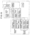
- Fig. 15 shows a simple block diagram of a driver circuit. All signal tuning operations are performed in response to a clock (shown in Fig. 15). Gate signal output timings of the lines, reset signals for the source electrodes, and recording and auxiliary signal output timings are controlled by this clock.
- the ionic localization state is stabilized when the FCL state is the full “black” state.
- this localization may be stabilized when the FCL state is a full “white” state.
- a waveform in Fig. 16(d) is continuously applied.
- the DC component source for maintaining the ionic localization in the "black” state is and this component is applied as the auxiliary signal.
- the "white” domain ratio is given as ⁇ a
- an auxiliary voltage having the following DC component superposing amount is applied (Figs. 16(a) to 16(d)): That is, when the present invention is applied to the active matrix driving, the auxiliary voltage signals are given as follows, as shown in Fig.
- the DC component value is always smaller than Vth.
- a good liquid crystal display As has been described above, there is provided a good liquid crystal display.
- a high-precision direct viewing flat display or a projection display can be arranged.
- a color filter on each pixel, or by using a plurality of liquid crystal elements of the driving method of the present invention so as to perform color light projection, a transmission or reflection type high-definition flat color television or projection color television can be arranged.
- the present invention is not limited to the driving techniques in the above embodiment.
- the present invention is widely applicable as optical elements consisting of liquid crystals having spontaneous polarization to perform stable gradation display.
- a liquid crystal apparatus including a liquid crystal panel having a pair of electrodes and a liquid crystal exhibiting spontaneous polarization and arranged between the pair of electrodes, first means for applying a gradation voltage signal corresponding to gradation information to the pair of electrodes, and second means for applying, a DC component serving as a reverse bias of an internal electric field generated upon application of the gradation voltage signal, to the liquid crystal during one vertical scanning period.
Abstract
Description
- The present invention relates to a liquid crystal apparatus exhibiting spontaneous polarization and, more particularly, to a liquid crystal apparatus using a ferroelectric liquid crystal (FLC).
- A ferroelectric liquid crystal (FLC) as a liquid crystal exhibiting the spontaneous polarization has received a great deal of attention in favor of advantages such as high-speed response and good memory characteristics and has been actively developed to obtain a light bulb and the like. Targets utilizing the above advantages are an optical shutter array, a high-definition display unit by simple matrix driving, a light bulb for high-density recording combined with a photoconductive body. In addition, the ferroelectric liquid crystal is expected to display a motion picture by active matrix driving using thin film transistors (TFTs). These characteristics are disclosed in U.S.P. No. 4,840,462, the Proceeding of the SID, Vol. 30/2, 1989 "Ferroelectric Liquid Crystal Video Display", and the like.
- In driving of the FLC, the following problems are posed generally or found to be caused as a result of experiments conducted by the present inventors.
- One of the problems is a decrease in response speed of the liquid crystal when a direct current (DC) component is continuously applied to the FLC for a long period of time due to the following reason. Localization of internal ions in the liquid crystal is assumed to be induced to form an electric field.
- To solve this problem, the present applicant made a proposal (Japanese Patent Application No. 2-69547) for canceling a DC component by an auxiliary pulse. In addition, since an FLC has spontaneous polarization, an electric field is formed by internal ions localized in correspondence with this spontaneous polarization, and a desired gradation image becomes unstable. It is found that hysteresis occurs in optical response to an external voltage value (applied voltage value).
- The phenomenon occurring upon application of a reset pulse and a write pulse continuously to the FLC at a drive frequency of about a television rate (60 Hz) will be described with reference to Figs. 20 to 22.
- In consideration of the problems found in the above experiments, in order to stably obtain a gradation image (gradation display) at a television rate in the FLC optical response, the present inventors have made further extensive studies in detail.
- It is an object of the present invention to provide a liquid crystal apparatus suitable for gradation display.
- It is another object of the present invention to provide a liquid crystal apparatus for realizing improved gradation display by using both an active matrix drive scheme using TFTs and a liquid crystal exhibiting spontaneous polarization, such as a ferroelectric liquid crystal.
- According to the first aspect of the present invention, there is provided a liquid crystal apparatus comprising a pair of electrodes, a liquid crystal panel having a liquid crystal arranged between the pair of electrodes and exhibiting spontaneous polarization, first means for applying a gradation voltage signal corresponding to gradation information to the pair of electrodes, and second means for applying, a DC component serving as a reverse bias for an internal electric field generated upon application of the gradation voltage signal, to the liquid crystal during one vertical scanning period.
- According to the second aspect of the present invention, there is provided a liquid crystal element comprising a liquid crystal exhibiting spontaneous polarization, a pair of electrode substrates for sandwiching the liquid crystal therebetween, and insulating layers formed between the liquid crystal and the pair of electrode substrates, wherein the following condition is established between a spontaneous polarization Ps value of the liquid crystal, an interelectrode composite capacitance Ci of the insulating layers, and a threshold voltage value Vth of an optical response of the liquid crystal in the liquid crystal element:

-
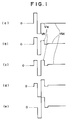
- Figs. 1(a) to 1(e) are waveform charts of drive signals used in the present invention;
- Fig. 2A is a sectional view of a cell used in the present invention;
- Fig. 2B is an equivalent circuit diagram of the cell;
- Figs. 3 to 5C are diagrams showing polarization states in the cell of the present invention;
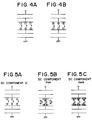
- Figs. 6A to 6C are waveform charts of drive signals used in the present invention;
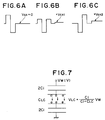
- Fig. 7 is an equivalent circuit diagram showing a polarization state in the cell used in the present invention;
- Fig. 8 is a waveform chart showing drive signals used in the cell of the present invention;
- Fig. 9 is an equivalent circuit diagram showing a polarization state in the cell used in the present invention;
- Figs. 10 and 11 are views showing changes in response time upon continuous application of a DC component of about 0.3 V as Vsx at a 44-Hz period;
- Figs. 12 and 13 are waveform charts showing drive signals used in the present invention;
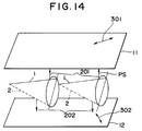
- Fig. 14 is a perspective view of the FLC;
- Fig. 15 is a block diagram of an apparatus according to the present invention;
- Fig. 16(a) to 16(d) are waveform charts of drive signals used in the present invention;
- Fig. 17 is a plan view of a panel;
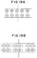
- Figs. 18A and 18B and Figs. 19A and 19B are views showing polarization states of the cell of the present invention;
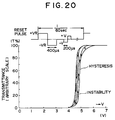
- Fig. 20 is a graph for explaining a V-T curve and hysteresis instability obtained upon continuous voltage application at a 60-Hz period;
- Fig. 21 is a graph for explaining instability exhibited upon continuous voltage application at a 44-Hz period;
- Fig. 22 is a graph for explaining a change in response deterioration over time upon continuous application of a 0.9 Va DC component at the 44-Hz period; and
- Fig. 23 is a sectional view of a cell of the present invention.
- A liquid crystal panel used in the present invention is a liquid crystal panel of an active matrix drive scheme, as shown in Fig. 17. The liquid crystal panel comprises switching elements (TFTs obtained by using thin film semiconductors such as amorphous silicon and polysilicon) arranged along a plurality of rows (scanning lines) and a plurality of columns (data lines), first wiring lines (gate lines) commonly connecting the first terminals (gates) of the switching elements in units of rows, second wiring lines (source lines) connecting the second terminals (sources) of the switching elements in units of columns, a plurality of pixel electrodes (transparent electrodes) connected in units of third terminals (drains) of the switching elements, counter electrodes (transparent electrodes) arranged to oppose the pixel electrodes, and a liquid crystal (chiral smectic C, H, I, G, F liquid crystal exhibiting ferroelectric properties) exhibiting spontaneous polarization and arranged between the plurality of pixel electrodes and the counter electrodes.
- The distance between each pixel electrode and the corresponding counter electrode is set to be a minimum distance (about 5 µm or less) capable of sufficiently suppressing formation of a helical structure of the chiral smectic liquid crystal. However, the formation of the helical structure need not be suppressed in the present invention.
- Thermal control may be performed during driving of the liquid crystal to maintain the liquid crystal within a desired temperature range.
- As shown in Figs. 1(a) to 1(e), after a reset voltage signal VR and a recording voltage signal VW which are applied to a pixel for a predetermined period of time required to cause an optical change of the pixel, an auxiliary voltage signal Vsx having a magnitude corresponding to that of the recording voltage signal VW is applied, thereby controlling an internal electric field to be described below.
- In order to describe the auxiliary voltage signal in more detail, the internal electric field generated by ionic localization caused by the DC component spontaneous polarization will be described below.
- Figs. 2A and 2B show a pseudo equivalent circuit model of an FLC element. Fig. 3 shows an ionic localization diagram obtained when an external DC component is applied for a long period of time. When a positive external DC component is applied, it is assumed that ionic localization indicated by ⊕ and ⊖ occurs inside the liquid crystal layer. At this time, if the upward direction (↑

- Figs. 4A and 4B show ionic localization by spontaneous polarization (PS) itself. When the direction of the spontaneous polarization (PS) is kept in the "black" (↑


- The function of the present invention will be described in more detail with reference to the waveforms of the drive signals in Figs. 1(a) to 1(e).
- Although the number of ions induced by spontaneous polarization is difficult to control, the DC component can be controlled by an external voltage applied to the liquid crystal. According to the present invention, the auxiliary voltage VS serves as a DC component, and the ionic localization is kept "constant" regardless of the state of the spontaneous polarization PS. The term "constant" indicates a total amount of ionic localization. The "constant" value may be a predetermined value or zero. However, the "constant" value need not always be zero.
- A method of adjusting the ionic localization to be "constant" will be described with reference to Figs. 5A to 5C. For a example, a total amount of ionic localization is apparently maintained to be an amount with which the "black" state as shown in Fig. 4A is kept set.
- The ionic localization sate of the "black" state shown in Fig. 5A is taken as an initial state. In this case, a drive signal having a waveform shown in Fig. 1(a) is applied to the liquid crystal in advance. In order to display the "black" state from this state, a drive signal having a waveform shown in Fig. 6A is applied to obtain the "black" state. At this time, the superposition amount of the DC component by the auxiliary voltage VSX may be zero. In order to display a gradation state, as shown in Fig. 5B, the ionic localization state to be obtained by this display is as shown in Fig. 18A. In order to keep the total ionic localization amount constant in the "black" display state, an auxiliary voltage +VSX1 shown in Fig. 6A is applied to add the ionic localization of Fig. 18B. In order to obtain a "white" state, as shown in Fig. 6C, an auxiliary voltage +VSX2 (Fig. 6C) is applied to maintain the state of Fig. 19A (i.e., the ionic localization state formed by this display) to the total amount obtained in the case of the "black" display.
- The numerical control of the auxiliary voltages VSX1 and VSX2 is appropriately performed in accordance with the magnitude of the instantaneous polarization PS and the ambient temperature. It is advantageous if the magnitude of the spontaneous polarization PS is set not so large (i.e., 10 nC/cm² or less, and preferably 5 nC/cm² or less) in the liquid crystal used in the present invention since then an excessive increase in the amplitude of the auxiliary voltage signal VSX can be suppressed. The numerical value for the amplitude of the signal VSX1 preferably falls within the following range:

(where Δa is the gradation at the end of application of the voltage VW and satisfiescondition 0 < Δa < 1, and Ci is the capacitance of the insulating layer)
The criterion for this numeric value will be described below with reference to Fig. 7. Fig. 7 shows a measurement of a divided voltage applied to a liquid crystal layer when a terminal voltage of a liquid crystal pixel is set at 0 V immediately after a gradation recording voltage VW is applied. At this time, the liquid crystal molecules are partially returned to the "black" direction and are set in the gradation state. If the ratio of the "white" state is defined as Δa, the divided voltage of the liquid crystal layer is given as follows:
Since a voltage which causes movement of ions in this gradation state is given by the above relation, if an external reverse voltage VSX of the voltage which causes this movement of ions is applied and the divided voltage of the liquid crystal
by the voltage VSX is set to equal to
movement of ions is assumed not to occur. Therefore, the following equation is established:
and the solution can be obtained as follows:
- For example, if PS and Ci are 5 nC/cm² and 20 µF/cm², respectively, the voltage VSX = about 0.5 V can be obtained even in the full "white" state.
- When the voltage VSX is applied within the range of 0 V to 0.5 V with the waveform shown in Fig. 8 in accordance with the gradation state, the initial ionic localization state can be maintained constant.
- When the voltage VSX corresponding to the gradation state of each frame is kept applied as a DC component until the next frame in image display repetition, ionic localization can be kept constant. Therefore, instability which may be caused by ionic localization can be eliminated.
- Second, since the DC component also serves as a "white" retention voltage of the liquid crystal, high-speed response of the liquid crystal can be obtained and can cope with the motion picture.
- Figs. 10 and 11 show an optical response test improved by the above driving method.
- As described above, in order to stabilize the ionic localization state caused by a display state, the peak value

of the auxiliary voltage is preferably stabilized. According to this driving method, the maximum value of the voltage VSX is preferably set as follows:
The present invention proposes the optical element on the basis of the findings that the above condition must be essentially satisfied to balance the ions. - As a condition of a liquid crystal element structure shown in Fig. 23, the effective magnitude of the spontaneous polarization PS of the liquid crystal used and the composite capacitance Ci of the alignment layers as important components constituting the element or an insulating layer portion including an additional insulating layer in the element must satisfy the above permanent relationship, thereby performing substantially stable gradation driving.
- From the qualitative viewpoint, the composite capacitance Ci is preferably set to be large, and the spontaneous polarization value PS of the liquid crystal used is preferably set to be small.
- In an experiment conducted by the present inventors, insulating layers formed to prevent electrical short-circuiting of the upper and lower electrodes of each cell are formed such that an oxide mixture (Ti-SiOX) of Ti (titanium) and Si (silicon) is coated on the electrodes and baked to obtain thin films each having a thickness of about 1,000 Å. A 200 Å thick polyimide alignment layer is formed on this insulating film and baked. The resultant structure is rubbed to maximize the composite capacitance Ci. In this case, the capacitance Ci can be about several 10 nF/cm². In order to further increase the capacitance Ci, the physical film thickness must be decreased, and a layer having a high dielectric constant is selected.
- The magnitude of the spontaneous polarization PS of the liquid crystal is a maximum of 10 nC/cm² when it is evaluated by a polarization reverse current. This magnitude is preferably 5 nC/cm² or less. As a result, the value 2PS/Ci is set to be about 0.5 V or less. In order to increase the value Vth, the viscosity of the liquid crystal is adjusted. However, it is generally disadvantageous to increase the drive voltage.
- In this case, the voltage Vth is defined as a DC application voltage limit with which an optical change is substantially not detected during a period of gradation display in driving the element.
- A driving method of the element will be described below.
- The above driving method cannot control each gradation level in formation of an image by a simple matrix. However, in principle, this driving method can be applied to an arrangement for driving pixels independently of each other as in driving of a single-bit optical shutter or a 7-segment display, or as in active matrix driving of TFTs (Thin Film Transistors).
- Actual drive waveforms in TFT active matrix driving will be described in detail below.
- Fig. 12 is a timing chart showing drive waveforms when the present invention is applied to active matrix driving.
- A reset signal VR for setting a pixel in the "black" state is applied, and a time voltage for sufficiently setting the pixel in the "black" state by utilizing the open characteristics of the TFT is also applied (Vr in Fig. 12). A recording voltage VW is applied, and this gradation level voltage VW is kept applied for a predetermined period of time in accordance with similar open characteristics. A ground signal VE is then applied to the pixel. During application of a ground voltage Ve, the gradation transmittance is changed but can be stabilized by the following auxiliary signal.
- The auxiliary voltage signal VSX is then applied to the pixel. This signal can be selected from VSX1 and VSX2 in accordance with a desired gradation display state. As indicated by the voltages VSX1 and VSX2 in the display frame serving as one vertical scanning period in the gradation transmitting state, the auxiliary voltage signal is applied as a voltage value containing an appropriate DC voltage. Note that when a sufficiently high voltage is applied as the reset voltage, the voltages VSX1 and VSX2 may be applied as values added with voltages for effecting the DC components corresponding to the gradation levels after the voltage difference between the voltages Vr and VW is compensated to be zero during the frame period.
- The target DC component value of this auxiliary voltage signal VSX is selected in accordance with the magnitude of the spontaneous polarization Ps of the liquid crystal used. The target magnitude of the DC component value is given as

in accordance with the ratio Δa of the "white" state when the maximum transmittance is defined as "1". For example, if Ps to 5 nC/cm², and the capacitance of the insulating layers constituting the liquid crystal cell is about 20 nF/cm², the voltage VW for recording the full "White" state is set to be about 0.5 V. In the gradation display state, a DC component of about 0.5 V or less is superposed on the auxiliary voltage signal. - The recording voltage VW or the recording voltage signal VW is a signal for determining the optical state of each pixel and represents a voltage signal (gradation voltage signal) corresponding to display brightness of the pixel. The auxiliary voltage VSX or the auxiliary voltage signal VSX is assumed to be a voltage for substantially stabilizing the gradation display state. This voltage signal is stabilized well at a DC voltage equal to or less than the optical threshold value Vth. In this case, the optical threshold value Vth is defined as a value with which an optical change is substantially not detected even if the threshold value Vth is kept applied throughout one frame.
- The absolute value of the auxiliary voltage signal VSX is preferably set to be about 1/50 to 1/5 that of the gradation voltage signal.
- Referring to Fig. 12, the application interval of the ground voltage Ve between the voltages VW and VSX is given to stabilize a reaction component as response of the liquid crystal molecules after the gradation voltage signal VW is applied. However, even if this application interval is not provided in this element, the driving effect is not impaired in this embodiment. In this case, the VSX value must be appropriately regulated in accordance with a drive waveform.
- If a change in state of the liquid crystal is assumed to occur by the application interval of the reset voltage signal Vr, the application intervals of the voltage signals VW and VE can be set equal to that of the reset voltage Vr.
- In order to effectively practice the above driving method, a recording period of each line is divided into at least four intervals (if the VE application interval is not provided, only three intervals are required; and the following description exemplifies a case wherein the VE application interval is provided). Referring to Fig. 12, the lower timing chart represents a case wherein the recording period A of the nth line is divided into four intervals. That is, the recording period A is divided into a division interval a for enabling a gate corresponding to a subsequent line a few lines after the current line to reset the pixels of the subsequent line, a division interval b for enabling a gate of the nth line to perform recording of the nth line itself, a division interval c for enabling a gate corresponding to a previous line a few lines before the current line to apply the ground voltage to the recorded pixels of the previous line, and a division interval d for enabling a gate corresponding to another previous line a few lines before the above previous line to apply an auxiliary voltage signal to the recorded pixels of this other previous line. Note that the division intervals a, b, c, and d in the recording period A of the nth line may have any one of the following orders: abcd, abdc, acdb, acbd, bacd, badc, bcad, bcda, bdac, bdca, cabd,....
- Fig. 12 shows optical states 101 to 104 of a liquid crystal pixel of the nth line. These states are enlarged in Fig. 13.
- Fig. 14 is a view showing an FLC sandwiched between an
upper electrode substrate 11 having a TFT active matrix and a lower substrate with its entire surface serving as an electrode. - In principle, when the direction of the spontaneous polarization PS is upward 201, the major axis of each FLC molecule is given as a direction indicated by a
solid line 1; and when the direction of the spontaneous polarization PS is downward 202, the major axis of each FLC molecule is given as a direction indicated by a dottedline 2. When the reset voltage Vr shown in Fig. 20 is applied to keep the upper electrode in a negative state, the spontaneous polarization is ideally directed in theupward direction 201 during this interval. When one ofpolarizing plates solid line 1, the pixel is set in the "black" state. Therefore, full "black" states 101 and 103 in Fig. 12 can be obtained. - When the gradation voltage signal as the recording voltage signal VW has a magnitude larger than the reverse threshold value Vth of the liquid crystal, a "white" domain is formed. However, if VW is less than Vth, a reset "black" state is maintained. When the ground voltage signal VE is enabled to apply the ground voltage Ve, some molecules which are not latched to the "white" state tend to react, but the state is transited to the gradation display state (103 in Fig. 12) corresponding to the gradation voltage VW. Thereafter, when the auxiliary voltage signal VSX corresponding to the voltage VW is applied, the gradation state is maintained, and variations in ionic localization described above can be prevented. As a result, since the variations in ionic polarization are eliminated in each frame, no undesirable change in transmittance occurs. Therefore, a stable image display operation can be performed.
- In a so-called high-vision compatible television display, when about 1,000 scanning lines are interlaced-scanned at 30 or 60 Hz, each frame is driven for about 33 msec. For this reason, a recording period assigned to each line is about 33 µsec per frame. The recording period of 33 µsec for applying a recording voltage every nth line according to the present invention is divided into four intervals (i.e., each interval is about 8 µsec or less). For example, these four intervals consist of an interval for applying the VR pulse for resetting a line pixel applied with the recording voltage (VW) six lines after the current line (= S₃), a recording pulse interval for applying the voltage VW to the pixel of the nth line, a ground signal interval for applying the ground voltage VE to a line pixel having been applied with the voltage VW six lines before the current line (= S₂), and an interval for applying the auxiliary voltage signal VSX to a line pixel having been applied with the
V W 12 lines before the current line (= S₁). A total time for applying the respective voltages becomes about 198 µsec (= about 33 µsec x 6). A satisfactory image display could be obtained by the material used by the present inventor at maximum VR and VW voltages of about 7 V. In addition, the DC component was superposed on the auxiliary voltage VSX by a voltage equal to or less than the threshold value Vth corresponding to the gradation level to stabilize the gradation display state. - The driving method shown in Fig. 12 will be described in more detail with reference to Fig. 13.
- The pulse peak value of the auxiliary voltage signal VSX can be determined as follows.
- Assume that the peak value VR of the reset voltage Vr in the ideal voltage waveform during the reset signal interval a is -V₀, and that the peak value VW of the recording voltage VW during the recording signal interval b is +V₀. If the times for applying these voltages are equal to each other, a peak value VS0 of the auxiliary voltage signal VSX during the auxiliary voltage signal interval d is set at 0.5 V if Ps to 5 nC/cm² and Ci to 20 nF/cm², in accordance with calculation

(interval 401). - On the other hand, when gradation levels are assigned to the recording signal as indicated by
intervals 
When the DC components by the voltages Vr and VW are set to zero, and a voltage value corresponding to
is added to each zero DC component value, so that the peak values of the auxiliary voltage signals are defined with respect to gradation values (based on transmittances at the end of ground voltage application period) Δa₁, Δa₂, and Δa₃ as follows:
- If the intervals S₂, S₃, and (S₄ - S₃) are different from each other, the voltage VS1ʼ can be rewritten as follows:

- For example, assume that the spontaneous polarization PS of the FLC used equals 5 nm/cm², the capacitance Ci is 20 nF/cm², the voltage VW is -7 V, and a 60% transmittance is obtained at V₁ of 5.5 V. If the S₂ = S₃ = (S₄ - S₃) = 6, then the following equation is obtained:

and therefore,

- The auxiliary voltage signal VSX may be calculated in accordance with the analog recording signal voltage VW on the spot, or may be automatically output from a prestored table T (VW and VSX) if the recording signal VW is a digital signal.
- The driving method of the present invention can be easily realized by arranging a frame memory or a line memory of at least S₄ lines in principle.
- That is, since a delay time of S₄ = 12 lines is present between generation of the recording signal and generation of the auxiliary signal, information of S₄ = 12 lines must be stored for generation of recording signals for other lines during this period.
- Fig. 15 shows a simple block diagram of a driver circuit. All signal tuning operations are performed in response to a clock (shown in Fig. 15). Gate signal output timings of the lines, reset signals for the source electrodes, and recording and auxiliary signal output timings are controlled by this clock.
- It is readily understood that a good effect can be obtained by a combination of a liquid crystal having spontaneous polarization and an active matrix element in order to apply the auxiliary voltage.
- In the above description, the ionic localization state is stabilized when the FCL state is the full "black" state. However, this localization may be stabilized when the FCL state is a full "white" state.
- In this case, ionic localization in the initial "white" state is caused to occur to start the operation. According to this method, a waveform in Fig. 16(d) is continuously applied. The DC component source for maintaining the ionic localization in the "black" state is

and this component is applied as the auxiliary signal. If the "white" domain ratio is given as Δa, in order to maintain the ionic localization amount in the "white" state with respect to the remaining black domain ratio (1 - Δa), an auxiliary voltage having the following DC component superposing amount is applied (Figs. 16(a) to 16(d)):
That is, when the present invention is applied to the active matrix driving, the auxiliary voltage signals are given as follows, as shown in Fig. 21:
In this case, the correspondence between the recording voltage values V₁, V₂, and V₃ (Fig. 13) and the gradation values Δa₁, Δa₂, and Δa₃ is different from the case wherein the ionic localization is stabilized in the "black" state. A lower voltage is selected as the voltage VW to obtain good gradation display as in the above embodiment. - When the stabilized gradation display is achieved, the DC component value

is always smaller than Vth. - According to the optical modulation element, as has been described above, there is provided a good liquid crystal display. A high-precision direct viewing flat display or a projection display can be arranged. As a matter of course, by arranging a color filter on each pixel, or by using a plurality of liquid crystal elements of the driving method of the present invention so as to perform color light projection, a transmission or reflection type high-definition flat color television or projection color television can be arranged.
- The present invention is not limited to the driving techniques in the above embodiment. The present invention is widely applicable as optical elements consisting of liquid crystals having spontaneous polarization to perform stable gradation display.
- Disclosed is a liquid crystal apparatus including a liquid crystal panel having a pair of electrodes and a liquid crystal exhibiting spontaneous polarization and arranged between the pair of electrodes, first means for applying a gradation voltage signal corresponding to gradation information to the pair of electrodes, and second means for applying, a DC component serving as a reverse bias of an internal electric field generated upon application of the gradation voltage signal, to the liquid crystal during one vertical scanning period.
Claims (30)
- A liquid crystal apparatus comprising a liquid crystal panel having a pair of electrodes and a liquid crystal exhibiting spontaneous polarization and arranged between said pair of electrodes, first means for applying a gradation voltage signal corresponding to gradation information to said pair of electrodes, and second means for applying, a DC component serving as a reverse bias of an internal electric field generated upon application of the gradation voltage signal, to said liquid crystal during one vertical scanning period.
- An apparatus according to claim 1, wherein said liquid crystal essentially consists of a ferroelectric liquid crystal.
- An apparatus according to claim 1, wherein said one vertical scanning period is one frame scanning period.
- An apparatus according to claim 1, wherein a value of the DC component is within a range of 1/50 to 1/5 of the gradation voltage signal.
- A liquid crystal apparatus comprising:a. a liquid crystal panel having switching elements arranged along a plurality of rows and a plurality of columns, first wiring lines commonly connecting first terminals of said switching elements in units of rows, second wiring lines commonly connecting second terminals of said switching elements in units of columns, a plurality of pixel electrodes connected in units of third terminals of said switching elements, counter electrodes opposite to said pixel electrodes, and a liquid crystal exhibiting spontaneous polarization and sandwiched between said plurality of pixel electrodes and said counter electrodes;b. first means for applying scanning pulses to said first wiring lines; andc. second means for applying a gradation voltage signal corresponding to gradation information to said second wiring lines and for applying an auxiliary voltage signal to said second wiring lines so that a DC component serving as a reverse bias for an internal electric field generated upon application of the gradation voltage signal is applied to said liquid crystal during one vertical scanning period.
- An apparatus according to claim 5, wherein said liquid crystal essentially consists of a ferroelectric liquid crystal.
- An apparatus according to claim 5, wherein said one vertical scanning period is one frame scanning period.
- An apparatus according to claim 5, wherein a value of the DC component is within a range of 1/50 to 1/5 of the gradation voltage signal.
- A liquid crystal apparatus comprising:a. a liquid crystal panel having switching elements arranged along a plurality of rows and a plurality of columns, first wiring lines commonly connecting first terminals of said switching elements in units of rows, second wiring lines commonly connecting second terminals of said switching elements in units of columns, a plurality of pixel electrodes connected in units of third terminals of said switching elements, counter electrodes opposite to said pixel electrodes, and a liquid crystal exhibiting spontaneous polarization and sandwiched between said plurality of pixel electrodes and said counter electrodes;b. first means for applying scanning pulses to said first wiring lines; andc. second means for applying a voltage signal corresponding to gradation information to said second wiring lines after a reset voltage signal is applied and for applying an auxiliary voltage signal to said second wiring lines such that a DC component serving as a reverse bias for an internal electric field generated upon application of the gradation voltage signal is applied to said liquid crystal during one vertical scanning period.
- An apparatus according to claim 9, wherein said liquid crystal essentially consists of a ferroelectric liquid crystal.
- An apparatus according to claim 9, wherein said one vertical scanning period is one frame scanning period.
- An apparatus according to claim 9, wherein a value of the DC component is within a range of 1/50 to 1/5 of the gradation voltage signal.
- An apparatus according to claim 9, further comprising means for applying, prior to application of the reset voltage signal, a voltage signal given such that a difference between an absolute value of the reset voltage signal and an absolute value of the gradation voltage signal becomes zero.
- An apparatus according to claim 9, further comprising means for applying a zero voltage during a period between the auxiliary voltage signal and the gradation voltage signal.
- A liquid crystal element comprising a liquid crystal exhibiting spontaneous polarization, a pair of electrode substrates for sandwiching said liquid crystal therebetween, and insulating layers formed between said electrode substrates and said liquid crystal, wherein a spontaneous polarization PS value of said liquid crystal, an interelectrode composite capacitance Ci of said insulating layers, and a voltage threshold value Vth of optical response of said liquid crystal in said liquid crystal element satisfy the following condition:

- An element according to claim 15, wherein said liquid crystal essentially consists of a ferroelectric liquid crystal.
- A liquid crystal apparatus comprising:
a liquid crystal element having a liquid crystal having spontaneous polarization, a pair of electrode substrates for sandwiching said liquid crystal therebetween, and insulating layers formed between said electrode substrates and said liquid crystal, wherein a spontaneous polarization PS value of said liquid crystal, an interelectrode composite capacitance Ci of said insulating layers, and a voltage threshold value Vth of optical response of said liquid crystal in said liquid crystal element satisfy the following condition:
second means for applying, a DC component serving as a reverse bias of an internal electric field generated upon application of the gradation voltage signal, to said liquid crystal during one vertical scanning period. - An apparatus according to claim 17, wherein said liquid crystal essentially consists of a ferroelectric liquid crystal.
- An apparatus according to claim 17, wherein said one vertical scanning period is one frame scanning period.
- An apparatus according to claim 17, wherein a value of the DC component is within a range of 1/50 to 1/5 of the gradation voltage signal.
- A liquid crystal apparatus comprising:a. a liquid crystal element having switching elements arranged along a plurality of rows and a plurality of columns, first wiring lines commonly connecting first terminals of said switching elements in units of rows, second wiring lines commonly connecting second terminals of said switching elements in units of columns, a plurality of pixel electrodes connected in units of third terminals of said switching elements, counter electrodes opposite to said pixel electrodes, a liquid crystal exhibiting spontaneous polarization PS and sandwiched between said plurality of pixel electrodes and said counter electrodes, and an insulating member formed on at least one of said pixel and counter electrodes, a voltage threshold value Vth of optical response of said liquid crystal and an interelectrode capacitance Ci of said insulating member satisfying the following condition:
 b. first means for applying scanning pulses to said first wiring lines; andc. second means for applying a gradation voltage signal corresponding to gradation information to said second wiring lines and for applying an auxiliary voltage signal to said second wiring lines so that a DC component serving as a reverse bias for an internal electric field generated upon application of the gradation voltage signal is applied to said liquid crystal during one vertical scanning period.
 - An apparatus according to claim 21, wherein said liquid crystal essentially consists of a ferroelectric liquid crystal.
- An apparatus according to claim 21, wherein said one vertical scanning period is one frame scanning period.
- An apparatus according to claim 21, wherein a value of the DC component is within a range of 1/50 to 1/5 of the gradation voltage signal.
- A liquid crystal apparatus comprising:a. a liquid crystal element having switching elements arranged along a plurality of rows and a plurality of columns, first wiring lines commonly connecting first terminals of said switching elements in units of rows, second wiring lines commonly connecting second terminals of said switching elements in units of columns, a plurality of pixel electrodes connected in units of third terminals of said switching elements, counter electrodes opposite to said pixel electrodes, a liquid crystal exhibiting spontaneous polarization PS and sandwiched between said plurality of pixel electrodes and said counter electrodes, and an insulating member formed on at least one of said pixel and counter electrodes, a voltage threshold value Vth of liquid crystal of said optical response and an interelectrode capacitance Ci of said insulating member satisfying the following condition:
 b. first means for applying scanning pulses to said first wiring lines; andc. second means for applying a voltage signal corresponding to gradation information to said second wiring lines after a reset voltage signal is applied and for applying an auxiliary voltage signal to said second wiring lines such that a DC component serving as a reverse bias for an internal electric field generated upon application of the gradation voltage signal is applied to said liquid crystal during one vertical scanning period.
 - An apparatus according to claim 25, wherein said liquid crystal essentially consists of a ferroelectric liquid crystal.
- An apparatus according to claim 25, wherein said one vertical scanning period is one frame scanning period.
- An apparatus according to claim 25, wherein a value of the DC component is within a range of 1/50 to 1/5 of the gradation voltage signal.
- An apparatus according to claim 25, further comprising means for applying, prior to application of the reset voltage signal, a voltage signal given such that a difference between an absolute value of the reset voltage signal and an absolute value of the gradation voltage signal becomes zero.
- An apparatus according to claim 25, further comprising means for applying a zero voltage during a period between the auxiliary voltage signal and the gradation voltage signal.
Priority Applications (1)
| Application Number | Priority Date | Filing Date | Title |
|---|---|---|---|
| EP96102488A EP0717305B1 (en) | 1990-08-22 | 1991-08-21 | Liquid crystal apparatus |
Applications Claiming Priority (7)
| Application Number | Priority Date | Filing Date | Title |
|---|---|---|---|
| JP221709/90 | 1990-08-22 | ||
| JP22170990 | 1990-08-22 | ||
| JP22171090 | 1990-08-22 | ||
| JP221710/90 | 1990-08-22 | ||
| JP03192048A JP3143497B2 (en) | 1990-08-22 | 1991-07-31 | Liquid crystal device |
| JP192048/91 | 1991-07-31 | ||
| US07/746,338 US5396352A (en) | 1990-08-22 | 1991-08-16 | Liquid crystal apparatus with gradation information signals and DC bias |
Related Child Applications (2)
| Application Number | Title | Priority Date | Filing Date |
|---|---|---|---|
| EP96102488.2 Division-Into | 1991-08-21 | ||
| EP96102488A Division EP0717305B1 (en) | 1990-08-22 | 1991-08-21 | Liquid crystal apparatus |
Publications (3)
| Publication Number | Publication Date |
|---|---|
| EP0473058A2 true EP0473058A2 (en) | 1992-03-04 |
| EP0473058A3 EP0473058A3 (en) | 1993-04-07 |
| EP0473058B1 EP0473058B1 (en) | 1997-03-19 |
Family
ID=27475569
Family Applications (1)
| Application Number | Title | Priority Date | Filing Date |
|---|---|---|---|
| EP91114021A Expired - Lifetime EP0473058B1 (en) | 1990-08-22 | 1991-08-21 | Liquid crystal apparatus |
Country Status (4)
| Country | Link |
|---|---|
| US (2) | US5396352A (en) |
| EP (1) | EP0473058B1 (en) |
| JP (1) | JP3143497B2 (en) |
| CA (1) | CA2049624C (en) |
Cited By (1)
| Publication number | Priority date | Publication date | Assignee | Title |
|---|---|---|---|---|
| EP0735407A2 (en) * | 1995-03-28 | 1996-10-02 | Dai Nippon Printing Co., Ltd. | Method and apparatus for recording a photographic image on liquid crystal recording medium |
Families Citing this family (36)
| Publication number | Priority date | Publication date | Assignee | Title |
|---|---|---|---|---|
| JP2994814B2 (en) * | 1990-11-09 | 1999-12-27 | キヤノン株式会社 | Liquid crystal device |
| JP2826776B2 (en) * | 1991-02-20 | 1998-11-18 | キヤノン株式会社 | Ferroelectric liquid crystal device |
| US5592190A (en) * | 1993-04-28 | 1997-01-07 | Canon Kabushiki Kaisha | Liquid crystal display apparatus and drive method |
| US5798746A (en) * | 1993-12-27 | 1998-08-25 | Semiconductor Energy Laboratory Co., Ltd. | Liquid crystal display device |
| GB2295045B (en) * | 1994-11-08 | 1998-07-15 | Citizen Watch Co Ltd | A liquid crystal display device and a method of driving the same |
| JPH11326957A (en) * | 1998-03-20 | 1999-11-26 | Toshiba Corp | Liquid crystal display device |
| US6496170B1 (en) | 1998-04-30 | 2002-12-17 | Canon Kabushiki Kaisha | Liquid crystal apparatus |
| EP1043618A4 (en) * | 1998-10-22 | 2005-08-31 | Citizen Watch Co Ltd | Ferroelectric liquid crystal display, and its driving method |
| TW484117B (en) | 1999-11-08 | 2002-04-21 | Semiconductor Energy Lab | Electronic device |
| JP3918399B2 (en) | 2000-04-28 | 2007-05-23 | 富士通株式会社 | Liquid crystal element |
| JP2001337311A (en) * | 2000-05-29 | 2001-12-07 | Sony Corp | Method for driving liquid crystal display element |
| US6992652B2 (en) | 2000-08-08 | 2006-01-31 | Semiconductor Energy Laboratory Co., Ltd. | Liquid crystal display device and driving method thereof |
| TW522374B (en) * | 2000-08-08 | 2003-03-01 | Semiconductor Energy Lab | Electro-optical device and driving method of the same |
| TW518552B (en) | 2000-08-18 | 2003-01-21 | Semiconductor Energy Lab | Liquid crystal display device, method of driving the same, and method of driving a portable information device having the liquid crystal display device |
| US6987496B2 (en) * | 2000-08-18 | 2006-01-17 | Semiconductor Energy Laboratory Co., Ltd. | Electronic device and method of driving the same |
| US7180496B2 (en) * | 2000-08-18 | 2007-02-20 | Semiconductor Energy Laboratory Co., Ltd. | Liquid crystal display device and method of driving the same |
| TW514854B (en) | 2000-08-23 | 2002-12-21 | Semiconductor Energy Lab | Portable information apparatus and method of driving the same |
| JP4014831B2 (en) * | 2000-09-04 | 2007-11-28 | 株式会社半導体エネルギー研究所 | EL display device and driving method thereof |
| US6774876B2 (en) | 2000-10-02 | 2004-08-10 | Semiconductor Energy Laboratory Co., Ltd. | Self light emitting device and driving method thereof |
| US7184014B2 (en) | 2000-10-05 | 2007-02-27 | Semiconductor Energy Laboratory Co., Ltd. | Liquid crystal display device |
| EP1331507A4 (en) * | 2000-10-25 | 2008-04-16 | Toshiba Matsushita Display Tec | Liquid crystal display drive method and liquid crystal display |
| US6747623B2 (en) * | 2001-02-09 | 2004-06-08 | Semiconductor Energy Laboratory Co., Ltd. | Liquid crystal display device and method of driving the same |
| JP2003114646A (en) * | 2001-08-03 | 2003-04-18 | Semiconductor Energy Lab Co Ltd | Display device and its driving method |
| US7508479B2 (en) * | 2001-11-15 | 2009-03-24 | Samsung Electronics Co., Ltd. | Liquid crystal display |
| TWI273539B (en) | 2001-11-29 | 2007-02-11 | Semiconductor Energy Lab | Display device and display system using the same |
| JP3913534B2 (en) * | 2001-11-30 | 2007-05-09 | 株式会社半導体エネルギー研究所 | Display device and display system using the same |
| US6982727B2 (en) * | 2002-07-23 | 2006-01-03 | Broadcom Corporation | System and method for providing graphics using graphical engine |
| JP2005275315A (en) * | 2004-03-26 | 2005-10-06 | Semiconductor Energy Lab Co Ltd | Display device, driving method therefor, and electronic equipment using the same |
| US7502040B2 (en) * | 2004-12-06 | 2009-03-10 | Semiconductor Energy Laboratory Co., Ltd. | Display device, driving method thereof and electronic appliance |
| US20060139265A1 (en) * | 2004-12-28 | 2006-06-29 | Semiconductor Energy Laboratory Co., Ltd. | Driving method of display device |
| US20060158399A1 (en) | 2005-01-14 | 2006-07-20 | Semiconductor Energy Laboratory Co., Ltd. | Driving method of display device |
| US7719526B2 (en) | 2005-04-14 | 2010-05-18 | Semiconductor Energy Laboratory Co., Ltd. | Display device, and driving method and electronic apparatus of the display device |
| US8633919B2 (en) * | 2005-04-14 | 2014-01-21 | Semiconductor Energy Laboratory Co., Ltd. | Display device, driving method of the display device, and electronic device |
| EP1720148A3 (en) | 2005-05-02 | 2007-09-05 | Semiconductor Energy Laboratory Co., Ltd. | Display device and gray scale driving method with subframes thereof |
| KR101404582B1 (en) * | 2006-01-20 | 2014-06-09 | 가부시키가이샤 한도오따이 에네루기 켄큐쇼 | Driving method of display device |
| WO2013172220A1 (en) | 2012-05-18 | 2013-11-21 | Semiconductor Energy Laboratory Co., Ltd. | Pixel circuit, display device, and electronic device |
Citations (2)
| Publication number | Priority date | Publication date | Assignee | Title |
|---|---|---|---|---|
| EP0284134A1 (en) * | 1987-03-17 | 1988-09-28 | Koninklijke Philips Electronics N.V. | Method of driving a liquid crystal display device and associated display device |
| EP0367531A2 (en) * | 1988-11-01 | 1990-05-09 | Sharp Kabushiki Kaisha | Method of driving ferroelectric liquid crystal display panel |
Family Cites Families (10)
| Publication number | Priority date | Publication date | Assignee | Title |
|---|---|---|---|---|
| JPS6232424A (en) * | 1985-08-05 | 1987-02-12 | Canon Inc | Method for driving liquid crystal element |
| US4770502A (en) * | 1986-01-10 | 1988-09-13 | Hitachi, Ltd. | Ferroelectric liquid crystal matrix driving apparatus and method |
| ATE131290T1 (en) * | 1987-06-12 | 1995-12-15 | Canon Kk | DEVICE COMPRISING A FERROELECTRIC LIQUID CRYSTAL. |
| JPH078581B2 (en) * | 1987-09-14 | 1995-02-01 | 株式会社日立製作所 | Liquid crystal optical switch driving method |
| US5136408A (en) * | 1988-06-01 | 1992-08-04 | Canon Kabushiki Kaisha | Liquid crystal apparatus and driving method therefor |
| DE3824455A1 (en) * | 1988-07-19 | 1990-01-25 | Bayer Ag | THERMOPLASTIC MOLDS FROM POLYAMIDES AND RESIN COPOLYMERS WITH (METH) ACRYLAMIDE, METHOD FOR THEIR PRODUCTION AND THEIR USE |
| JP2655719B2 (en) * | 1989-03-20 | 1997-09-24 | 富士通株式会社 | Liquid crystal display device |
| GB2233106B (en) * | 1989-05-23 | 1993-08-25 | Citizen Watch Co Ltd | Ferroelectric liquid crystal element and method of driving the same |
| JP2769879B2 (en) * | 1989-09-29 | 1998-06-25 | キヤノン株式会社 | Chiral smectic liquid crystal device |
| US5227900A (en) * | 1990-03-20 | 1993-07-13 | Canon Kabushiki Kaisha | Method of driving ferroelectric liquid crystal element |
-
1991
- 1991-07-31 JP JP03192048A patent/JP3143497B2/en not_active Expired - Fee Related
- 1991-08-16 US US07/746,338 patent/US5396352A/en not_active Expired - Lifetime
- 1991-08-21 CA CA002049624A patent/CA2049624C/en not_active Expired - Fee Related
- 1991-08-21 EP EP91114021A patent/EP0473058B1/en not_active Expired - Lifetime
-
1994
- 1994-10-11 US US08/320,526 patent/US5479283A/en not_active Expired - Lifetime
Patent Citations (2)
| Publication number | Priority date | Publication date | Assignee | Title |
|---|---|---|---|---|
| EP0284134A1 (en) * | 1987-03-17 | 1988-09-28 | Koninklijke Philips Electronics N.V. | Method of driving a liquid crystal display device and associated display device |
| EP0367531A2 (en) * | 1988-11-01 | 1990-05-09 | Sharp Kabushiki Kaisha | Method of driving ferroelectric liquid crystal display panel |
Cited By (2)
| Publication number | Priority date | Publication date | Assignee | Title |
|---|---|---|---|---|
| EP0735407A2 (en) * | 1995-03-28 | 1996-10-02 | Dai Nippon Printing Co., Ltd. | Method and apparatus for recording a photographic image on liquid crystal recording medium |
| EP0735407A3 (en) * | 1995-03-28 | 1997-04-23 | Dainippon Printing Co Ltd | Method and apparatus for recording a photographic image on liquid crystal recording medium |
Also Published As
| Publication number | Publication date |
|---|---|
| CA2049624A1 (en) | 1992-02-23 |
| CA2049624C (en) | 1995-09-05 |
| EP0473058B1 (en) | 1997-03-19 |
| JPH052376A (en) | 1993-01-08 |
| JP3143497B2 (en) | 2001-03-07 |
| EP0473058A3 (en) | 1993-04-07 |
| US5479283A (en) | 1995-12-26 |
| US5396352A (en) | 1995-03-07 |
Similar Documents
| Publication | Publication Date | Title |
|---|---|---|
| EP0473058B1 (en) | Liquid crystal apparatus | |
| US5689320A (en) | Liquid crystal display apparatus having a film layer including polyaniline | |
| US5905484A (en) | Liquid crystal display device with control circuit | |
| EP0510606B1 (en) | Liquid crystal display apparatus | |
| EP0724759B1 (en) | Acive matrix liquid crystal display | |
| US5490000A (en) | Deformed helix ferroelectric liquid crystal display device and method of driving | |
| GB2324899A (en) | Active matrix display | |
| US5920301A (en) | Liquid crystal display apparatus using liquid crystal having ferroelectric phase and method of driving liquid crystal display device using liquid crystal having ferroelectric phase | |
| EP0448105B1 (en) | Method and apparatus for driving active matrix liquid crystal device | |
| US6191771B1 (en) | Liquid crystal display | |
| US6169531B1 (en) | Liquid-crystal control circuit display device with selection signal | |
| US5973657A (en) | Liquid crystal display apparatus | |
| EP0717305B1 (en) | Liquid crystal apparatus | |
| EP0526713A2 (en) | Liquid crystal display with active matrix | |
| US6069602A (en) | Liquid crystal display device, liquid crystal display apparatus and liquid crystal driving method | |
| JPH0764055A (en) | Ferroelectric liquid crystal display device and method for driving ferroelectric liquid crystal display element | |
| US20010045933A1 (en) | Liquid crystal optical apparatus | |
| JP2678591B2 (en) | Driving method of liquid crystal display device | |
| EP0686956A2 (en) | Liquid crystal display apparatus using liquid crystal having ferroelectric phase and method of driving liquid crystal display device using liquid crystal having ferroelectric phase | |
| JPH0815671A (en) | Liquid crystal display device and method of driving it | |
| CA2153707C (en) | Liquid crystal apparatus | |
| JP2933703B2 (en) | Liquid crystal device and driving method thereof | |
| JPH11231286A (en) | Driving method for antiferroelectric liquid crystal display element | |
| JP2727131B2 (en) | Driving method of active matrix liquid crystal device | |
| GB2205984A (en) | Electro-optical apparatus |
Legal Events
| Date | Code | Title | Description |
|---|---|---|---|
| PUAI | Public reference made under article 153(3) epc to a published international application that has entered the european phase |
Free format text: ORIGINAL CODE: 0009012 |
|
| AK | Designated contracting states |
Kind code of ref document: A2 Designated state(s): AT BE CH DE DK ES FR GB GR IT LI LU NL SE |
|
| PUAL | Search report despatched |
Free format text: ORIGINAL CODE: 0009013 |
|
| AK | Designated contracting states |
Kind code of ref document: A3 Designated state(s): AT BE CH DE DK ES FR GB GR IT LI LU NL SE |
|
| 17P | Request for examination filed |
Effective date: 19930824 |
|
| 17Q | First examination report despatched |
Effective date: 19941212 |
|
| GRAG | Despatch of communication of intention to grant |
Free format text: ORIGINAL CODE: EPIDOS AGRA |
|
| GRAH | Despatch of communication of intention to grant a patent |
Free format text: ORIGINAL CODE: EPIDOS IGRA |
|
| GRAH | Despatch of communication of intention to grant a patent |
Free format text: ORIGINAL CODE: EPIDOS IGRA |
|
| GRAA | (expected) grant |
Free format text: ORIGINAL CODE: 0009210 |
|
| AK | Designated contracting states |
Kind code of ref document: B1 Designated state(s): AT BE CH DE DK ES FR GB GR IT LI LU NL SE |
|
| DX | Miscellaneous (deleted) | ||
| PG25 | Lapsed in a contracting state [announced via postgrant information from national office to epo] |
Ref country code: LI Effective date: 19970319 Ref country code: GR Free format text: LAPSE BECAUSE OF FAILURE TO SUBMIT A TRANSLATION OF THE DESCRIPTION OR TO PAY THE FEE WITHIN THE PRESCRIBED TIME-LIMIT Effective date: 19970319 Ref country code: DK Effective date: 19970319 Ref country code: CH Effective date: 19970319 Ref country code: BE Effective date: 19970319 Ref country code: AT Effective date: 19970319 |
|
| REF | Corresponds to: |
Ref document number: 150570 Country of ref document: AT Date of ref document: 19970415 Kind code of ref document: T |
|
| REG | Reference to a national code |
Ref country code: CH Ref legal event code: EP |
|
| REF | Corresponds to: |
Ref document number: 69125228 Country of ref document: DE Date of ref document: 19970424 |
|
| REG | Reference to a national code |
Ref country code: ES Ref legal event code: FG2A Ref document number: 2098286 Country of ref document: ES Kind code of ref document: T3 |
|
| ET | Fr: translation filed | ||
| ITF | It: translation for a ep patent filed |
Owner name: SOCIETA' ITALIANA BREVETTI S.P.A. |
|
| PG25 | Lapsed in a contracting state [announced via postgrant information from national office to epo] |
Ref country code: LU Free format text: LAPSE BECAUSE OF NON-PAYMENT OF DUE FEES Effective date: 19970821 |
|
| REG | Reference to a national code |
Ref country code: CH Ref legal event code: PL |
|
| PLBE | No opposition filed within time limit |
Free format text: ORIGINAL CODE: 0009261 |
|
| STAA | Information on the status of an ep patent application or granted ep patent |
Free format text: STATUS: NO OPPOSITION FILED WITHIN TIME LIMIT |
|
| 26N | No opposition filed | ||
| REG | Reference to a national code |
Ref country code: GB Ref legal event code: IF02 |
|
| PGFP | Annual fee paid to national office [announced via postgrant information from national office to epo] |
Ref country code: DE Payment date: 20020829 Year of fee payment: 12 |
|
| PGFP | Annual fee paid to national office [announced via postgrant information from national office to epo] |
Ref country code: SE Payment date: 20030806 Year of fee payment: 13 |
|
| PGFP | Annual fee paid to national office [announced via postgrant information from national office to epo] |
Ref country code: FR Payment date: 20030808 Year of fee payment: 13 |
|
| PGFP | Annual fee paid to national office [announced via postgrant information from national office to epo] |
Ref country code: GB Payment date: 20030820 Year of fee payment: 13 |
|
| PGFP | Annual fee paid to national office [announced via postgrant information from national office to epo] |
Ref country code: NL Payment date: 20030831 Year of fee payment: 13 |
|
| PGFP | Annual fee paid to national office [announced via postgrant information from national office to epo] |
Ref country code: ES Payment date: 20030926 Year of fee payment: 13 |
|
| PG25 | Lapsed in a contracting state [announced via postgrant information from national office to epo] |
Ref country code: DE Free format text: LAPSE BECAUSE OF NON-PAYMENT OF DUE FEES Effective date: 20040302 |
|
| PG25 | Lapsed in a contracting state [announced via postgrant information from national office to epo] |
Ref country code: GB Free format text: LAPSE BECAUSE OF NON-PAYMENT OF DUE FEES Effective date: 20040821 |
|
| PG25 | Lapsed in a contracting state [announced via postgrant information from national office to epo] |
Ref country code: SE Free format text: LAPSE BECAUSE OF NON-PAYMENT OF DUE FEES Effective date: 20040822 |
|
| PG25 | Lapsed in a contracting state [announced via postgrant information from national office to epo] |
Ref country code: ES Free format text: LAPSE BECAUSE OF NON-PAYMENT OF DUE FEES Effective date: 20040823 |
|
| PG25 | Lapsed in a contracting state [announced via postgrant information from national office to epo] |
Ref country code: NL Free format text: LAPSE BECAUSE OF NON-PAYMENT OF DUE FEES Effective date: 20050301 |
|
| EUG | Se: european patent has lapsed | ||
| GBPC | Gb: european patent ceased through non-payment of renewal fee |
Effective date: 20040821 |
|
| PG25 | Lapsed in a contracting state [announced via postgrant information from national office to epo] |
Ref country code: FR Free format text: LAPSE BECAUSE OF NON-PAYMENT OF DUE FEES Effective date: 20050429 |
|
| NLV4 | Nl: lapsed or anulled due to non-payment of the annual fee |
Effective date: 20050301 |
|
| REG | Reference to a national code |
Ref country code: FR Ref legal event code: ST |
|
| PG25 | Lapsed in a contracting state [announced via postgrant information from national office to epo] |
Ref country code: IT Free format text: LAPSE BECAUSE OF NON-PAYMENT OF DUE FEES;WARNING: LAPSES OF ITALIAN PATENTS WITH EFFECTIVE DATE BEFORE 2007 MAY HAVE OCCURRED AT ANY TIME BEFORE 2007. THE CORRECT EFFECTIVE DATE MAY BE DIFFERENT FROM THE ONE RECORDED. Effective date: 20050821 |
|
| REG | Reference to a national code |
Ref country code: ES Ref legal event code: FD2A Effective date: 20040823 |