EP0470478B1 - Multichannel charged-particle analyzer - Google Patents
Multichannel charged-particle analyzer Download PDFInfo
- Publication number
- EP0470478B1 EP0470478B1 EP91112735A EP91112735A EP0470478B1 EP 0470478 B1 EP0470478 B1 EP 0470478B1 EP 91112735 A EP91112735 A EP 91112735A EP 91112735 A EP91112735 A EP 91112735A EP 0470478 B1 EP0470478 B1 EP 0470478B1
- Authority
- EP
- European Patent Office
- Prior art keywords
- electrons
- voltage
- analyzer
- analyzer according
- energy
- Prior art date
- Legal status (The legal status is an assumption and is not a legal conclusion. Google has not performed a legal analysis and makes no representation as to the accuracy of the status listed.)
- Expired - Lifetime
Links
- 239000002245 particle Substances 0.000 title claims description 45
- 238000000926 separation method Methods 0.000 claims description 14
- 230000000694 effects Effects 0.000 claims description 7
- 239000011159 matrix material Substances 0.000 claims description 3
- 238000001514 detection method Methods 0.000 description 11
- 150000002500 ions Chemical class 0.000 description 11
- 230000000875 corresponding effect Effects 0.000 description 7
- 239000000523 sample Substances 0.000 description 7
- 238000001228 spectrum Methods 0.000 description 5
- 230000005684 electric field Effects 0.000 description 4
- 238000000034 method Methods 0.000 description 4
- 230000035945 sensitivity Effects 0.000 description 4
- 238000005259 measurement Methods 0.000 description 3
- 238000000682 scanning probe acoustic microscopy Methods 0.000 description 3
- 239000003990 capacitor Substances 0.000 description 2
- 239000000919 ceramic Substances 0.000 description 2
- 239000004020 conductor Substances 0.000 description 2
- 230000001419 dependent effect Effects 0.000 description 2
- 108010083687 Ion Pumps Proteins 0.000 description 1
- 238000002441 X-ray diffraction Methods 0.000 description 1
- 230000009286 beneficial effect Effects 0.000 description 1
- 238000006243 chemical reaction Methods 0.000 description 1
- 238000010276 construction Methods 0.000 description 1
- 230000002596 correlated effect Effects 0.000 description 1
- 239000006185 dispersion Substances 0.000 description 1
- 238000005516 engineering process Methods 0.000 description 1
- 230000002452 interceptive effect Effects 0.000 description 1
- 239000000463 material Substances 0.000 description 1
- 238000012986 modification Methods 0.000 description 1
- 230000004048 modification Effects 0.000 description 1
- 230000003287 optical effect Effects 0.000 description 1
- 230000035515 penetration Effects 0.000 description 1
- 238000004611 spectroscopical analysis Methods 0.000 description 1
- 239000000126 substance Substances 0.000 description 1
- 238000010408 sweeping Methods 0.000 description 1
- 238000012876 topography Methods 0.000 description 1
Images


Classifications
-
- H—ELECTRICITY
- H01—ELECTRIC ELEMENTS
- H01J—ELECTRIC DISCHARGE TUBES OR DISCHARGE LAMPS
- H01J37/00—Discharge tubes with provision for introducing objects or material to be exposed to the discharge, e.g. for the purpose of examination or processing thereof
- H01J37/252—Tubes for spot-analysing by electron or ion beams; Microanalysers
-
- H—ELECTRICITY
- H01—ELECTRIC ELEMENTS
- H01J—ELECTRIC DISCHARGE TUBES OR DISCHARGE LAMPS
- H01J49/00—Particle spectrometers or separator tubes
- H01J49/44—Energy spectrometers, e.g. alpha-, beta-spectrometers
- H01J49/46—Static spectrometers
- H01J49/48—Static spectrometers using electrostatic analysers, e.g. cylindrical sector, Wien filter
- H01J49/482—Static spectrometers using electrostatic analysers, e.g. cylindrical sector, Wien filter with cylindrical mirrors
Definitions
- This invention relates to charged-particle energy analyzing systems generally used for characterizing sample surfaces, and particularly to such a system incorporating an additional multichannel charged particle analyzer.
- Instrumentation for use in spectroscopy of charged particles makes use of electrons or ions which are emitted from a substance after being bombarded or irradiated with electrons or ions from a source such as an electron gun.
- a technique to which the invention is particularly directed is known as Auger electron spectroscopy.
- Auger electron spectroscopy a technique to which the invention is particularly directed is known as Auger electron spectroscopy.
- a target sample material is placed in a vacuum, usually below 1,33 ⁇ 10 ⁇ 5 Pa (10 ⁇ 7 Torr), and upon being bombarded with electrons from some source, such as an electron gun, the sample gives off a variety of emissions.
- these are X-rays, secondary electrons, and reflected primary electrons from the source.
- the emissions include Auger electrons (a particular class of secondary electrons) in the manner which is well known in the literature.
- German Patent Application No. 27 0 ⁇ 5 430 ⁇ similarly discloses off-axis detection in several configurations and electron paths, representing efforts to increase sensitivity.
- U.S. Patent No. 4,10 ⁇ 0 ⁇ ,40 ⁇ 9 teaches bringing the electron gun beam from off-axis, eliminating magnetic lenses, and then utilizing an on-axis detector system to receive electrons from the cylindrical analyzer.
- the channel plate detector is quite effective but, because of its inherent construction, has generally been available commercially as a flat ceramic plate with a planar electron entry surface. Recently curved plate technology has become available on a limited basis but is extremely expensive. Therefore, Benka placed such a channel detector plate in only a small (40 ⁇ degree) azimuthal portion of the 360 ⁇ degree CMA. He further utilized a 6 degree polar range (12 degrees is actually more standard), and reported measuring 6.5% of the electron energy spectrum with 0 ⁇ .3% resolution. This result was actually an 18 times decrease in angular acceptance. This could be improved upon by utilizing a ring of such plates, but such an assembly would be a cumbersome and costly solution and still may not provide optimum sensitivity.
- An object of the present invention is to provide a novel charged-particle energy analyzer useful for improving sensitivity of an axi-symmetrical energy analyzing system. Another object is to provide such an analyzer having an axial opening therethrough available for an axially-directed primary energy beam in the system. Further objects are to provide for sensitive off-axis detection of electrons, and to improve signal-to-noise ratio. Yet another object is to provide an improved energy analyzer incorporating a channel plate detector so as to detect substantially a full 360 ⁇ ° azimuthal range of particles having a distribution of energies.
- a charged particle energy analyzer comprising a hollow axi-symmetrical body with an annular opening therein coaxial to a central axis.
- the annular opening is receptive of input charged particles from an energy dispersing means such as a cylindrical mirror analyzer.
- the input particles have a distribution of particle energies and a range of particle trajectories, the trajectories each having a radially inward directional component and an axial directional component in a forward direction parallel to the axis.
- a deflection means is disposed coaxially in the body so as to be receptive of the input particles for reversing the axial directional component of each of the trajectories, and directing the particles oppositely from the forward direction through an axi-symmetrical entry area such that radial distances of the electrons from the axis at the entry area are associated with the electron energies.
- a detector means is disposed in the body with an entry surface coinciding with the entry area for detecting the electrons at the entry area relative to radial distance. Such a configuration allows the analyzer to have an axial passage therethrough for a central energy beam directed to a target source of the charged particles.
- the deflection means comprises a pair of electrodes.
- a primary electrode with an annular primary electrode surface is disposed coaxially in the body generally perpendicular to the axis so as to face toward the entry surface, The primary electrode surface has an axi-symmetric concave curvature facing toward the entry surface.
- a secondary electrode with a secondary electrode surface is disposed coaxially within and in general axial alignment with the primary electrode surface so as to face toward the entry surface.
- a primary voltage is effected on the primary electrode relative to the detector means being at ground potential, and a secondary voltage is effected on the secondary electrode relative to the detector means.
- the voltages are positive or negative corresponding respectively to the charged particles being positive or negative.
- the secondary voltage is less in magnitude than the primary voltage.
- the detector means is an annular channel plate detector assembly.
- a channel plate with a matrix of electron multiplier channels is receptive of the charged particles at the planar entry area and passing through to a backside of the channel plate.
- An anode plate communicates with the channels at the backside and is formed with a plurality of annular anode rings coaxial to the axis so that each anode ring receives electrons from the channel plate according to radial distance of the electrons from the axis.
- FIG. 1 is a simplified longitudinal section of a cylindrical mirror analyzer system incorporating an electron energy analyzer according to the invention.
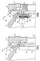
- FIG. 2 is a longitudinal half-section of one embodiment of an electron energy analyzer of the invention.
- FIG. 3 is a longitudinal half-section of another embodiment of an electron energy analyzer of the invention.
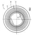
- FIG. 4 is a face view of an anode plate used in the invention of FIG. 3.
- FIG. 5 shows computer-generated electrical field lines associated with the embodiment of FIG. 3.
- FIG. 6 shows computer-generated electron trajectories associated with the embodiment of FIG. 3.
- FIG. 1 An electron energy analyzing system 10 ⁇ incorporating the invention is shown in FIG. 1.
- the components except those associated with a detector subassembly are conventional such as in a Model 25-120 ⁇ A Auger electron spectroscopy analyzer sold by The Perkin-Elmer Corporation.
- This figure is schematic; details may be found in references such as the aforementioned U.S. Patent No. 4,20 ⁇ 5,226.
- the analyzing system 10 ⁇ is enclosed in a multi-component housing 14 which is maintained at vacuum by an ion pump, these conventional components being not shown. For clarity other standard parts such as viewing ports, internal valving, sample mount and the like are also not shown.
- An electron gun 18 located on the axis 16 of the system may be any desired type such as may be based on electrostatic or magnetic optics, or thermionic or field emission of electrons.
- a target 20 ⁇ of sample material to be surface analyzed is placed at an outer end 22 of the system.
- the system is generally cylindrical, and all of the components located between the electron gun and the target have an axial passage 24 extending therethrough so that a primary electron or other energy beam 25 can be directed from the gun 18 onto the target.
- Electron optical components for the beam, shown generally at 26 may also be disposed coaxially as required, such as a variable aperture objective, steering plates, an objective lens, a deflector and a stigmator, some of which may be magnetic.
- the beam from the gun causes charged particles 27 to be emitted from the target.
- the particles may be positive ions, negative ions or electrons, for example Auger electrons.
- the axial beam 25 to the target may be an ion stream, X-rays or any other suitable energy source, and the emission may include reflected electrons.
- the present system has two energy analyzers operating in tandem with respect to emitted electrons 27 .
- the first, or primary analyzer is a conventional cylindrical mirror analyzer 30 ⁇ (CMA). This comprises an outer conductive cylinder 32 and an inner conductive cylinder 34 .
- the outer cylinder has a negative voltage relative to a reference voltage on the inner cylinder, the reference generally being ground potential. Voltages are provided by a DC source 36 via leads 38 in a through-fitting 40 ⁇ in the housing 14 .
- Electrons 27 diverging from the target within a certain range of conical angles pass through a first annular gap 42 and a grounded screen 43 and enter the space 44 between the cylinders. Because of the field associated with the negative voltage on the outer cylinder 32 , the electrons will follow a path 28 that curves back toward the axis 16 of the system. The exact path or trajectory for each electron is dependent on the kinetic energy of the electron relative to the field. Those electrons with an energy within a small range of energies will exit the space 44 through another grounded screen 45 and an annular passage 47 in the inner cylinder 34 , to be detected by a detection system 50 ⁇ located within the inner cylinder 34 opposite the target source 20 ⁇ .
- the conventional detection system is replaced by a specific type of second energy analyzer 50 ⁇ , for further measuring the spectrum within the energy range of electrons passing through the passage 47 .
- a simple embodiment of this secondary analyzer 50 ⁇ is shown schematically in FIG. 2. The components are symmetrical about an axis 16 which coincides with the axis of the system (FIG. 1).
- a body 52 which may be a portion of the inner cylinder 34 (although not so in the present example), has an annular opening 46 therein.
- the opening 46 is bounded by an outer wall 54 and an inner wall 56 of the body 52 , so that the opening generally faces outwardly and rearwardly toward input electrons passing from the cylindrical analyzer space 44 .
- each electron has a trajectory 28 with a radially inward directional component 43 and an axial directional component 45 in a forward direction (toward the right in the figures).
- a deflector means formed of a deflector electrode 68 with a surface 70 ⁇ is disposed coaxially in the body 52 generally with the surface perpendicular to the axis 16 so as to face toward the detector 58 .
- this electrode may have its surface 70 ⁇ extending inwardly to approximately the same inner radius as for the detector.
- the surface may be flat or conical within the purview of the invention.
- the voltage is positive; thus the voltage is positive or negative corresponding respectively to the charged particles being positive or negative.
- the axial directional component is reversed to an axial directional component 73 opposite the forward direction.
- the radial component 43′ may also be affected, possibly even reversed.
- this voltage has a magnitude corresponding approximately to an average of the electron energies (in election volts) of the input electrons 28 .
- a channel plate detector assembly 58 is disposed inwardly of the inner wall 56 and has an electron entry surface 60 ⁇ for the reversed-direction electrons and extends to a radius proximate the inner wall.
- the detector is washer-shaped with the entry surface 60 ⁇ coinciding with an entry area 62 that is perpendicular to the axis 16 , advantageously radially inward of the annular opening.
- An axial hole 66 in the detector 58 accommodates the central beam as explained above.
- the detector signals are sent via leads 69 to a data processor 71 (FIG. 1) for conversion to spectrographic information of energy distribution.
- This detector is sensitive to the radial position of the reversed electrons. Since such radial position is energy dependent, the position-sensitive detector measures energy distribution of the electrons.
- FIG. 3 (also shown in FIG. 1), the general configuration is similar except that the deflector means comprises two electrodes.
- a primary electrode 74 has a primary electrode surface 76 with an axi-symmetric concave curvature, or toroidal section, facing back toward the entry surface 60 ⁇ of the detector means.
- the voltage means 36 Via line 73 the voltage means 36 (FIG. 1) provides a negative (positive for positive ions) primary voltage to this electrode to deflect the electrons back to the detector means 58 .
- the curvature of the toroidal section approximates the average curvature of trajectories for deflected electrons which are explained below.
- a ring-shaped secondary electrode 78 has a secondary electrode surface 80 ⁇ disposed coaxially within the primary electrode surface so as to face toward the entry surface 60 ⁇ .
- the shape of the electrode surface 80 ⁇ is not critical and conveniently is a frusto-conical surface facing radially outward. This surface has a radial disposition within that of the entry surface, i.e. at about the same radius although axially spaced therefrom.
- the secondary electrode 78 has a negative (or positive in the case of positive ions) secondary voltage relative to the body and the detector means, the secondary voltage being less in magnitude than the primary voltage, and preferably about half of the primary voltage. This secondary voltage is derived [from the source 36 via a line 79 (FIG. 1).]
- the detector 58 is shown in some more detail in this figure with further details of the channel plate detector assembly being essentially as described in the aforementioned article by Wiza.
- a channel plate available from Galileo Electro-Optics Corp., Sturbridge Massachusetts, as "MCP-28”, has channels with 32 micron center-center spacing, each channel being 25 microns ID and one mm thick.
- the plate is given an annular (ring) shape.
- the detector comprises at least a single channel plate, and preferably a chevron pair of channel plates 82,84 at opposed 8 degrees each as disclosed in Wiza to block ion back drift.
- the entry surface 60 ⁇ is planar, as is typical of a channel plate surface.
- An anode plate 86 of an insulating base 87 with a plurality of annular anode rings (collectively designated 88 in FIG. 4) is placed behind the channel plates to receive the multiplied electron flow.
- the voltages between plates is, e.g., +10 ⁇ 0 ⁇ 0 ⁇ V
- voltage on the backside 90 ⁇ is +20 ⁇ 0 ⁇ 0 ⁇ V
- the voltage on the anode plate rings is +220 ⁇ 0 ⁇ V.
- FIG. 3 illustrates a system for digital detection using a set of arcuately spaced capacitors (one shown at 92 ) of 20 ⁇ 0 ⁇ picofarads each leading from a different anode ring through connection leads 69 (FIG. 1) to an electronic amplifier-processor 71 with display or other presentation of data.
- FIG. 5 shows computer-generated equipotential field lines 94 associated with the illustrated configuration, a primary electrode voltage of -1535 volts, and a secondary electrode voltage of -767.5 volts.
- the lines may be seen to be denser in the region 96 between the detector surface 60 ⁇ and the primary electrode 74 than in the region 98 between the detector surface and the secondary electrode 78 . This effect is believed to contribute to the beneficial results achieved with this configuration, described below.
- the spacial separation of the outer edge 10 ⁇ 1 of the entry surface 60 ⁇ should be relatively small. More specifically this separation should be substantially less than the spacial separation of the entry surface from the primary electrode surface 76 , preferably less than about one quarter of the latter separation. As previously indicated, the body including wall 56 and the surface 60 ⁇ should both be at ground potential.
- FIG. 6 shows computer-generated electron trajectories 10 ⁇ 0 ⁇ through the field shown in FIG. 5.
- the trajectories were initiated at the center of the target surface with polar angles at the target from 35.2 to 47.2 degrees and with four energies from 1520 ⁇ eV to 1548 eV in 9 1/3 eV increments. These trajectories are shown in fully darkened patterns of four bundles, 10 ⁇ 2,10 ⁇ 4,10 ⁇ 6,10 ⁇ 8, one for each energy, with zero energy band width.
- the trajectories were traced through a cylindrical analyzer with a 16.25 cm diameter outer cylinder, 7.5 cm diameter inner cylinder, and -10 ⁇ 0 ⁇ 0 ⁇ V applied to the outer cylinder.
- the target surface 20 ⁇ was 18.7 cm from the detector surface 60 ⁇ (FIG.
- the scale of the secondary analyzer is shown in the FIG. 6.
- the inner cylinder, the second analyzer body and the input surface of the channel detector were electrically grounded.
- the primary and secondary deflection electrodes 74,78 had applied potentials of -1535 V and -767.5 V respectively, for the computer-generated paths.
- Focus, or crossover, of the electrons from the CMA is substantially at the annular opening and in a conical surface at the conventional 23 degree angle to the axis.
- Particles with the highest kinetic energy trajectories 10 ⁇ 2 penetrate the farthest into the deflecting field and lose the most energy because of the deep penetration. These are deflected the most and strike the channel plate near its outer radius.
- the lowest energy particles 10 ⁇ 8 penetrate the least and lose the least amount of energy, and travel to the channel plate nearest the axis.
- the energy dispersion across the channel plate detector 58 is generally nonlinear. This is readily compensated by selected radial positions of the annular rings 88 on the anode plate, as shown in FIG. 4 for eight rings.
- the rings are connected electrically through to a conductive pattern (not shown) on the backside of the plate with appropriate resistors to the DC source to bias the anodes.
- the capacitors 92 couple the signals to amplifiers (incorporated in processor 71 , FIG. 1) at near ground potential.
- Central hole 112 is for mounting and the axial channel 24 (FIG. 1). Conductive area 114 is raised to contact the second channel plate backside 90 ⁇ for application of the appropriate voltage.
- the distribution of electron energies may be defined as a set of energy bands each having an energy band width, and the radial distances of the electrons at the plane may be organized as a set of annular channels each corresponding to an energy band and having a correspondingly selected radial width.
- Each annular ring 88 of the anode plate then has a different ring width W (shown only for outer ring 116 ) corresponding to a selected radial width of a corresponding annular channel and thereby to a corresponding energy band. This results in detection channels that have approximately equal energy resolution.
- the expected performance of such a multichannel analyzer can be estimated from and compared with that of a single channel CMA operated at 0 ⁇ .3% energy resolution and with the same angular acceptance.
- the single channel CMA count rate under standard Auger measurement conditions is about 10 ⁇ 0 ⁇ kcps (thousand counts per second) above background.
- the present invention should be suitable with other axi-symmetrical configurations for the primary electron energy analyzer.
- An example is an analyzer with inner and outer curved conductors in place of the cylindrical conductors.
- the system need not have the full 360 ⁇ degree azimuthal or cylindrical configuration and, for example may be hemicylindrical.
- axi-symmetrical, annular and the like as related to the axi-symmetry of the system and its analyzer, deflection and detector components, are intended to include such partially cylindrical configurations, since it will be appreciated that the principles of operation are the same.
Landscapes
- Chemical & Material Sciences (AREA)
- Analytical Chemistry (AREA)
- Electron Tubes For Measurement (AREA)
- Analysing Materials By The Use Of Radiation (AREA)
Description
- This invention relates to charged-particle energy analyzing systems generally used for characterizing sample surfaces, and particularly to such a system incorporating an additional multichannel charged particle analyzer.
- Instrumentation for use in spectroscopy of charged particles makes use of electrons or ions which are emitted from a substance after being bombarded or irradiated with electrons or ions from a source such as an electron gun. A technique to which the invention is particularly directed is known as Auger electron spectroscopy. In this technique, a target sample material is placed in a vacuum, usually below 1,33·10̸⁻⁵ Pa (10̸⁻⁷ Torr), and upon being bombarded with electrons from some source, such as an electron gun, the sample gives off a variety of emissions. Among these are X-rays, secondary electrons, and reflected primary electrons from the source. The emissions include Auger electrons (a particular class of secondary electrons) in the manner which is well known in the literature.
- In the art of Auger electron spectroscopy, as taught for example in U.S. Patent No. 4,20̸5,226 (Gerlach), of the present assignee, instruments making use of cylindrical mirror analyzers ("CMA") are known which analyze the energy and the energy spectrum of Auger electrons emitted by the sample material. Such instruments operate by injecting the diverging electrons into a radial electric field produced between a pair of coaxially mounted electrode cylinders held at different electric potentials. Auger electrons injected from the sample into the radial electric field between the cylindrical electrodes are deflected by the field back toward the common axis of the electrodes. Electrons of a predetermined energy are thereby brought to a focus. By positioning a collector apparatus at this focus, electrons of a predetermined energy are selected and detected. By sweeping the voltage impressed across the cylindrical electrodes through a range of values, and detecting as a function of these applied potentials such electrons as are collected, the energy spectrum of the injected electrons may be plotted and determined.
- As disclosed in the aforementioned patent, it is advantageous to utilize a detector system that is off-axis, for example annular, because the central axis is used for the primary beam to the target. Also, magnetic lenses used for the electron gun deflect paths of electrons being detected, thus interfering with precision measurements. German Patent Application No. 27 0̸5 430̸ similarly discloses off-axis detection in several configurations and electron paths, representing efforts to increase sensitivity. U.S. Patent No. 4,10̸0̸,40̸9 teaches bringing the electron gun beam from off-axis, eliminating magnetic lenses, and then utilizing an on-axis detector system to receive electrons from the cylindrical analyzer.
- In an article "A Cylindrical Mirror Photoelectron Spectrometer With Position-Sensitive Detector Used For X-Ray Analysis" by O. Benka, Nuclear Instruments and Methods, 20̸3, 547-550̸ (1982) there is described a CMA with a position sensitive detector positioned off-axis for multichannel detection of electrons leaving the CMA, to increase instrument sensitivity. The high precision detector useful for such an application is a channel plate detector of the type disclosed in an article "Microchannel Plate Detectors" by J. L. Wiza, Nuclear Instruments and Methods, 162, 587-60̸1 (1979). Such a detector includes a ceramic plate formed with a large number of microchannels therethrough, each microchannel being an electron multiplier of incident electrons or ions.
- The channel plate detector is quite effective but, because of its inherent construction, has generally been available commercially as a flat ceramic plate with a planar electron entry surface. Recently curved plate technology has become available on a limited basis but is extremely expensive. Therefore, Benka placed such a channel detector plate in only a small (40̸ degree) azimuthal portion of the 360̸ degree CMA. He further utilized a 6 degree polar range (12 degrees is actually more standard), and reported measuring 6.5% of the electron energy spectrum with 0̸.3% resolution. This result was actually an 18 times decrease in angular acceptance. This could be improved upon by utilizing a ring of such plates, but such an assembly would be a cumbersome and costly solution and still may not provide optimum sensitivity.
- An object of the present invention is to provide a novel charged-particle energy analyzer useful for improving sensitivity of an axi-symmetrical energy analyzing system. Another object is to provide such an analyzer having an axial opening therethrough available for an axially-directed primary energy beam in the system. Further objects are to provide for sensitive off-axis detection of electrons, and to improve signal-to-noise ratio. Yet another object is to provide an improved energy analyzer incorporating a channel plate detector so as to detect substantially a full 360̸° azimuthal range of particles having a distribution of energies.
- The foregoing and other objectives are achieved with a charged particle energy analyzer comprising a hollow axi-symmetrical body with an annular opening therein coaxial to a central axis. The annular opening is receptive of input charged particles from an energy dispersing means such as a cylindrical mirror analyzer.
- The input particles have a distribution of particle energies and a range of particle trajectories, the trajectories each having a radially inward directional component and an axial directional component in a forward direction parallel to the axis. A deflection means is disposed coaxially in the body so as to be receptive of the input particles for reversing the axial directional component of each of the trajectories, and directing the particles oppositely from the forward direction through an axi-symmetrical entry area such that radial distances of the electrons from the axis at the entry area are associated with the electron energies. A detector means is disposed in the body with an entry surface coinciding with the entry area for detecting the electrons at the entry area relative to radial distance. Such a configuration allows the analyzer to have an axial passage therethrough for a central energy beam directed to a target source of the charged particles.
- In a preferred embodiment the deflection means comprises a pair of electrodes. A primary electrode with an annular primary electrode surface is disposed coaxially in the body generally perpendicular to the axis so as to face toward the entry surface, The primary electrode surface has an axi-symmetric concave curvature facing toward the entry surface. A secondary electrode with a secondary electrode surface is disposed coaxially within and in general axial alignment with the primary electrode surface so as to face toward the entry surface. A primary voltage is effected on the primary electrode relative to the detector means being at ground potential, and a secondary voltage is effected on the secondary electrode relative to the detector means. The voltages are positive or negative corresponding respectively to the charged particles being positive or negative. The secondary voltage is less in magnitude than the primary voltage.
- Advantageously the detector means is an annular channel plate detector assembly. A channel plate with a matrix of electron multiplier channels is receptive of the charged particles at the planar entry area and passing through to a backside of the channel plate. An anode plate communicates with the channels at the backside and is formed with a plurality of annular anode rings coaxial to the axis so that each anode ring receives electrons from the channel plate according to radial distance of the electrons from the axis.
- FIG. 1 is a simplified longitudinal section of a cylindrical mirror analyzer system incorporating an electron energy analyzer according to the invention.
- FIG. 2 is a longitudinal half-section of one embodiment of an electron energy analyzer of the invention.
- FIG. 3 is a longitudinal half-section of another embodiment of an electron energy analyzer of the invention.
- FIG. 4 is a face view of an anode plate used in the invention of FIG. 3.
- FIG. 5 shows computer-generated electrical field lines associated with the embodiment of FIG. 3.
- FIG. 6 shows computer-generated electron trajectories associated with the embodiment of FIG. 3.
- An electron energy analyzing system 10̸ incorporating the invention is shown in FIG. 1. Generally the components except those associated with a detector subassembly are conventional such as in a Model 25-120̸A Auger electron spectroscopy analyzer sold by The Perkin-Elmer Corporation. This figure is schematic; details may be found in references such as the aforementioned U.S. Patent No. 4,20̸5,226.
- The analyzing system 10̸ is enclosed in a
multi-component housing 14 which is maintained at vacuum by an ion pump, these conventional components being not shown. For clarity other standard parts such as viewing ports, internal valving, sample mount and the like are also not shown. Anelectron gun 18 located on theaxis 16 of the system may be any desired type such as may be based on electrostatic or magnetic optics, or thermionic or field emission of electrons. A target 20̸ of sample material to be surface analyzed is placed at anouter end 22 of the system. The system is generally cylindrical, and all of the components located between the electron gun and the target have anaxial passage 24 extending therethrough so that a primary electron orother energy beam 25 can be directed from thegun 18 onto the target. Electron optical components for the beam, shown generally at 26 may also be disposed coaxially as required, such as a variable aperture objective, steering plates, an objective lens, a deflector and a stigmator, some of which may be magnetic. - The beam from the gun causes charged
particles 27 to be emitted from the target. The particles may be positive ions, negative ions or electrons, for example Auger electrons. In other cases theaxial beam 25 to the target may be an ion stream, X-rays or any other suitable energy source, and the emission may include reflected electrons. - The present system has two energy analyzers operating in tandem with respect to emitted
electrons 27. The first, or primary analyzer is a conventional cylindrical mirror analyzer 30̸ (CMA). This comprises an outerconductive cylinder 32 and an innerconductive cylinder 34. The outer cylinder has a negative voltage relative to a reference voltage on the inner cylinder, the reference generally being ground potential. Voltages are provided by aDC source 36 vialeads 38 in a through-fitting 40̸ in thehousing 14. -
Electrons 27 diverging from the target within a certain range of conical angles pass through a firstannular gap 42 and a groundedscreen 43 and enter thespace 44 between the cylinders. Because of the field associated with the negative voltage on theouter cylinder 32, the electrons will follow apath 28 that curves back toward theaxis 16 of the system. The exact path or trajectory for each electron is dependent on the kinetic energy of the electron relative to the field. Those electrons with an energy within a small range of energies will exit thespace 44 through another groundedscreen 45 and anannular passage 47 in theinner cylinder 34, to be detected by a detection system 50̸ located within theinner cylinder 34 opposite the target source 20̸. - In the prior analyzer, disclosed in the aforementioned U.S. Patent No. 4,20̸5,226, a small annular opening is provided for the electron detector. By changing the voltage on the outer cylinder the energy band selected by the detector is changed correspondingly. Thus scanning of the voltage combined with electron detection of electrons transmitting the gap provides a spectrum which may be correlated with characteristics of the target, such as material and topography.
- According to the present invention the conventional detection system is replaced by a specific type of second energy analyzer 50̸, for further measuring the spectrum within the energy range of electrons passing through the
passage 47. A simple embodiment of this secondary analyzer 50̸ is shown schematically in FIG. 2. The components are symmetrical about anaxis 16 which coincides with the axis of the system (FIG. 1). Abody 52, which may be a portion of the inner cylinder 34 (although not so in the present example), has anannular opening 46 therein. - The
opening 46 is bounded by anouter wall 54 and aninner wall 56 of thebody 52, so that the opening generally faces outwardly and rearwardly toward input electrons passing from thecylindrical analyzer space 44. At theannular opening 46 each electron has atrajectory 28 with a radially inwarddirectional component 43 and an axialdirectional component 45 in a forward direction (toward the right in the figures). - A deflector means formed of a
deflector electrode 68 with a surface 70̸ is disposed coaxially in thebody 52 generally with the surface perpendicular to theaxis 16 so as to face toward thedetector 58. In this simple embodiment this electrode may have its surface 70̸ extending inwardly to approximately the same inner radius as for the detector. Although preferably axi-symmetrically curved as shown, the surface may be flat or conical within the purview of the invention. A negative voltage vialine 73 from source 36 (FIG. 1) on this electrode, relative to thebody 52 and detector entry surface 60̸ being at the reference (ground) voltage, deflects the incoming electrons back toward adetector 58 as shown at path location 72. In the case of the charged particles being positive ions, the voltage is positive; thus the voltage is positive or negative corresponding respectively to the charged particles being positive or negative. In either case the axial directional component is reversed to an axialdirectional component 73 opposite the forward direction. Theradial component 43′ may also be affected, possibly even reversed. Preferably this voltage has a magnitude corresponding approximately to an average of the electron energies (in election volts) of theinput electrons 28. - A channel
plate detector assembly 58 is disposed inwardly of theinner wall 56 and has an electron entry surface 60̸ for the reversed-direction electrons and extends to a radius proximate the inner wall. The detector is washer-shaped with the entry surface 60̸ coinciding with anentry area 62 that is perpendicular to theaxis 16, advantageously radially inward of the annular opening. Anaxial hole 66 in thedetector 58 accommodates the central beam as explained above. The detector signals are sent vialeads 69 to a data processor 71 (FIG. 1) for conversion to spectrographic information of energy distribution. This detector is sensitive to the radial position of the reversed electrons. Since such radial position is energy dependent, the position-sensitive detector measures energy distribution of the electrons. - In a preferred embodiment, FIG. 3 (also shown in FIG. 1), the general configuration is similar except that the deflector means comprises two electrodes. A
primary electrode 74 has aprimary electrode surface 76 with an axi-symmetric concave curvature, or toroidal section, facing back toward the entry surface 60̸ of the detector means. Vialine 73 the voltage means 36 (FIG. 1) provides a negative (positive for positive ions) primary voltage to this electrode to deflect the electrons back to the detector means 58. The curvature of the toroidal section approximates the average curvature of trajectories for deflected electrons which are explained below. - A ring-shaped
secondary electrode 78 has a secondary electrode surface 80̸ disposed coaxially within the primary electrode surface so as to face toward the entry surface 60̸. The shape of the electrode surface 80̸ is not critical and conveniently is a frusto-conical surface facing radially outward. This surface has a radial disposition within that of the entry surface, i.e. at about the same radius although axially spaced therefrom. Thesecondary electrode 78 has a negative (or positive in the case of positive ions) secondary voltage relative to the body and the detector means, the secondary voltage being less in magnitude than the primary voltage, and preferably about half of the primary voltage. This secondary voltage is derived [from thesource 36 via a line 79 (FIG. 1).] - The
detector 58 is shown in some more detail in this figure with further details of the channel plate detector assembly being essentially as described in the aforementioned article by Wiza. A channel plate available from Galileo Electro-Optics Corp., Sturbridge Massachusetts, as "MCP-28", has channels with 32 micron center-center spacing, each channel being 25 microns ID and one mm thick. The plate is given an annular (ring) shape. The detector comprises at least a single channel plate, and preferably a chevron pair ofchannel plates - An
anode plate 86 of an insulatingbase 87 with a plurality of annular anode rings (collectively designated 88 in FIG. 4) is placed behind the channel plates to receive the multiplied electron flow. With the electron entry surface 60̸ at reference (ground) potential, the voltages between plates is, e.g., +10̸0̸0̸ V, voltage on the backside 90̸ is +20̸0̸0̸ V, and the voltage on the anode plate rings is +220̸0̸ V. Measurement of electrons cascaded from the input electrons or ions is made conventionally either by current flow with analog detection or by electron counts with digital detection. FIG. 3 illustrates a system for digital detection using a set of arcuately spaced capacitors (one shown at 92) of 20̸0̸ picofarads each leading from a different anode ring through connection leads 69 (FIG. 1) to an electronic amplifier-processor 71 with display or other presentation of data. - FIG. 5 shows computer-generated
equipotential field lines 94 associated with the illustrated configuration, a primary electrode voltage of -1535 volts, and a secondary electrode voltage of -767.5 volts. The lines may be seen to be denser in theregion 96 between the detector surface 60̸ and theprimary electrode 74 than in theregion 98 between the detector surface and thesecondary electrode 78. This effect is believed to contribute to the beneficial results achieved with this configuration, described below. - In order to minimize influence of any electrical field in the
gap 99 between theinner wall 56 and thedetector 58, the spacial separation of the outer edge 10̸1 of the entry surface 60̸ should be relatively small. More specifically this separation should be substantially less than the spacial separation of the entry surface from theprimary electrode surface 76, preferably less than about one quarter of the latter separation. As previously indicated, thebody including wall 56 and the surface 60̸ should both be at ground potential. - FIG. 6 shows computer-generated electron trajectories 10̸0̸ through the field shown in FIG. 5. The trajectories were initiated at the center of the target surface with polar angles at the target from 35.2 to 47.2 degrees and with four energies from 1520̸ eV to 1548 eV in 9 1/3 eV increments. These trajectories are shown in fully darkened patterns of four bundles, 10̸2,10̸4,10̸6,10̸8, one for each energy, with zero energy band width. The trajectories were traced through a cylindrical analyzer with a 16.25 cm diameter outer cylinder, 7.5 cm diameter inner cylinder, and -10̸0̸0̸ V applied to the outer cylinder. The target surface 20̸ was 18.7 cm from the detector surface 60̸ (FIG. 1). The scale of the secondary analyzer is shown in the FIG. 6. The inner cylinder, the second analyzer body and the input surface of the channel detector were electrically grounded. The primary and
secondary deflection electrodes - Focus, or crossover, of the electrons from the CMA is substantially at the annular opening and in a conical surface at the conventional 23 degree angle to the axis. Particles with the highest kinetic energy trajectories 10̸2 penetrate the farthest into the deflecting field and lose the most energy because of the deep penetration. These are deflected the most and strike the channel plate near its outer radius. Conversely, the lowest energy particles 10̸8 penetrate the least and lose the least amount of energy, and travel to the channel plate nearest the axis. There is also a focusing effect of the medium and lower energy electrons 10̸4,10̸6,10̸8.
- The energy dispersion across the
channel plate detector 58 is generally nonlinear. This is readily compensated by selected radial positions of the annular rings 88 on the anode plate, as shown in FIG. 4 for eight rings. The rings are connected electrically through to a conductive pattern (not shown) on the backside of the plate with appropriate resistors to the DC source to bias the anodes. For pulse counting thecapacitors 92 couple the signals to amplifiers (incorporated inprocessor 71, FIG. 1) at near ground potential.Central hole 112 is for mounting and the axial channel 24 (FIG. 1).Conductive area 114 is raised to contact the second channel plate backside 90̸ for application of the appropriate voltage. - The distribution of electron energies may be defined as a set of energy bands each having an energy band width, and the radial distances of the electrons at the plane may be organized as a set of annular channels each corresponding to an energy band and having a correspondingly selected radial width. Each
annular ring 88 of the anode plate then has a different ring width W (shown only for outer ring 116) corresponding to a selected radial width of a corresponding annular channel and thereby to a corresponding energy band. This results in detection channels that have approximately equal energy resolution. - The expected performance of such a multichannel analyzer can be estimated from and compared with that of a single channel CMA operated at 0̸.3% energy resolution and with the same angular acceptance. The single channel CMA count rate under standard Auger measurement conditions is about 10̸0̸ kcps (thousand counts per second) above background. Given 8 energy channels in the present multichannel CMA system with a secondary analyzer, and a 60̸% channel plate efficiency (compared to single channel detection), the multichannel CMA count rate will be about 8*10̸0̸*60̸% = 50̸0̸ kpcs above background with the same 0̸.3% energy resolution.
- Also, there is significant background noise in a conventional CMA due to scattering in the analyzer to the annular opening at the focal plane. The secondary analyzer effectively screens out a large portion of the scattered electrons outside of the energy range established for the analyzer. This results in a significant increase in signal-to-background ratio.
- Although described herein for a CMA, the present invention should be suitable with other axi-symmetrical configurations for the primary electron energy analyzer. An example is an analyzer with inner and outer curved conductors in place of the cylindrical conductors. Also, the system need not have the full 360̸ degree azimuthal or cylindrical configuration and, for example may be hemicylindrical. As used herein and in the claims, the terms axi-symmetrical, annular and the like as related to the axi-symmetry of the system and its analyzer, deflection and detector components, are intended to include such partially cylindrical configurations, since it will be appreciated that the principles of operation are the same.
- While the invention has been described above in detail with reference to specific embodiments, various changes and modifications which fall within the scope of the appended claims will become apparent to those skilled in this art. Therefore, the invention is intended only to be limited by the scope of the appended claims.
Claims (25)
- A charged particle energy analyzer (50̸) comprising:
a hollow axi-symmetrical body (52) with an annular opening (46) therein coaxial to a central axis (16), the annular opening being receptive of input charged particles having a distribution of particle energies and a range of particle trajectories (28), the trajectories each having a radially inward directional component (43) and an axial directional component (45) in a forward direction parallel to the axis;
deflection means (68; 74, 78) disposed coaxially in the body so as to be receptive of the input charged particles for reversing axial directional components of the trajectories and directing the charged particles oppositely from the forward direction through an axi-symmetrical entry area (62) such that radial distances of the charged particles from the axis at the entry area are associated with the particle energies; and
detector means (58) with an entry surface (60̸) coinciding with the entry area for detecting the charged particles at the entry area relative to radial distance. - The analyser according to Claim 1 wherein the entry surface is disposed radially inward of the annular opening.
- The analyser according to Claim 1 wherein the deflection means comprises a primary electrode disposed coaxially in the body with a primary electrode surface generally perpendicular to the axis so as to face toward the entry surface, and further comprises voltage means for effecting a primary voltage on the primary electrode relative to the detector means, the primary voltage being positive or negative corresponding respectively to the charged particles being positive or negative.
- The analyzer according to Claim 3 wherein the primary voltage has a magnitude corresponding approximately to an average of the particle energies.
- The analyzer according to Claim 3 wherein the primary electrode surface has an axi-symmetric concave curvature facing toward the entry surface.
- The analyzer according to Claim 5 wherein the primary electrode is annular, the deflection means further comprises a secondary electrode with a secondary electrode surface disposed coaxially within and in general axial alignment with the primary electrode surface so as to face toward the entry surface, and the voltage means further effects a secondary voltage on the secondary electrode relative to the body and the detector means, the secondary voltage being less in magnitude than the primary voltage and being positive or negative corresponding respectively to the primary voltage being positive or negative.
- The analyzer according to Claim 6 wherein the secondary voltage is about half of the primary voltage.
- The analyzer according to Claim 6 wherein the secondary electrode surface is a frusto-conical surface facing radially outward toward the detector means.
- The analyzer according to Claim 3 wherein the annular opening is bounded on one side by an outer wall of the body and on the opposite side by an inner wall of the body disposed radially inward of the outer wall, the entry surface has an outer edge with a first spacial separation radially inward from the inner wall and a second spacial separation from the primary electrode surface, the first spacial separation is substantially less than the second spacial separation, and the voltage means effects a reference voltage in common to both the entry surface and the body.
- The analyzer according to Claim 9 wherein the first spacial separation is less than about one quarter of the second spacial separation.
- The analyzer according to Claim 1 wherein the entry surface is planar.
- The analyzer according to Claim 11 wherein the detector means is a channel plate detector assembly.
- The analyzer according to Claim 12 wherein the channel plate detector assembly comprises an annular channel plate with a matrix of electron multiplier channels receptive of the charged particles at the entry area and passing through to a backside of the channel plate, and further comprises an anode plate communicating with the channels at the backside, the anode plate being formed with a plurality of annular anode rings coaxial to the axis so that each anode ring receives electrons from the channel plate according to radial distance of the charged particles from the axis.
- The analyzer according to Claim 13 wherein the distribution of particle energies comprises a set of energy bands each having an energy band width, the radial distances of the electrons at the entry surface are organized as a set of annular channels each associated with an energy band and having a corresponding radial width, and each anode ring has a ring width associated with a radial width of a corresponding annular channel and is thereby associated with a corresponding energy band.
- The analyzer according to Claim 14 wherein the energy band widths are substantially equal.
- The analyzer according to Claim 1 wherein the analyzer has an axial passage therethrough.
- The analyzer according to Claim 1 further comprising particle energy dispersement means for effecting the input charged particles to the annular opening.
- The analyzer according to Claim 17 wherein the dispersement means focuses input charged particles substantially at the annular opening spacially according to particle energy.
- The analyzer according to Claim 18 wherein the dispersement means comprises a cylindrical mirror analyzer.
- The analyzer according to Claim 19 wherein the charged particle energy analyzer has an axial passage therethrough and further comprises target means for retaining a target source on the central axis for emitting charged particles into the dispersement means, and beam generating means for directing an energy beam through the axial passage to the target source so as to effect emitting of the charged particles from the target source.
- The analyzer according to Claim 1 wherein the charged particles are electrons.
- An electron energy analyzer (50̸) comprising:
a hollow axi-symmetrical body (52) with an annular opening (46) therein coaxial to a central axis (16), the annular opening being receptive of input electrons having a distribution of electron energies and a range of electron trajectories (28), the trajectories each having a radially inward directional component (43) and an axial directional component (45) in a forward direction parallel to the axis;
deflection means (68; 74, 78) disposed coaxially in the body so as to reverse the axial directional components of the electron trajectories and direct the electrons oppositely from the forward direction through an axi-symmetric planar entry area (62) such that radial distances of the electrons from the axis at the entry area are associated with the electron energies; and
a channel plate detector assembly (58) disposed in the body and having a planar entry surface (60̸) coinciding with the entry area for detecting the electrons at the entry area relative to radial distance, the channel plate detector having an axial passage therethrough;
the deflection means comprising a primary electrode (74) with an axial opening therethrough and having an axi-symmetric concave surface (76) disposed coaxially in the body generally perpendicular to the axis so as to face toward the entry surface, a secondary electrode (78) with a central passage therethrough and a frusto-conical surface (80̸) disposed coaxially within and in general axial alignment with the primary electrode surface so as to face radially outward toward the entry surface, and voltage means for effecting a negative primary voltage on the primary electrode and a negative secondary voltage on the secondary electrode, the primary and secondary voltages each being relative to the body and the entry surface, and the secondary voltage being less in magnitude than the primary voltage. - The analyzer according to Claim 22 wherein the annular opening is bounded on one side by an outer wall of the body and on the opposite side by an inner wall of the body disposed radially inward of the outer wall, the entry surface has an outer edge with a first spacial separation radially inward from the inner wall and a second spacial separation from the primary electrode surface, the first spacial separation is substantially less than the second spacial separation, and the voltage means effects a reference voltage in common to both the entry surface and the body.
- The analyzer according to Claim 22 wherein the channel plate detector assembly comprises a channel plate with a matrix of electron multiplier channels receptive of the electrons at the plane and passing through to a backside of the channel plate, and further comprises an anode plate communicating with the channels at the backside, the anode plate being formed with a plurality of annular anode rings coaxial to the axis so that each anode ring receives electrons from the channel plate according to radial distance of the electrons from the axis, and wherein the distribution of electron energies comprises a set of energy bands each having an energy band width, the radial distances of the electrons at the entry surface are organized as a set of annular channels each associated with an energy band and having a corresponding radial width, and each anode ring has a ring width associated with radial width of a corresponding annular channel and is thereby associated with a corresponding energy band.
- The analyzers according to Claim 22 wherein the analyzer has a central passage therethrough and further comprises beam generating means for directing an energy beam through the axial passage to a target source so as to effect electron emission therefrom, and a cylindrical mirror analyzer receptive of the electron emission for effecting the input electrons and focusing the same at the annular opening spacially according to electron energy.
Applications Claiming Priority (2)
| Application Number | Priority Date | Filing Date | Title |
|---|---|---|---|
| US565289 | 1990-08-09 | ||
| US07/565,289 US5032724A (en) | 1990-08-09 | 1990-08-09 | Multichannel charged-particle analyzer |
Publications (3)
| Publication Number | Publication Date |
|---|---|
| EP0470478A2 EP0470478A2 (en) | 1992-02-12 |
| EP0470478A3 EP0470478A3 (en) | 1993-05-12 |
| EP0470478B1 true EP0470478B1 (en) | 1995-12-20 |
Family
ID=24257954
Family Applications (1)
| Application Number | Title | Priority Date | Filing Date |
|---|---|---|---|
| EP91112735A Expired - Lifetime EP0470478B1 (en) | 1990-08-09 | 1991-07-29 | Multichannel charged-particle analyzer |
Country Status (4)
| Country | Link |
|---|---|
| US (1) | US5032724A (en) |
| EP (1) | EP0470478B1 (en) |
| JP (1) | JP3140094B2 (en) |
| DE (1) | DE69115589T2 (en) |
Families Citing this family (14)
| Publication number | Priority date | Publication date | Assignee | Title |
|---|---|---|---|---|
| GB9220097D0 (en) * | 1992-09-23 | 1992-11-04 | Univ York | Electron spectrometers |
| US5900667A (en) * | 1996-10-04 | 1999-05-04 | Etec Systems, Inc. | Operating a solid state particle detector within a magnetic deflection field so as to minimize eddy currents |
| US6184523B1 (en) * | 1998-07-14 | 2001-02-06 | Board Of Regents Of The University Of Nebraska | High resolution charged particle-energy detecting, multiple sequential stage, compact, small diameter, retractable cylindrical mirror analyzer system, and method of use |
| JP4763191B2 (en) | 1999-06-16 | 2011-08-31 | シマヅ リサーチ ラボラトリー(ヨーロッパ)リミティド | Charged particle energy analyzer |
| EP1063677B1 (en) * | 1999-06-23 | 2005-03-16 | ICT Integrated Circuit Testing Gesellschaft für Halbleiterprüftechnik mbH | Charged particle beam device |
| GB0225791D0 (en) * | 2002-11-05 | 2002-12-11 | Kratos Analytical Ltd | Charged particle spectrometer and detector therefor |
| US7561438B1 (en) | 2004-12-22 | 2009-07-14 | Revera Incorporated | Electronic device incorporating a multilayered capacitor formed on a printed circuit board |
| JP4576272B2 (en) * | 2005-03-31 | 2010-11-04 | 株式会社日立ハイテクノロジーズ | electronic microscope |
| WO2007053843A2 (en) * | 2005-11-01 | 2007-05-10 | The Regents Of The University Of Colorado | Multichannel energy analyzer for charged particles |
| EP2245648A4 (en) * | 2008-01-25 | 2017-03-29 | Ionwerks, Inc. | Time-of-flight mass spectrometry of surfaces |
| US8071942B2 (en) * | 2009-03-20 | 2011-12-06 | Physical Electronics USA, Inc. | Sample holder apparatus to reduce energy of electrons in an analyzer system and method |
| KR101711145B1 (en) * | 2010-09-03 | 2017-03-13 | 삼성전자주식회사 | Portable quadrupole ion trap mass spectrometer |
| WO2012148358A1 (en) * | 2011-04-28 | 2012-11-01 | National University Of Singapore | A parallel radial mirror analyser for scanning microscopes |
| DE102013006535B4 (en) * | 2013-04-15 | 2025-11-06 | Carl Zeiss Microscopy Gmbh | Scanning particle beam microscope with energy-filtering detector system |
Family Cites Families (8)
| Publication number | Priority date | Publication date | Assignee | Title |
|---|---|---|---|---|
| US3609352A (en) * | 1970-05-18 | 1971-09-28 | Gen Electric | Secondary electron energy analyzing apparatus |
| US3805057A (en) * | 1971-03-22 | 1974-04-16 | Hitachi Ltd | Energy analyzer of coaxial cylindrical type |
| US3699331A (en) * | 1971-08-27 | 1972-10-17 | Paul W Palmberg | Double pass coaxial cylinder analyzer with retarding spherical grids |
| US3742214A (en) * | 1971-10-18 | 1973-06-26 | Varian Associates | Apparatus for performing chemical analysis by electron spectroscopy |
| US4100409A (en) * | 1973-02-02 | 1978-07-11 | U.S. Phillips Corporation | Device for analyzing a surface layer by means of ion scattering |
| NL7306378A (en) * | 1973-05-08 | 1974-11-12 | ||
| US4107526A (en) * | 1976-03-22 | 1978-08-15 | Minnesota Mining And Manufacturing Company | Ion scattering spectrometer with modified bias |
| US4205226A (en) * | 1978-09-01 | 1980-05-27 | The Perkin-Elmer Corporation | Auger electron spectroscopy |
-
1990
- 1990-08-09 US US07/565,289 patent/US5032724A/en not_active Expired - Lifetime
-
1991
- 1991-07-25 JP JP03186501A patent/JP3140094B2/en not_active Expired - Fee Related
- 1991-07-29 DE DE69115589T patent/DE69115589T2/en not_active Expired - Fee Related
- 1991-07-29 EP EP91112735A patent/EP0470478B1/en not_active Expired - Lifetime
Also Published As
| Publication number | Publication date |
|---|---|
| EP0470478A3 (en) | 1993-05-12 |
| EP0470478A2 (en) | 1992-02-12 |
| DE69115589T2 (en) | 1996-05-02 |
| JPH04233152A (en) | 1992-08-21 |
| US5032724A (en) | 1991-07-16 |
| DE69115589D1 (en) | 1996-02-01 |
| JP3140094B2 (en) | 2001-03-05 |
Similar Documents
| Publication | Publication Date | Title |
|---|---|---|
| EP0246841B1 (en) | Electron spectrometer | |
| CA1269181A (en) | Mass spectrometer for positive and negative ions | |
| US5032724A (en) | Multichannel charged-particle analyzer | |
| CN112305002B (en) | Spectroscopy and imaging system | |
| US6984821B1 (en) | Mass spectrometer and methods of increasing dispersion between ion beams | |
| EP0345605A1 (en) | Mass spectrometer | |
| US5091645A (en) | Selectable-resolution charged-particle beam analyzers | |
| US5834770A (en) | Ion collecting electrode for total pressure collector | |
| US4126782A (en) | Electrostatic charged-particle analyzer | |
| US8866103B2 (en) | Charged particle energy analysers and methods of operating charged particle energy analysers | |
| EP3417474A1 (en) | Extraction system for charged secondary particles for use in a mass spectrometer or other charged particle device | |
| JPH03173054A (en) | Particle radiation device | |
| US5134287A (en) | Double-focussing mass spectrometer | |
| WO1989006436A1 (en) | Secondary ion mass spectrometer | |
| US5594244A (en) | Electron energy spectrometer | |
| US4219730A (en) | Charge-particle energy analyzer | |
| WO1999035668A3 (en) | Charged particle energy analysers | |
| Grzelakowski et al. | The miniature cylindrical mirror analyzer: A new tool for surface analysis | |
| US4128763A (en) | Energy analyzer for charged particles | |
| JP3388130B2 (en) | Spectroscopic device having toroidal spectrometer | |
| JPH0210646A (en) | charged particle energy analyzer | |
| JP2004095280A (en) | Electron multiplier and electron spectrometer |
Legal Events
| Date | Code | Title | Description |
|---|---|---|---|
| PUAI | Public reference made under article 153(3) epc to a published international application that has entered the european phase |
Free format text: ORIGINAL CODE: 0009012 |
|
| AK | Designated contracting states |
Kind code of ref document: A2 Designated state(s): DE FR GB |
|
| PUAL | Search report despatched |
Free format text: ORIGINAL CODE: 0009013 |
|
| AK | Designated contracting states |
Kind code of ref document: A3 Designated state(s): DE FR GB |
|
| 17P | Request for examination filed |
Effective date: 19931111 |
|
| RAP1 | Party data changed (applicant data changed or rights of an application transferred) |
Owner name: PHYSICAL ELECTRONICS, INC. |
|
| 17Q | First examination report despatched |
Effective date: 19950223 |
|
| GRAA | (expected) grant |
Free format text: ORIGINAL CODE: 0009210 |
|
| AK | Designated contracting states |
Kind code of ref document: B1 Designated state(s): DE FR GB |
|
| REF | Corresponds to: |
Ref document number: 69115589 Country of ref document: DE Date of ref document: 19960201 |
|
| ET | Fr: translation filed | ||
| PLBE | No opposition filed within time limit |
Free format text: ORIGINAL CODE: 0009261 |
|
| STAA | Information on the status of an ep patent application or granted ep patent |
Free format text: STATUS: NO OPPOSITION FILED WITHIN TIME LIMIT |
|
| 26N | No opposition filed | ||
| PGFP | Annual fee paid to national office [announced via postgrant information from national office to epo] |
Ref country code: FR Payment date: 19990820 Year of fee payment: 19 |
|
| REG | Reference to a national code |
Ref country code: GB Ref legal event code: IF02 |
|
| REG | Reference to a national code |
Ref country code: GB Ref legal event code: 732E |
|
| REG | Reference to a national code |
Ref country code: FR Ref legal event code: TP |
|
| REG | Reference to a national code |
Ref country code: GB Ref legal event code: 732E |
|
| PGFP | Annual fee paid to national office [announced via postgrant information from national office to epo] |
Ref country code: GB Payment date: 20090727 Year of fee payment: 19 Ref country code: DE Payment date: 20090729 Year of fee payment: 19 |
|
| GBPC | Gb: european patent ceased through non-payment of renewal fee |
Effective date: 20100729 |
|
| REG | Reference to a national code |
Ref country code: FR Ref legal event code: ST Effective date: 20110331 |
|
| PG25 | Lapsed in a contracting state [announced via postgrant information from national office to epo] |
Ref country code: DE Free format text: LAPSE BECAUSE OF NON-PAYMENT OF DUE FEES Effective date: 20110201 |
|
| REG | Reference to a national code |
Ref country code: DE Ref legal event code: R119 Ref document number: 69115589 Country of ref document: DE Effective date: 20110201 |
|
| PG25 | Lapsed in a contracting state [announced via postgrant information from national office to epo] |
Ref country code: FR Free format text: LAPSE BECAUSE OF NON-PAYMENT OF DUE FEES Effective date: 20100802 |
|
| PG25 | Lapsed in a contracting state [announced via postgrant information from national office to epo] |
Ref country code: GB Free format text: LAPSE BECAUSE OF NON-PAYMENT OF DUE FEES Effective date: 20100729 |