EP0469678B1 - Image pick-up system with optical image shape conversion - Google Patents
Image pick-up system with optical image shape conversion Download PDFInfo
- Publication number
- EP0469678B1 EP0469678B1 EP91201960A EP91201960A EP0469678B1 EP 0469678 B1 EP0469678 B1 EP 0469678B1 EP 91201960 A EP91201960 A EP 91201960A EP 91201960 A EP91201960 A EP 91201960A EP 0469678 B1 EP0469678 B1 EP 0469678B1
- Authority
- EP
- European Patent Office
- Prior art keywords
- image
- faces
- detection
- ellipse
- detection sub
- Prior art date
- Legal status (The legal status is an assumption and is not a legal conclusion. Google has not performed a legal analysis and makes no representation as to the accuracy of the status listed.)
- Expired - Lifetime
Links
- 230000003287 optical effect Effects 0.000 title claims description 29
- 238000006243 chemical reaction Methods 0.000 title 1
- 238000001514 detection method Methods 0.000 claims description 137
- 238000003384 imaging method Methods 0.000 claims description 43
- 239000011159 matrix material Substances 0.000 claims description 11
- 230000005855 radiation Effects 0.000 claims description 10
- 238000012634 optical imaging Methods 0.000 claims description 2
- 230000006835 compression Effects 0.000 description 41
- 238000007906 compression Methods 0.000 description 41
- 230000015654 memory Effects 0.000 description 7
- 239000002800 charge carrier Substances 0.000 description 3
- 102000004129 N-Type Calcium Channels Human genes 0.000 description 2
- 108090000699 N-Type Calcium Channels Proteins 0.000 description 2
- 239000000758 substrate Substances 0.000 description 2
- 108091006146 Channels Proteins 0.000 description 1
- 238000009825 accumulation Methods 0.000 description 1
- 230000006978 adaptation Effects 0.000 description 1
- 238000007599 discharging Methods 0.000 description 1
- 238000010894 electron beam technology Methods 0.000 description 1
- 239000000835 fiber Substances 0.000 description 1
- 238000002594 fluoroscopy Methods 0.000 description 1
- 239000011521 glass Substances 0.000 description 1
- 238000005286 illumination Methods 0.000 description 1
- 230000010354 integration Effects 0.000 description 1
- 239000004973 liquid crystal related substance Substances 0.000 description 1
- 238000001465 metallisation Methods 0.000 description 1
- 238000000034 method Methods 0.000 description 1
- 239000000203 mixture Substances 0.000 description 1
- 229910021420 polycrystalline silicon Inorganic materials 0.000 description 1
- 229920005591 polysilicon Polymers 0.000 description 1
- 238000006467 substitution reaction Methods 0.000 description 1
Images


Classifications
-
- H—ELECTRICITY
- H04—ELECTRIC COMMUNICATION TECHNIQUE
- H04N—PICTORIAL COMMUNICATION, e.g. TELEVISION
- H04N3/00—Scanning details of television systems; Combination thereof with generation of supply voltages
- H04N3/10—Scanning details of television systems; Combination thereof with generation of supply voltages by means not exclusively optical-mechanical
- H04N3/14—Scanning details of television systems; Combination thereof with generation of supply voltages by means not exclusively optical-mechanical by means of electrically scanned solid-state devices
- H04N3/15—Scanning details of television systems; Combination thereof with generation of supply voltages by means not exclusively optical-mechanical by means of electrically scanned solid-state devices for picture signal generation
- H04N3/155—Control of the image-sensor operation, e.g. image processing within the image-sensor
-
- H—ELECTRICITY
- H04—ELECTRIC COMMUNICATION TECHNIQUE
- H04N—PICTORIAL COMMUNICATION, e.g. TELEVISION
- H04N25/00—Circuitry of solid-state image sensors [SSIS]; Control thereof
- H04N25/60—Noise processing, e.g. detecting, correcting, reducing or removing noise
- H04N25/61—Noise processing, e.g. detecting, correcting, reducing or removing noise the noise originating only from the lens unit, e.g. flare, shading, vignetting or "cos4"
-
- H—ELECTRICITY
- H04—ELECTRIC COMMUNICATION TECHNIQUE
- H04N—PICTORIAL COMMUNICATION, e.g. TELEVISION
- H04N25/00—Circuitry of solid-state image sensors [SSIS]; Control thereof
- H04N25/40—Extracting pixel data from image sensors by controlling scanning circuits, e.g. by modifying the number of pixels sampled or to be sampled
- H04N25/41—Extracting pixel data from a plurality of image sensors simultaneously picking up an image, e.g. for increasing the field of view by combining the outputs of a plurality of sensors
Definitions
- the invention relates to an imaging system
- an imaging system comprising an image pick-up device with an image sensor having a detection face which is subdivided into detection sub-faces for converting a radiation intensity distribution on the detection face into an electric signal, the detection face having a rectangular shape with a long side and a short side, the detection sub-faces being arranged in a matrix of n rows and p columns, the detection sub-faces having an elongate shape, an object plane and an optical system which cooperates with the object plane and the image sensor in order to display the radiation intensity distribution on the detection face, the optical system imaging a circle situated in the object plane as an ellipse,the imaging system also comprising display means which are coupled to the image sensor in order to display the radiation intensity distribution on the detection face.
- the optical system of the known imaging system performs an image compression which renders the known imaging system compatible with various television systems employing different aspect ratios of the entire image area.
- a circular exit screen of an image intensifier tube is imaged, via the optical system, as an inscribed ellipse on a rectangular CCD matrix, the long and short axes of the ellipse being equal to the long side and the short side, respectively, of the CCD matrix.
- the ellipse can be displayed as a circle again on a display unit by accelerated reading of the detection sub-faces of the CCD matrix in a row direction (video line direction).
- the known imaging system comprises an image sensor having detection sub-faces having an elongate shape, but the optical compression employed in the known imaging system is not related to the shape of the detection sub-faces.
- the known imaging system is not suitable to process image information originating from image sensors having detection sub-faces of different shape.
- the known imaging system is not suitable to display image information or store image information from image sensors having differently shaped detection sub-faces without causing perturbations in the displayed or stored image information.
- An object of the invention is to provide an imaging system which generates an image that upon display or storage consists of substantially square elements.
- the signals of the detection sub-faces are made visible on a phosphorescent display screen along the image lines.
- the charge accumulated, for example, underneath the detection sub-faces in a CCD image sensor of the frame transfer type is introduced into a shift register in parallel per row of detection sub-faces, the charge being applied from said shift register to the cathode ray tube per detection sub-face.
- the signal value of a detection sub-face modulates the intensity of an electron beam scanning the display screen and becomes visible as a brightness variation with respect to a dark level on the display screen.
- the detection sub-faces are thus distributed as if it were across the display screen, the position of the detection sub-faces along an image line and the position of a row of detection sub-faces on the display screen being determined by the frequency at which the detection sub-faces are shifted out of the shift register.
- the number of rows of detection sub-faces of the image sensor which can be displayed on the display screen is determined by the number of lines constituting the image on the display screen.
- n' rows of detection sub-faces can be displayed on a display screen with n' image lines, without interpolation or data reduction being required.
- An image sensor comprising a large number of rows of detection sub-faces can thus simply cooperate with an image display system with 525 lines as well as with a 625-line image display system.
- it is desirable not to use all p columns of detection sub-faces of the image sensor but only p' columns so that, for example, in the case of p/p' 2, the image sensor can form 100 images per second at the same read frequency of the shift register.
- two fields of the image sensor form one frame on the display means, the image lines being interlaced.
- image compression a circle situated in the object plane is distributed on the detection face between an equal number of rows and columns of detection sub-faces, so that upon display on a display screen or upon storage in a digital image storage device an image is composed of square image elements. This is advantageous in the case of combination or storage of image information originating from image sensors having detection sub-faces of different shape.
- a matrix of i x j image elements originating from a first sensor can be combined, without interpolation or decimation, with a matrix of i x j image elements from a second sensor.
- Another embodiemnt of an imaging system comprises an image pick-up device provided with a plurality of t image sensors t being at least equal to 2, each image sensor having a detection face which is subdivided into detection sub-faces for converting a radiation intensity distribution on the detection face into an electric signal, the detection sub-faces being arranged in a matrix in rows and columns, said detection sub-faces having a dimension x in a row direction and a dimension y in a column direction, an object plane and an optical system which cooperates with the object plane and the image sensors in order to image the object plane on the detection face, and the optical system imaging a circle situated in the object plane as an ellipse in the case of a rectangular detection face having a long side and a short side, the ellipse being imaged on each of the image sensors on n ' rows and p ' columns, the ellipse being shifted on the respective image sensors over a distance equal to l / t part of a dimension of
- the resolution can be enhanced by using several image sensors on which the object plane is imaged in mutually shifted positions. Because the effective dimension of the detection sub-faces is thus reduced, it is necessary to adapt the optical system in order to produce the correct image compression so that the image sensors can cooperate with the display means in the same way as when one image sensor is used.
- An embodiment of an imaging system in accordance with the invention is characterized in that the image sensor comprises a shift register for parallel reception of charges from detection sub-faces situated in a row and for sequential output of charges stored in the shift register to the display means, the shift register being provided, over at least a part of its length, with a reset electrode for applying charges stored in the shift register to a drain.
- the image sensor When the charge of the detection sub-faces which do not contain image information is discharged via the reset electrode, the image sensor will be ready to accept a next image sooner than when all detection sub-faces are read via the shift register. This is important notably for the imaging of fast moving objects, for example pediatric X-ray imaging at a frequency of 100 Hz.
- the reset electrode As a result of the use of the reset electrode, the image information of each even row of detection sub-faces in a first image of the image sensor can be discharged to the drain and in a second image the image information of every odd row of detection sub-faces can be discharged thereto.
- the two images successively obtained can be displayed on the television monitor in an interlaced manner.
- the resolution is thus enhanced in comparison with the resolution obtained in the case of an imaging mode where the image sensor forms a first image with pair-wise combination of neighbouring rows of detection sub-faces (for example, rows 1 and 2, rows 3 and 4, rows 5 and 6, etc.) and where a second image is formed by pair-wise combination of neighbouring rows of detection sub-faces which have been shifted over one row with respect to the first image (for example, rows 2 and 3, rows 4 and 5, rows 6 and 7, etc.).
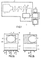
- Fig. 1 shows an imaging system, comprising an image pick-up device 2 and display means 21 and 23.
- the image pick-up device 2 comprises an image-forming unit 3, for example an image intensifier tube, endoscope or microscope with a circular exit window which forms part of an object plane 5.
- an optical system comprising a collimating lens 7, an anamorphic prism system 9 and a further lens 11, the circle situated in the object plane 5 is imaged as an ellipse on a detection face 15 of an image sensor 13.
- the anamorphic system comprises two prisms in the present embodiment, but can alternatively be formed by a system of cylindrical lenses, cylindrical mirrors or a fibre optical system.
- the image sensor 13 is, for example, a CCD sensor having a detection face 15 which is subdivided into 585 rows and 1200 columns of detection sub-faces. Via a control unit 17, a charge accumulated underneath the detection sub-faces is read and applied possibly after digital image processing in an image processing device 19, to a television monitor 21 or an image memory 23.
- Fig. 2a shows the image sensor 13, being a frame transfer CCD in the present example, which comprises a photosensitive detection face 25 and a storage section 27 which is shielded from light.
- Both sections 25 and 27 comprise, for example, n-type doped channels in a p-type substrate which extend in the vertical direction.
- Transparent polysilicon electrodes extend over the n-type channels in the horizontal direction, so that at the area where, for example, three electrodes intersect a vertical n-type channel a detection sub-face is formed having dimensions of, for example, 7.5 x 11.5 ⁇ m 2 .
- the photosensitive surface of the image sensor 13 is in the order of magnitude of 60 mm 2 .
- the detection face 25 When the detection face 25 is illuminated, positive and negative charge carriers are formed, the negative charge carriers being accumulated underneath the positive electrodes of the detection sub-faces while the positive charge carriers are dissipated to ground via the p-substrate. During a period which is within the flyback period of the television monitor 21, for example, 1.3 ms, the charge is transferred from the detection face 25 to the storage section 27.
- the control unit 17 then generates voltages across the electrodes of the detection sub-faces, the phase of said voltages differing with respect to one another in such a manner that the charge packages accumulated underneath the detection sub-faces move downwards along a column of detection sub-faces.
- the storage section 27 need only be half the size of the detection face 25.
- the charge of neighbouring rows of detection sub-faces is then summed in an alternating fashion.
- the charges are sequentially read per row of detection sub-faces at a frequency which is determined inter alia by the active line time (the time during which an image line is displayed on the television monitor 21) during display.
- the active line time amounts to approximately 52 ⁇ s; within this period, 1200 detection sub-faces must be read in the present example, so that a read frequency of read pulses generated by the control unit 17 amounts to 22.5 MHz.
- the optical system 7, 9, 11 distorts the round image so as to obtain an elliptical shape.
- the compression factor m of the optical system then equals 3 4 .
- an image displayed is composed of 625 image lines, 40 image lines being invisible, and the image frequency is 25 Hz (50 Hz 2:1 interlacing, 625/2:1/50); in accordance with the NTSC standard used in the USA, an image is composed of 525 image lines, 40 image lines of which are invisible, the image frequency being 30 Hz (60 Hz 2:1 interlacing, 525/2:1/60).
- the present ellipse 5" is situated in the centre of the detection face 25.
- the ellipse is preferably imaged so as to be tangential to the lower edge and the side of the detection face 25, so that detection sub-faces which do not contain image information are not read during the reading of the shift register 29.
- the parts of the shift register 29 which do not contain image information formed by the ellipse 5'' are preferably connected to a reset electrode 28 so that the dark current originating from the non-illuminated parts of the detection face 25 can be drained via the reset electrode.
- the reset electrode 28 may comprise a number of mutually insulated segments, which number is, for example, equal to the number of detection sub-faces in a row or may be formed by a non-interrupted metallization along the shift register 29 as shown in Fig. 2b.
- the charge of the detection sub-faces denoted by a shading can be drained by connection of the reset electrode 28 to the drain by closing a switch 26.
- the read time of the sensor is then a factor O/a.b shorter than the read time of the entire image sensor 13, where o is the non-shaded part of the detection face 25 of the image sensor 13 in Fig. 2b.
- Fig. 3 shows an image 5'' of the circular exit window situated in the object plane 5 on an image sensor 13 comprising elongate detection sub-faces when use is made of the optical system having a compression factor m equal to 1. Because of standardization it is desirable to distribute a circular image 5' between an equal number of rows and columns of detection sub-faces, so that for image display or image storage the image displayed or stored is composed of square image elements. This can be achieved by using an optical system having a compression factor m equal to b n' p a n p' , where p is the number of columns of detection sub-faces of the sensor 13 and p' is the number of columns used.
- Fig. 4a illustrates a compression where the compression factor m is greater than 1, so that the long axis of the ellipse is shifted 90° with respect to the ellipse obtained in the case of image compression as shown in Fig. 3.
- b a 3 4
- the images are stored in the line or image memory 23 and can be applied, after termination of the exposure, to the television monitor 21 with an adapted frequency, so that the circular image 5' is displayed without distortion on the television monitor.
- the output of the shift register 29 of the image sensor 13 may also be directly connected to a television monitor operating at 100 Hz. Because of a higher illumination intensity on the image sensor 13 for small values of the compression factor, the value of the compression factor m preferably remains smaller than 1 and the image sensor is preferably rotated with respect to the object plane.
- Imaging with a frequency of 100 Hz is also used in time sequential stereoscopy.
- two mutually shifted X-ray sources produce 100 X-ray images per second which are displayed on a television monitor operating at 100 Hz.
- the observer of the television monitor then wears spectacles whose glasses are alternately darkened at a frequency of 100 Hz, for example, by means of liquid crystals. Because each eye observes an image at a frequency of 50 Hz, no disturbing image flicker is observed and a stereoscopic image is obtained.
- Fig. 5 shows the television monitor 21 with a display face having a long side q and a short side r.
- the read frequency is usually fixed because read frequency synchronization signals for the television monitor must be extracted from the integer factor.
- an image sensor having an image sensor constant k1 is capable of cooperating with a television monitor having an image display constant k2.
- the compression factor is fixed by the requirement that the number of rows n' and the number of columns p' in an elliptical image 5" on the image sensor 13 must be the same and the read frequency has a given value because of the synchronization requirements imposed, it may be that fp ⁇ k1.k2 m . Consequently, the circular image 5' is displayed on the television monitor in distorted form.
- one of these requirements can be satisfied by adaptation of the compression factor.
- Fig. 6 shows an embodiment of an imaging system comprising a beam splitter 12 which cooperates with the optical system 9, 11 and two image sensors 13A and 13B.
- the beam splitter 12 images an elliptical image of the circle in the object plane 5 on the respective image sensors 13A and 13B so as to be shifted over a distance amounting to half a detection sub-face.
- the image resolution is thus doubled in the direction of shift of the two images on the sensors 13A and 13B, for example in the vertical direction.
- An image sensor A denoted by a broken line in the Figure and comprising four detection sub-faces A11 ...
- A22 is shifted over one half detection sub-face in the vertical direction with respect to an image sensor B comprising four detection sub-faces B11 ... B22.
- the centres of charge accumulation of the detection sub-faces, being situated in the centre of the detection sub-faces, can thus be doubled.
- a p now equals a dimension xp of a detection sub-face in the row direction of the image sensor and b n equals a dimension yp of a detection sub-face in the column direction of the image sensor.
- the compression factor m yp n' xp p' .
- the compression factor should be adapted in proportion.
- Fig. 8 shows an embodiment of the image processing device 19 which is connected to two image sensors 13A and 13B. Identical images which have been shifted over one half detection sub-face with respect to one another appear on the detection faces of the image sensors.
- the signals of the image sensors are simultaneously written into a memory 30 and a memory 31, respectively.
- Via a multiplexer 33 a row of signals is alternately read from the memory 30 and the memory 31 at a rate which amounts to twice the rate at which the signals of the image sensors 13A and 13B are written into the memories 30 and 31.
- the signals are applied, via a digital-to-analog converter, to a television monitor 21 on which an image appears whose resolution amounts to twice the resolution of the individual image sensors 13A and 13B.
- the switches S1 and S2 are closed, the signals of the image sensors 13A and 13B are summed. In that case no mutual image shift between the image sensors takes place.
- An image displayed has the same resolution as the image detected on the image sensors.
- Such an application is desirable, for example, in fluoroscopy where a low light intensity necessitates integration of the image information in order to obtain a suitable signal-to-noise ratio.
Description
- The invention relates to an imaging system comprising an image pick-up device with an image sensor having a detection face which is subdivided into detection sub-faces for converting a radiation intensity distribution on the detection face into an electric signal, the detection face having a rectangular shape with a long side and a short side, the detection sub-faces being arranged in a matrix of n rows and p columns, the detection sub-faces having an elongate shape, an object plane and an optical system which cooperates with the object plane and the image sensor in order to display the radiation intensity distribution on the detection face, the optical system imaging a circle situated in the object plane as an ellipse,the imaging system also comprising display means which are coupled to the image sensor in order to display the radiation intensity distribution on the detection face.
- An imaging system of the kind set forth is known from the United States Patent US-A-4 706 122.
- The optical system of the known imaging system performs an image compression which renders the known imaging system compatible with various television systems employing different aspect ratios of the entire image area. According to the cited Patent Application, a circular exit screen of an image intensifier tube is imaged, via the optical system, as an inscribed ellipse on a rectangular CCD matrix, the long and short axes of the ellipse being equal to the long side and the short side, respectively, of the CCD matrix. Thus, optimum use is made of the detection face of the CCD matrix and the resolution is enhanced in the direction of the long axis of the ellipse. The ellipse can be displayed as a circle again on a display unit by accelerated reading of the detection sub-faces of the CCD matrix in a row direction (video line direction).The known imaging system comprises an image sensor having detection sub-faces having an elongate shape, but the optical compression employed in the known imaging system is not related to the shape of the detection sub-faces. Hence, the known imaging system is not suitable to process image information originating from image sensors having detection sub-faces of different shape. In particular the known imaging system is not suitable to display image information or store image information from image sensors having differently shaped detection sub-faces without causing perturbations in the displayed or stored image information.
- An object of the invention is to provide an imaging system which generates an image that upon display or storage consists of substantially square elements.
- This object is achieved by an imaging system according to the invention which is characterized in that a short axis of the ellipse is shorter that the short side of the detection face,in the case of a long side of the detection face having a length a and a short side of the detection face having a length b, the optical imaging system images said circle as an ellipse on n' rows and p' columns of detection sub-faces, where p'≤p and n'<n and the axes of said ellipse extend along an equal number of detection sub-faces, so that axes k and l of the ellipse have a ratio k/l=bp/(an).
- When the display means comprise a cathode ray tube, the signals of the detection sub-faces are made visible on a phosphorescent display screen along the image lines. To this end, the charge accumulated, for example, underneath the detection sub-faces in a CCD image sensor of the frame transfer type, is introduced into a shift register in parallel per row of detection sub-faces, the charge being applied from said shift register to the cathode ray tube per detection sub-face. The signal value of a detection sub-face modulates the intensity of an electron beam scanning the display screen and becomes visible as a brightness variation with respect to a dark level on the display screen. The detection sub-faces are thus distributed as if it were across the display screen, the position of the detection sub-faces along an image line and the position of a row of detection sub-faces on the display screen being determined by the frequency at which the detection sub-faces are shifted out of the shift register. The number of rows of detection sub-faces of the image sensor which can be displayed on the display screen is determined by the number of lines constituting the image on the display screen. When the number of rows of detection sub-faces of the image sensor amounts to n and the number of lines of the display screen of the display means amounts to n', where n > n', not all rows of detection sub-faces can be displayed on the display screen. As a result, image compression of a round image on the image sensor into an elliptical image which covers the surface of the image sensor as well as possible, is of limited use. In such a case the optical system distorts a round image by a compression factor m, m being the ratio of the short axis of the ellipse to the long axis of the ellipse, where m =

- When the compression factor m is reduced to


- When the detection sub-faces have an elongate shape, the compression factor of the optical system is advantageously adjusted so that the axes of the ellipse extend along an equal number of detection sub-faces. Because p' = n', the compression factor m becomes m=

- Another embodiemnt of an imaging system according to the invention comprises an image pick-up device provided with a plurality of t image sensors t being at least equal to 2, each image sensor having a detection face which is subdivided into detection sub-faces for converting a radiation intensity distribution on the detection face into an electric signal, the detection sub-faces being arranged in a matrix in rows and columns, said detection sub-faces having a dimension x in a row direction and a dimension y in a column direction, an object plane and an optical system which cooperates with the object plane and the image sensors in order to image the object plane on the detection face, and the optical system imaging a circle situated in the object plane as an ellipse in the case of a rectangular detection face having a long side and a short side, the ellipse being imaged on each of the image sensors on n' rows and p' columns, the ellipse being shifted on the respective image sensors over a distance equal to l/t part of a dimension of a detection sub-face, the axes k and l of the ellipse satisfying


- The resolution can be enhanced by using several image sensors on which the object plane is imaged in mutually shifted positions. Because the effective dimension of the detection sub-faces is thus reduced, it is necessary to adapt the optical system in order to produce the correct image compression so that the image sensors can cooperate with the display means in the same way as when one image sensor is used.
- An embodiment of an imaging system in accordance with the invention is characterized in that the image sensor comprises a shift register for parallel reception of charges from detection sub-faces situated in a row and for sequential output of charges stored in the shift register to the display means, the shift register being provided, over at least a part of its length, with a reset electrode for applying charges stored in the shift register to a drain.
- When the charge of the detection sub-faces which do not contain image information is discharged via the reset electrode, the image sensor will be ready to accept a next image sooner than when all detection sub-faces are read via the shift register. This is important notably for the imaging of fast moving objects, for example pediatric X-ray imaging at a frequency of 100 Hz. As a result of the use of the reset electrode, the image information of each even row of detection sub-faces in a first image of the image sensor can be discharged to the drain and in a second image the image information of every odd row of detection sub-faces can be discharged thereto. The two images successively obtained can be displayed on the television monitor in an interlaced manner. The resolution is thus enhanced in comparison with the resolution obtained in the case of an imaging mode where the image sensor forms a first image with pair-wise combination of neighbouring rows of detection sub-faces (for example,
rows rows 3 and 4,rows 5 and 6, etc.) and where a second image is formed by pair-wise combination of neighbouring rows of detection sub-faces which have been shifted over one row with respect to the first image (for example,rows rows 4 and 5,rows 6 and 7, etc.). - Some embodiments of an imaging system in accordance with the invention will be described in detail hereinafter with reference to the accompanying drawing. Therein:
- Fig. 1 shows an imaging system in accordance with the invention;
- Fig. 2a diagrammatically shows an image sensor;
- Fig. 2b shows the detection elements of the image sensor as shown in Fig. 2a, the charge being applied to a drain via a reset electrode;
- Figs. 3 and 4 show an image of a circle in the object plane with different degrees of image compression;
- Fig. 5 shows a television monitor with an image of a circle in the object plane;
- Fig. 6 shows an imaging system for high-resolution imaging using two image sensors;
- Fig. 7 shows detection sub-faces of two mutually shifted image sensors; and
- Fig. 8 diagrammatically shows an image processing device for high-resolution images and images formed with a low light intensity.
- Fig. 1 shows an imaging system, comprising an image pick-up
device 2 and display means 21 and 23. The image pick-up device 2 comprises an image-formingunit 3, for example an image intensifier tube, endoscope or microscope with a circular exit window which forms part of anobject plane 5. Via an optical system, comprising acollimating lens 7, ananamorphic prism system 9 and afurther lens 11, the circle situated in theobject plane 5 is imaged as an ellipse on adetection face 15 of animage sensor 13. The anamorphic system comprises two prisms in the present embodiment, but can alternatively be formed by a system of cylindrical lenses, cylindrical mirrors or a fibre optical system. Theimage sensor 13 is, for example, a CCD sensor having adetection face 15 which is subdivided into 585 rows and 1200 columns of detection sub-faces. Via acontrol unit 17, a charge accumulated underneath the detection sub-faces is read and applied possibly after digital image processing in animage processing device 19, to atelevision monitor 21 or animage memory 23. - Fig. 2a shows the
image sensor 13, being a frame transfer CCD in the present example, which comprises aphotosensitive detection face 25 and astorage section 27 which is shielded from light. Bothsections image sensor 13 is in the order of magnitude of 60 mm2. When thedetection face 25 is illuminated, positive and negative charge carriers are formed, the negative charge carriers being accumulated underneath the positive electrodes of the detection sub-faces while the positive charge carriers are dissipated to ground via the p-substrate. During a period which is within the flyback period of thetelevision monitor 21, for example, 1.3 ms, the charge is transferred from thedetection face 25 to thestorage section 27. Thecontrol unit 17 then generates voltages across the electrodes of the detection sub-faces, the phase of said voltages differing with respect to one another in such a manner that the charge packages accumulated underneath the detection sub-faces move downwards along a column of detection sub-faces. When an image to be displayed on thetelevision monitor 21 is composed of frames which are each time formed by two interlaced fields, thestorage section 27 need only be half the size of thedetection face 25. The charge of neighbouring rows of detection sub-faces is then summed in an alternating fashion. Via ashift register 29, the charges are sequentially read per row of detection sub-faces at a frequency which is determined inter alia by the active line time (the time during which an image line is displayed on the television monitor 21) during display. According to the PAL television standard, the active line time amounts to approximately 52 µs; within this period, 1200 detection sub-faces must be read in the present example, so that a read frequency of read pulses generated by thecontrol unit 17 amounts to 22.5 MHz. In order to adapt the circular exit window of the image-formingunit 3, situated in theobject plane 5, to thedetection face 15, usually having an aspect ratio

television monitor 21 equal to the number of rows of detection sub-faces of theimage sensor 13, theoptical system 
image sensor 13, stronger image compression by the optical system is desirable, the compression factor m of the optical system then amounting to


- The
present ellipse 5" is situated in the centre of thedetection face 25. However, the ellipse is preferably imaged so as to be tangential to the lower edge and the side of thedetection face 25, so that detection sub-faces which do not contain image information are not read during the reading of theshift register 29. The parts of theshift register 29 which do not contain image information formed by the ellipse 5'' are preferably connected to areset electrode 28 so that the dark current originating from the non-illuminated parts of thedetection face 25 can be drained via the reset electrode. Thereset electrode 28 may comprise a number of mutually insulated segments, which number is, for example, equal to the number of detection sub-faces in a row or may be formed by a non-interrupted metallization along theshift register 29 as shown in Fig. 2b. When an ellipse is imaged on theimage sensor 13, as shown in Fig. 2b, the charge of the detection sub-faces denoted by a shading can be drained by connection of thereset electrode 28 to the drain by closing aswitch 26. Assuming that the period of time required for discharging the charge to the drain is negligibly small, the read time of the sensor is then a factor O/a.b shorter than the read time of theentire image sensor 13, where o is the non-shaded part of thedetection face 25 of theimage sensor 13 in Fig. 2b. - Fig. 3 shows an image 5'' of the circular exit window situated in the
object plane 5 on animage sensor 13 comprising elongate detection sub-faces when use is made of the optical system having a compression factor m equal to 1. Because of standardization it is desirable to distribute a circular image 5' between an equal number of rows and columns of detection sub-faces, so that for image display or image storage the image displayed or stored is composed of square image elements. This can be achieved by using an optical system having a compression factor m equal to
sensor 13 and p' is the number of columns used. Another reason for not using all available columns may reside in the read frequency of the detection sub-faces to be used. When the read frequency and the number of rows of detection sub-faces n' to be used are fixed, the number of columns of detection sub-faces to be used is defined so that p' could be unequal to n'. In the example shown in Fig. 3,


- Fig. 4a illustrates a compression where the compression factor m is greater than 1, so that the long axis of the ellipse is shifted 90° with respect to the ellipse obtained in the case of image compression as shown in Fig. 3. In the present example,


image sensor 13, enables the image to be read in half the period of time required for reading the entire surface of the image sensor via theshift register 29. The charge of the detection sub-faces of theimage sensor 13 which have not been illuminated is drained via thereset electrode 28 of theshift register 29. As a result, for a constant read frequency fp of theshift register 29, imaging on thephotosensitive portion 25 of the image sensor can be twice as fast. Using an image sensor having a read frequency adapted to 50 complete detection faces per second and to imaging according to the 625/2:1/50 format, resulting in a mean read frequency fp = 50.n.p, such image compression and image translation enable exposures to be made at 100 Hz because fp = 100.n p/2. Thus, at the same read frequency, the image sensor is suitable for imaging according to the 625/2:1/100 format. This is advantageous notably when pediatric X-ray images are formed where irradiation using X-rays with pulses of 100 Hz is desirable for the imaging of comparatively fast moving medical details. The images are stored in the line orimage memory 23 and can be applied, after termination of the exposure, to thetelevision monitor 21 with an adapted frequency, so that the circular image 5' is displayed without distortion on the television monitor. The output of theshift register 29 of theimage sensor 13 may also be directly connected to a television monitor operating at 100 Hz. Because of a higher illumination intensity on theimage sensor 13 for small values of the compression factor, the value of the compression factor m preferably remains smaller than 1 and the image sensor is preferably rotated with respect to the object plane. - Imaging with a frequency of 100 Hz is also used in time sequential stereoscopy. Therein, two mutually shifted X-ray sources produce 100 X-ray images per second which are displayed on a television monitor operating at 100 Hz. The observer of the television monitor then wears spectacles whose glasses are alternately darkened at a frequency of 100 Hz, for example, by means of liquid crystals. Because each eye observes an image at a frequency of 50 Hz, no disturbing image flicker is observed and a stereoscopic image is obtained.
- When a given compression factor is used and the circular image 5' which would appear on the
image sensor 13 when using a compression factor m equal to l is to be displayed on thetelevision monitor 21 in non-distorted form, the read frequency of the read operation controlled by the control unit should be adapted to the compression factor. Fig. 5 shows thetelevision monitor 21 with a display face having a long side q and a short side r. The circular image 5' of the image sensor, distorted by a compression factor m by theoptical system shift register 29 with a read frequency fp. During the active line time Tl of the television monitor, amounting to, for example 52 µs, an image line contains image information only over the length l. As a result, an effective line time Te of thetelevision monitor 21 becomes: Tle = T .
television monitor 21 is composed of z image lines,
image sensor 13, so that:

shift register 29 amounts to fp = p'/Tle within the effective line time. Substitution of the previously found effective line time in the latter relation results in a read frequency fp =


- The read frequency is usually fixed because read frequency synchronization signals for the television monitor must be extracted from the integer factor. By using a correct compression factor, an image sensor having an image sensor constant k1 is capable of cooperating with a television monitor having an image display constant k2. When the compression factor is fixed by the requirement that the number of rows n' and the number of columns p' in an
elliptical image 5" on theimage sensor 13 must be the same and the read frequency has a given value because of the synchronization requirements imposed, it may be that fp ≠
- Fig. 6 shows an embodiment of an imaging system comprising a
beam splitter 12 which cooperates with theoptical system image sensors 13A and 13B. Thebeam splitter 12 images an elliptical image of the circle in theobject plane 5 on therespective image sensors 13A and 13B so as to be shifted over a distance amounting to half a detection sub-face. The image resolution is thus doubled in the direction of shift of the two images on thesensors 13A and 13B, for example in the vertical direction. This is illustrated in Fig. 7. An image sensor A, denoted by a broken line in the Figure and comprising four detection sub-faces A11 ... A22, is shifted over one half detection sub-face in the vertical direction with respect to an image sensor B comprising four detection sub-faces B11 ... B22. The centres of charge accumulation of the detection sub-faces, being situated in the centre of the detection sub-faces, can thus be doubled. When several, mutually shifted image sensors are used, it is necessary to adapt the compression factor of theoptical system 


- Fig. 8 shows an embodiment of the
image processing device 19 which is connected to twoimage sensors 13A and 13B. Identical images which have been shifted over one half detection sub-face with respect to one another appear on the detection faces of the image sensors. The signals of the image sensors are simultaneously written into amemory 30 and amemory 31, respectively. Via amultiplexer 33, a row of signals is alternately read from thememory 30 and thememory 31 at a rate which amounts to twice the rate at which the signals of theimage sensors 13A and 13B are written into thememories image processing unit 35, serving to impart a circular shape to the elliptical image of theobject plane 5, the signals are applied, via a digital-to-analog converter, to atelevision monitor 21 on which an image appears whose resolution amounts to twice the resolution of theindividual image sensors 13A and 13B. When the switches S1 and S2 are closed, the signals of theimage sensors 13A and 13B are summed. In that case no mutual image shift between the image sensors takes place. An image displayed has the same resolution as the image detected on the image sensors. Such an application is desirable, for example, in fluoroscopy where a low light intensity necessitates integration of the image information in order to obtain a suitable signal-to-noise ratio.
Claims (9)
- An imaging system (1) comprising- an image pick-up device (2) with an image sensor (13) having a detection face (25) which is subdivided into detection sub-faces for converting a radiation intensity distribution on the detection face into an electric signal,- the detection face having a rectangular shape with a long side and a short side,- the detection sub-faces being arranged in a matrix of n rows and p columns,- the detection sub-faces having an elongate shape,- an object plane (5) and an optical system (9,11) which cooperates with the object plane and the image sensor in order to display the radiation intensity distribution on the detection face,- the optical system imaging a circle situated in the object plane as an ellipse,- the imaging system also comprising display means which are coupled to the image sensor in order to display the radiation intensity distribution on the detection face,characterized in that- a short axis of the ellipse is shorter that the short side of the detection face,- in the case of a long side of the detection face having a length a and a short side of the detection face having a length b, the optical imaging system images said circle as an ellipse on n' rows and p' columns of detection sub-faces, where p'≤p and n'<n and the axes of said ellipse extend along an equal number of detection sub-faces, so that axes k and l of the ellipse have a ratio k/l=bp/(an).
- An imaging system, comprising- an image pick-up device provided with- a plurality of t image sensors (13A,13B) t being at least equal to 2,- each image sensor having a detection face which is subdivided into detection sub-faces (A11,...,A22,B11,...,B22) for converting a radiation intensity distribution on the detection face into an electric signal,- the detection sub-faces being arranged in a matrix in rows and columns,- said detection sub-faces having a dimension x in a row direction and a dimension y in a column direction,- an object plane (5) and an optical system (9,11,12) which cooperates with the object plane and the image sensors in order to image the object plane on each detection face, and the optical system imaging a circle situated in the object plane as an ellipse,- the ellipse being imaged on each of the image sensors on n' rows and p' columns,- the ellipse being shifted on the respective image sensors over a distance equal to l/t part of a dimension of a detection sub-face, the axes k and l of the ellipse satisfying


 - the imaging system further comprising display means (21) which are connected to the image sensor in order to display the radiation intensity distribution on each detection face.
 - An imaging system as claimed in Claim 2, characterized in that the short axis of the ellipse is shorter than the short side of the detection face.
- An imaging system as claimed in Claim 2 or 3, characterized in that the long axis of the ellipse is shorter than the long side of the detection face.
- An imaging system as claimed in Claim 2, 3 or 4, characterized in that the number of rows n' is equal to the number of columns p'.
- An imaging system as claimed in any one of the preceding Claims,
characterized in that- the or each image sensor comprises a shift register (29) for parallel reception of charges from detection sub-faces situated in a row and for sequential output of charges stored in the shift register to the display means,- the shift register (29) being provided, over at least a part of its length, with a reset electrode (28) for applying charges stored in the shift register to a drain. - An imaging system as claimed in Claim 6, characterized in that the shift register (29) comprises at least two mutually insulated reset electrodes (28).
- An imaging system as claimed in any one of the preceding Claims, characterized in that the optical system (9,11,12) comprises an anamorphic system (9).
- An imaging system as claimed in any one of the preceding Claims, in which the image pick-up device comprises an X-ray image intensifier tube (3) having a circular exit window which cooperates with the or each image sensor.
Applications Claiming Priority (2)
| Application Number | Priority Date | Filing Date | Title |
|---|---|---|---|
| NL9001750 | 1990-08-02 | ||
| NL9001750A NL9001750A (en) | 1990-08-02 | 1990-08-02 | IMAGE SYSTEM. |
Publications (2)
| Publication Number | Publication Date |
|---|---|
| EP0469678A1 EP0469678A1 (en) | 1992-02-05 |
| EP0469678B1 true EP0469678B1 (en) | 1997-01-29 |
Family
ID=19857504
Family Applications (1)
| Application Number | Title | Priority Date | Filing Date |
|---|---|---|---|
| EP91201960A Expired - Lifetime EP0469678B1 (en) | 1990-08-02 | 1991-07-26 | Image pick-up system with optical image shape conversion |
Country Status (5)
| Country | Link |
|---|---|
| US (1) | US5216512A (en) |
| EP (1) | EP0469678B1 (en) |
| JP (1) | JPH04256293A (en) |
| DE (1) | DE69124436T2 (en) |
| NL (1) | NL9001750A (en) |
Families Citing this family (25)
| Publication number | Priority date | Publication date | Assignee | Title |
|---|---|---|---|---|
| EP0506177A3 (en) * | 1991-03-25 | 1993-01-20 | N.V. Philips' Gloeilampenfabrieken | Television pick-up and display system, and television pick-up device and optical system suitable for use in such a system |
| EP0547679B1 (en) * | 1991-12-19 | 1996-09-04 | Koninklijke Philips Electronics N.V. | X-ray imaging system including brightness control |
| US5408265A (en) * | 1992-02-07 | 1995-04-18 | Olympus Optical Co., Ltd. | Electronic endoscope system adaptable to different T.V. standards while utilizing a common light source |
| JPH0630420A (en) * | 1992-05-13 | 1994-02-04 | Olympus Optical Co Ltd | Face sequential type image pickup device |
| WO1994018789A1 (en) * | 1993-02-11 | 1994-08-18 | Polycom, Inc. | Resolution enhancement system |
| JP3088591B2 (en) * | 1993-06-17 | 2000-09-18 | 松下電器産業株式会社 | Solid-state imaging device and driving method |
| US6721009B1 (en) * | 1994-11-12 | 2004-04-13 | Sony Corporation | Method of driving solid state imaging device |
| US5940049A (en) * | 1995-10-23 | 1999-08-17 | Polycom, Inc. | Remote interactive projector with image enhancement |
| IL135571A0 (en) * | 2000-04-10 | 2001-05-20 | Doron Adler | Minimal invasive surgery imaging system |
| US6692430B2 (en) * | 2000-04-10 | 2004-02-17 | C2Cure Inc. | Intra vascular imaging apparatus |
| DE10020261C2 (en) * | 2000-04-25 | 2003-04-17 | Rainer Mockler | Digital camera or digital video camera and image capturing method |
| EP1421775A4 (en) * | 2001-06-28 | 2009-12-23 | Given Imaging Ltd | In vivo imaging device with a small cross sectional area and methods for construction thereof |
| CA2469773A1 (en) * | 2001-12-11 | 2003-07-03 | C2Cure Inc. | Apparatus, method and system for intravascular photographic imaging |
| WO2003098913A2 (en) * | 2002-05-16 | 2003-11-27 | Cbyond Inc. | Miniature camera head |
| US7300397B2 (en) * | 2004-07-29 | 2007-11-27 | C2C Cure, Inc. | Endoscope electronics assembly |
| US20060055807A1 (en) * | 2004-09-14 | 2006-03-16 | Pemer Frederick A | Imaging methods, image sensors, imaging systems, and articles of manufacture |
| US20060221218A1 (en) * | 2005-04-05 | 2006-10-05 | Doron Adler | Image sensor with improved color filter |
| US20090046171A1 (en) * | 2007-08-16 | 2009-02-19 | C2Cure, Inc. | Non-linear color correction |
| JP4987790B2 (en) * | 2008-04-15 | 2012-07-25 | オリンパスメディカルシステムズ株式会社 | Imaging device |
| US9060674B2 (en) * | 2012-10-11 | 2015-06-23 | Karl Storz Imaging, Inc. | Auto zoom for video camera |
| US9257763B2 (en) | 2013-07-02 | 2016-02-09 | Gyrus Acmi, Inc. | Hybrid interconnect |
| US9510739B2 (en) * | 2013-07-12 | 2016-12-06 | Gyrus Acmi, Inc. | Endoscope small imaging system |
| US10606062B2 (en) * | 2018-06-20 | 2020-03-31 | Karl Storz Imaging, Inc. | Medical imaging device with split image on common image sensor |
| US11497389B2 (en) | 2018-10-03 | 2022-11-15 | Karl Storz Imaging, Inc. | Attachment system for conditioning light between endoscope and camera |
| US11586029B2 (en) | 2020-12-09 | 2023-02-21 | Karl Storz Imaging, Inc. | Medical imaging device with split image on common image sensor |
Family Cites Families (5)
| Publication number | Priority date | Publication date | Assignee | Title |
|---|---|---|---|---|
| GB2097220B (en) * | 1981-04-16 | 1985-05-15 | Bosch Gmbh Robert | A method for the television scanning of films |
| US4706122A (en) * | 1984-08-30 | 1987-11-10 | Nec Corporation | Solid-state imaging device compatible with different television systems |
| DE3626532A1 (en) * | 1986-08-06 | 1988-02-11 | Siemens Ag | X-ray diagnosis device having a matrix of optoelectronic sensors |
| NL8701169A (en) * | 1987-05-15 | 1988-12-01 | Philips Nv | IMAGE RECORDING AND DISPLAY SYSTEM AND IMAGE RECORDING DEVICES FOR THIS. |
| EP0419118B1 (en) * | 1989-09-14 | 1995-07-12 | Sony Corporation | Charge coupled device imager with horizontal charge transfer sections in an imaging section |
-
1990
- 1990-08-02 NL NL9001750A patent/NL9001750A/en not_active Application Discontinuation
-
1991
- 1991-07-26 DE DE69124436T patent/DE69124436T2/en not_active Expired - Fee Related
- 1991-07-26 EP EP91201960A patent/EP0469678B1/en not_active Expired - Lifetime
- 1991-07-30 JP JP3190262A patent/JPH04256293A/en active Pending
- 1991-07-31 US US07/738,394 patent/US5216512A/en not_active Expired - Fee Related
Also Published As
| Publication number | Publication date |
|---|---|
| DE69124436T2 (en) | 1997-07-24 |
| JPH04256293A (en) | 1992-09-10 |
| DE69124436D1 (en) | 1997-03-13 |
| US5216512A (en) | 1993-06-01 |
| EP0469678A1 (en) | 1992-02-05 |
| NL9001750A (en) | 1992-03-02 |
Similar Documents
| Publication | Publication Date | Title |
|---|---|---|
| EP0469678B1 (en) | Image pick-up system with optical image shape conversion | |
| US4199785A (en) | Electronic zoom system | |
| EP0374253B1 (en) | Three-dimensional imaging device | |
| US4706122A (en) | Solid-state imaging device compatible with different television systems | |
| US4748507A (en) | Solid state imaging device having means to shift the image between scans and associated circuitry to improve the scanned image | |
| EP0645659A2 (en) | Three dimensional imaging apparatus, camera, and microscope. | |
| EP0289182A2 (en) | Imaging system | |
| EP0295728B1 (en) | Picture pick-up and display system and picture pick-up device suitable for said system | |
| EP0599470B1 (en) | Panoramic camera systems | |
| DE19816003C2 (en) | Method for correcting the gray values of images from a digital infrared camera | |
| US3113180A (en) | Composite image reproducing means | |
| DE3026359C2 (en) | X-ray diagnostic device with a solid-state image converter | |
| US5877807A (en) | Optoelectronic colored image converter | |
| Nakamura et al. | Recent progress of CMD imaging | |
| EP0498662B1 (en) | A method of reading out signals for a solid-state imaging device | |
| KR19980070140A (en) | Solid state image pickup device and image pickup device using the same | |
| JPS6043704B2 (en) | solid-state imaging device | |
| US5187584A (en) | X-ray fluoroscopic apparatus using a solid-state imaging device | |
| EP0701767B1 (en) | X-ray device | |
| US4644398A (en) | Superinterlacing imaging systems | |
| US4606064A (en) | Radiodiagnostic system with a flat picture intensifier | |
| JPS61172488A (en) | Solid-state image pickup device | |
| GB2253978A (en) | Raster scan system without flyback | |
| JP2003008994A (en) | Receiver | |
| EP0223281B1 (en) | Method for processing picture information having a large dynamic range with a television camera tube, and also a device for applying the method |
Legal Events
| Date | Code | Title | Description |
|---|---|---|---|
| PUAI | Public reference made under article 153(3) epc to a published international application that has entered the european phase |
Free format text: ORIGINAL CODE: 0009012 |
|
| AK | Designated contracting states |
Kind code of ref document: A1 Designated state(s): DE FR GB |
|
| 17P | Request for examination filed |
Effective date: 19920727 |
|
| 17Q | First examination report despatched |
Effective date: 19941220 |
|
| GRAG | Despatch of communication of intention to grant |
Free format text: ORIGINAL CODE: EPIDOS AGRA |
|
| GRAH | Despatch of communication of intention to grant a patent |
Free format text: ORIGINAL CODE: EPIDOS IGRA |
|
| GRAH | Despatch of communication of intention to grant a patent |
Free format text: ORIGINAL CODE: EPIDOS IGRA |
|
| GRAA | (expected) grant |
Free format text: ORIGINAL CODE: 0009210 |
|
| AK | Designated contracting states |
Kind code of ref document: B1 Designated state(s): DE FR GB |
|
| REF | Corresponds to: |
Ref document number: 69124436 Country of ref document: DE Date of ref document: 19970313 |
|
| ET | Fr: translation filed | ||
| PLBE | No opposition filed within time limit |
Free format text: ORIGINAL CODE: 0009261 |
|
| STAA | Information on the status of an ep patent application or granted ep patent |
Free format text: STATUS: NO OPPOSITION FILED WITHIN TIME LIMIT |
|
| 26N | No opposition filed | ||
| REG | Reference to a national code |
Ref country code: FR Ref legal event code: CD |
|
| PGFP | Annual fee paid to national office [announced via postgrant information from national office to epo] |
Ref country code: GB Payment date: 19990723 Year of fee payment: 9 |
|
| PGFP | Annual fee paid to national office [announced via postgrant information from national office to epo] |
Ref country code: FR Payment date: 19990727 Year of fee payment: 9 |
|
| PGFP | Annual fee paid to national office [announced via postgrant information from national office to epo] |
Ref country code: DE Payment date: 19990826 Year of fee payment: 9 |
|
| PG25 | Lapsed in a contracting state [announced via postgrant information from national office to epo] |
Ref country code: GB Free format text: LAPSE BECAUSE OF NON-PAYMENT OF DUE FEES Effective date: 20000726 |
|
| GBPC | Gb: european patent ceased through non-payment of renewal fee |
Effective date: 20000726 |
|
| PG25 | Lapsed in a contracting state [announced via postgrant information from national office to epo] |
Ref country code: FR Free format text: LAPSE BECAUSE OF NON-PAYMENT OF DUE FEES Effective date: 20010330 |
|
| REG | Reference to a national code |
Ref country code: FR Ref legal event code: ST |
|
| PG25 | Lapsed in a contracting state [announced via postgrant information from national office to epo] |
Ref country code: DE Free format text: LAPSE BECAUSE OF NON-PAYMENT OF DUE FEES Effective date: 20010501 |