EP0463594B1 - Fiber optic gyro - Google Patents
Fiber optic gyro Download PDFInfo
- Publication number
- EP0463594B1 EP0463594B1 EP91110363A EP91110363A EP0463594B1 EP 0463594 B1 EP0463594 B1 EP 0463594B1 EP 91110363 A EP91110363 A EP 91110363A EP 91110363 A EP91110363 A EP 91110363A EP 0463594 B1 EP0463594 B1 EP 0463594B1
- Authority
- EP
- European Patent Office
- Prior art keywords
- pulse
- pulses
- phase modulation
- signal
- phase
- Prior art date
- Legal status (The legal status is an assumption and is not a legal conclusion. Google has not performed a legal analysis and makes no representation as to the accuracy of the status listed.)
- Expired - Lifetime
Links
Images




Classifications
-
- G—PHYSICS
- G01—MEASURING; TESTING
- G01C—MEASURING DISTANCES, LEVELS OR BEARINGS; SURVEYING; NAVIGATION; GYROSCOPIC INSTRUMENTS; PHOTOGRAMMETRY OR VIDEOGRAMMETRY
- G01C19/00—Gyroscopes; Turn-sensitive devices using vibrating masses; Turn-sensitive devices without moving masses; Measuring angular rate using gyroscopic effects
- G01C19/58—Turn-sensitive devices without moving masses
- G01C19/64—Gyrometers using the Sagnac effect, i.e. rotation-induced shifts between counter-rotating electromagnetic beams
- G01C19/72—Gyrometers using the Sagnac effect, i.e. rotation-induced shifts between counter-rotating electromagnetic beams with counter-rotating light beams in a passive ring, e.g. fibre laser gyrometers
- G01C19/726—Phase nulling gyrometers, i.e. compensating the Sagnac phase shift in a closed loop system
Definitions
- the present invention relates to a fiber optic gyro in which a clockwise propagating light ray and a counterclockwise propagating light ray are entered into a loop-shaped optical fiber coil and, by taking advantage that a phase difference is caused between said clockwise and counterclockwise propagating light rays according to an input angular rate applied to the optical fiber coil, the input angular rate is detected.
- the invention relates to such a portion that modulates the phases of said clockwise and counterclockwise propagating light rays so as to make a phase difference between said clockwise and counterclockwise propagating light rays alternately take + ⁇ /2 radian and - ⁇ /2 radian with an input angular rate of zero, while synchronizing such a phase modulation signal as described above with a light propagation time in the optical fiber coil.
- Fig. 1 shows an example of a conventional fiber optic gyro.
- a light beam emitted from a light source 1 is entered into a beam splitter 13 via a beam splitter 12.
- the light beam is split into two rays by the beam splitter 13 and entered into an optical transmission path (i.e., an optical fiber coil) 14 as a clockwise propagating light ray and a counterclockwise propagating light ray.
- the clockwise propagating light ray is entered into the optical fiber coil 14 via a phase modulator 15.
- the clockwise light ray leaves the optical fiber coil 14 and is transmitted through a biasing phase modulator 16 and then returns to the beam splitter 13.
- the counterclockwise light ray is transmitted into the phase modulator 16 from the beam splitter 13, then proceeds to the optical fiber coil 14 and, after that, it enters the beam splitter 13 via the phase modulator 15 where the counterclockwise light ray is combined with the clockwise light ray while causing interference therebetween.
- combined interference light beam is entered into the beam splitter 12 from which the beam propagates to an opto-electric converter 17 where the beam is converted to an electric signal FR representing the intensity of the combined light (interference light).
- the relative phase difference between the clockwise light and the counterclockwise light, after returning to the beam splitter 13, is 0 unless the optical fiber coil 14 revolves around an axial center thereof.
- an irreversible phase shift is created between the clockwise light and the counterclockwise light owing to the Sagnac effect while resulting in a change of the intensity of the combined light (interference light) detected by the opto-electric converter 17, because of said phase shift.
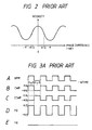
- Said phase difference and the change in the intensity of the combined light (interference light) takes a relationship as shown in Fig. 2 as represented by a sine function.
- a phase modulation signal BPM in a rectangular wave with a period of 2T is generated from a phase modulation signal generator 18.
- a biasing phase modulator 16 is thereby activated to give phase shifts of ⁇ /4 radian and - ⁇ /4 radian alternately in light signals.
- the time interval T is made equal to a light propagation time ⁇ through the optical fiber coil 14. Therefore, as shown in Rows B and C of Fig.
- the output FR of the opto-electric converter 17 is amplified by an amplifier 19 while an amplified output thereof being synchronously detected by an output of a phase modulation signal generator 18 in a synchronous detector 21.
- the synchronous detector 21 issues an output signal that shows a magnitude and a direction of a phase shift in relation to the bias phase modulation signal BPM.
- Said output signal is integrated in an integrator 22 while supplying an integrated output thereof to a ramp voltage generator 23 which issues a ramp signal output in a slope and a polarity according to the input thereto.
- Said ramp signal output activates the phase modulator 15 that generates such a phase difference as to cancel the phase difference induced owing to the Sagnac effect between the clockwise light and the counterclockwise light.
- the magnitude and direction of the input angular rate are obtained.
- phase modulations CWP and CCWP shown in Rows B and C of Fig. 3B effected to both light rays returned to the beam splitter 13 take such a relationship that the phase of the counterclockwise light lags by T ( ⁇ radians) or more from that of the clockwise light. Therefore, the phase difference PD between these light rays becomes zero in between ⁇ /2 radian and - ⁇ /2 radian.
- the output FR of the opto-electric converter 17 becomes maximum pulses, as revealed from the output-phase difference curve of Fig. 2.
- phase modulations CWP and CCWP received by both light rays returned to the beam splitter 13 are such that the counterclockwise light lags by T ( ⁇ radian) or less from the clockwise light.
- the phase difference between both light rays becomes zero in between ⁇ /2 radian and - ⁇ /2 radian, causing maximum pulses to occur as the output FR of the opto-electric converter 17.
- the bias phase modulation signal BPM was generated by the phase modulation signal generator 18 using an output from the voltage controlled oscillator 24.
- the output from the amplifier 19 and the bias phase modulation signal BPM of the phase modulation signal generator 18 were supplied to the detector 25.
- a compensation was effected by detecting what timing a pulse generated in the output of the photo electric converter 17 occurred at in relation to an edge of the bias phase modulation signal.
- the frequency band of the photo-electric converter 17 is not always enough. Therefore, the output pulse of the opto-electric converter 17 may be subjected to waveform distortion or delay, causing an error in a relative timing with the phase modulation signal while making it difficult to precisely compensate the time interval T.
- the document WO-A-89-07237 discloses a closed loop fiber optic gyroscope in which two complementary triangular phase modulation signals are applied to two phase modulators provided at opposite ends of the optical fiber coil, thereby to achieve a basing phase modulation and, at the same time, a closed loop operation by skewing the triangular waveform in such a way as to compensate for any rotation induced phase difference.
- the triangular waveform may be a stepped waveform which, when the gyroscope is not subjected to rotation is symmetric but becomes asymmetric as soon as a rotation induced phase difference occurs.
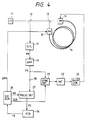
- Fig. 4 shows an embodiment of the present invention depicting parts corresponding to those shown in Fig. 1 using the same numerals.
- Said phase modulation signal BPM actuates a biasing phase modulator 16.
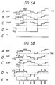
- the signal generator 26 generates a rectangular reference signal SQR in synchronization with a phase difference signal PD between both light rays as shown in Fig. 5A, in a period of 2nT, with which an output PS of an amplifier 19 is synchronously detected in a synchronous detection circuit 21.
- T ⁇ with a zero input angular rate
- an output FR from the opto-electric converter 17 takes a stationary level as shown in Row E of Fig. 5A, in the same manner as known in the prior art.
- phase modulation CCWP received by the counterclockwise light lags from a phase modulation CWP received by the clockwise light returned to the beam splitter 13, by T + ⁇ T. Consequently, the phase difference PD between both light rays mainly take ⁇ /2 radian in a section where phase modulations CWP and CCWP repeat the steps of + ⁇ /2 radian (increasing section). However, there are such sections ⁇ T where the phase difference PD becomes ⁇ radians at every T.
- the PD mainly takes - ⁇ /2 radian with such a section ⁇ T where it becomes - ⁇ /2 radian every T.
- a section where a phase difference and a length are zero and ⁇ T respectively.
- the output FR of the opto-electric converter 17 takes maximum, minimum and a stationary value when the phase difference is zero, ⁇ and ⁇ /2, respectively.
- negative-going pulses are created in the output FR of the opto-electric converter 17 in the increasing and decreasing sections as shown in Row E of Fig. 5B.
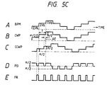
- phase modulation CCWP received by the counterclockwise light lags by T - ⁇ T from the phase modulation CWP received by the clockwise light returned to the beam splitter 13 with a zero input angular rate, as shown in Fig. 5C.
- Phase differences PD of both light rays mainly take ⁇ /2 radian in an increasing section but such a section where a phase difference and a time length thereof are zero and ⁇ T, respectively is repeated every T.
- phase differences PD mainly take - ⁇ /2 radian but the section of a zero phase difference and a ⁇ T length is repeated every T. Therefore, such a pulse of ⁇ T in width taking a maximum level every T is created. More explicitly, as shown in Row E of Fig. 5C, a positive-going pulse is created in either an increasing or a decreasing section.
- a pulse detector 27 it is detected using a pulse detector 27 whether there is either a negative-going pulse or a positive-going pulse in an increasing or decreasing section of the biasing phase modulation signal BPM. If a negative-going pulse is detected, a voltage controlled oscillator 24 is controlled to have no negative-going pulse generated as detection output. That is, an oscillation frequency of the voltage controlled oscillator 24 is made lower. When a positive-going pulse is detected, the voltage controlled oscillator 24 is controlled accordingly so that no positive-going pulses are generated. That is, an oscillation frequency of the voltage controlled oscillator 24 is made higher.
- the pulse detector 27 can be composed as shown in Fig. 6 for example. More explicitly, an output PS of the amplifier 19 in Fig. 4 is supplied to a non-inverting input terminal of a comparator 31 and a inverting input terminal of a comparator 32, from a terminal 28 after cutting off DC by a capacitor 29. As shown in an operation time chart of Fig. 7, an input signal PS to the terminal 28 is DC-filtered corresponding to ⁇ /2 radian and - ⁇ /2 radian and then compared to voltages +V m and -V m in the comparators 31, 32. The voltages +V m and -V m are provided to prevent error operations owing to a phase difference caused by the Sagnac effect.
- the absolute value of said voltages is made larger than the absolute value of an output corresponding to a phase difference caused by an expected steep angular rate input.
- a positive-going pulse is detected by the comparator 31 while detecting a negative-going pulse in the comparator 32.
- the width of an output pulse from the comparator 31 or 32 is made constant, if so required, in a oneshot circuit 33 or 34 while supplying the output pulse to a gate 35 or 36.
- a window signal WS is supplied from the signal generator 26 to gates 35, 36 to take out pulses in an increasing section and decreasing section for the biasing phase modulation signal BPM, while blocking pulses generated at a transition portion between an increasing section and a decreasing section.
- Output pulses from the gate 35 are up-counted in a counter 37 while down-counting output pulses from the gate 36 in the counter 37.
- the counter 37 down-counts in the zero state, it counts -1, -2, -3, ---.
- a value counted by the counter 37 is converted to an analog signal by a DA converter 38. Said analog signal is added to a reference signal Vr in an adder 39 as a compensation signal.
- An output VS from the adder 39 is supplied to the voltage controlled oscillator (VSO) 24 as a control signal.
- VSO voltage controlled oscillator
- a negative-going pulse is created in the output PS of the amplifier 19. Said pulse is down-counted in the counter 37 providing a certain negative value as a counting of the counter 37.
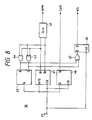
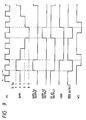
- a signal FS of a period T issued from the voltage controlled oscillator 24 is given to a clock terminal CK of the up-down counter 41 while giving a counted value "Q1Q0" thereof to the D-A converter 42.
- the D-A converter 42 issues analog voltages zero, V( ⁇ /2), V( ⁇ ) and V(3 ⁇ /2) with input values "Q1Q0" of "00", "01", "10” and "11” respectively.
- Said voltages provide the clockwise light and the counterclockwise light with phase shifts of zero, ⁇ /2, ⁇ and 3 ⁇ /2 radians, respectively.
- a counted value Q1Q0 of the counter 41 is applied to a NOR gate 43 and a AND gate 44, the outputs of which are given to a set terminal S and a reset terminal R of a flip-flop 45, respectively.
- the flip-flop 45 is set only with the counted value "Q1Q0" of "00", while being reset only with a counted value "Q1Q0" of "11". With values other than the above, the flip-flop maintains a previous state.
- the up-down counter 41 up-counts pulses of an input signal FS when the Q output of the flip-flop 45 is in a high level, while down-counting with a Q output in a low level. Consequently, when a counted value "Q1Q0" of the counter 41 becomes "00", the counter 41 enters an up-count mode, in which the voltage of the phase modulation signal BPM, an output of the DA converter 42, steps up every period of T as shown in Fig. 9 in order to sequentially up-count pulses of the input signal FS.
- the flip-flop 45 When a counted value "Q1Q0" thereof arrives at "11", the flip-flop 45 is reset to set the counter 41 in a down-count mode in which pulses of the input signal FS are sequentially down-counted. Therefore, the voltage of BPM, an output of the DA converter 42, steps down every period of T.
- the flip-flop 46 reads said Q output in the period T of the input signal FS, the same waveform as the Q output waveform of the flip-flop 45 is obtained in the Q output, in a phase delayed by the period T.
- the Q output of the flip-flop 46 is applied to the synchronous detector 21 as a reference signal SQR.
- the outputs of the gates 43 and 44 are entered into an XOR gate 47.
- An output from said gate 47 is such a signal waveform that a level thereof becomes low level in a period when a reset signal and a set signal are given to the flip-flop 45 while becoming high level in other periods.
- Said signal waveform is read into the flip-flop 48 by a reversed pulse of the input signal FS, so a waveform obtained at the Q output is such that the output waveform of the XOR gate 47 is delayed by T/2.
- the waveform thus delayed forms a window signal WS whose level becomes low only during a period T with a center of either a rise edge for the waveform of the phase modulation signal BPM to begin increasing or a fall edge for the same to begin decreasing.
- the phase modulation signal in use is such that the increasing of a magnitude giving a phase shift of ⁇ /2 radian every time interval T is repeated for n steps and then the decreasing of a magnitude to give a phase shift of ⁇ /2 radian every time interval T is repeated n steps.
- it is detected whether there is either a positive-going pulse or a negative-going pulse. If there is a positive-going pulse, the time interval T is shortened accordingly in order that positive-going pulses no longer occur. When there is a negative-going pulse, the time interval T is shortened correspondingly so that negative-going pulses disappear.
- the method of the present invention is unlike conventional systems where a relative timing of pulses is detected to determine whether the pulses are leading or lagging from an edge of the phase modulation signal. But, the invented method is to discriminate whether a pulse is positive or negative going one. Therefore, the novel system can make the time interval T precisely in agreement with the propagation time ⁇ no matter whether the waveform of pulses is distorted or the timing thereof is delayed because the frequency band of the opto-electric converter 17 is not wide enough.
Landscapes
- Engineering & Computer Science (AREA)
- Physics & Mathematics (AREA)
- Power Engineering (AREA)
- Optics & Photonics (AREA)
- Electromagnetism (AREA)
- General Physics & Mathematics (AREA)
- Radar, Positioning & Navigation (AREA)
- Remote Sensing (AREA)
- Gyroscopes (AREA)
Description
- The present invention relates to a fiber optic gyro in which a clockwise propagating light ray and a counterclockwise propagating light ray are entered into a loop-shaped optical fiber coil and, by taking advantage that a phase difference is caused between said clockwise and counterclockwise propagating light rays according to an input angular rate applied to the optical fiber coil, the input angular rate is detected. More particularly, the invention relates to such a portion that modulates the phases of said clockwise and counterclockwise propagating light rays so as to make a phase difference between said clockwise and counterclockwise propagating light rays alternately take +π/2 radian and -π/2 radian with an input angular rate of zero, while synchronizing such a phase modulation signal as described above with a light propagation time in the optical fiber coil.
- Fig. 1 shows an example of a conventional fiber optic gyro. A light beam emitted from a
light source 1 is entered into abeam splitter 13 via abeam splitter 12. The light beam is split into two rays by thebeam splitter 13 and entered into an optical transmission path (i.e., an optical fiber coil) 14 as a clockwise propagating light ray and a counterclockwise propagating light ray. At that time, the clockwise propagating light ray is entered into theoptical fiber coil 14 via aphase modulator 15. The clockwise light ray leaves theoptical fiber coil 14 and is transmitted through abiasing phase modulator 16 and then returns to thebeam splitter 13. The counterclockwise light ray is transmitted into thephase modulator 16 from thebeam splitter 13, then proceeds to theoptical fiber coil 14 and, after that, it enters thebeam splitter 13 via thephase modulator 15 where the counterclockwise light ray is combined with the clockwise light ray while causing interference therebetween. Thus again combined interference light beam is entered into thebeam splitter 12 from which the beam propagates to an opto-electric converter 17 where the beam is converted to an electric signal FR representing the intensity of the combined light (interference light). - In a fiber optic gyro, the relative phase difference between the clockwise light and the counterclockwise light, after returning to the
beam splitter 13, is 0 unless theoptical fiber coil 14 revolves around an axial center thereof. When theoptical fiber coil 14 revolves around the axial center thereof, an irreversible phase shift is created between the clockwise light and the counterclockwise light owing to the Sagnac effect while resulting in a change of the intensity of the combined light (interference light) detected by the opto-electric converter 17, because of said phase shift. Said phase difference and the change in the intensity of the combined light (interference light) takes a relationship as shown in Fig. 2 as represented by a sine function. The magnitude and direction of the change in the intensity of said interference light are detected in order to detect an input angular rate. According to the prior art, in order to have the fiber optic gyro actuated at a most sensitive operating point, for example, at the point of a phase difference of ±π/2 radian, a phase modulation signal BPM in a rectangular wave with a period of 2T is generated from a phasemodulation signal generator 18. Abiasing phase modulator 16 is thereby activated to give phase shifts of π/4 radian and -π/4 radian alternately in light signals. The time interval T is made equal to a light propagation time τ through theoptical fiber coil 14. Therefore, as shown in Rows B and C of Fig. 3A, when the clockwise light ray and the counterclockwise light ray return to thebeam splitter 13, the phases of both light rays are shifted by π/4 radian (CWP) and -π/4 radian (CCWP), respectively at the same time. Consequently, the phase difference between both light rays repeatedly becomes π/2 radian and -π/2 radian in a cycle time of T each, as shown in Row D of Fig. 3A. Obviously in Fig. 2, the sensitivity becomes maximum at phase differences of π/2 and -π/2 and, at these operating points, the interference light takes the same level of optical intensity. Therefore, the level of an output FR from the opto-electric converter 17 becomes stationary as shown in Row E of Fig. 3A. - The output FR of the opto-
electric converter 17 is amplified by anamplifier 19 while an amplified output thereof being synchronously detected by an output of a phasemodulation signal generator 18 in asynchronous detector 21. Thesynchronous detector 21 issues an output signal that shows a magnitude and a direction of a phase shift in relation to the bias phase modulation signal BPM. Said output signal is integrated in anintegrator 22 while supplying an integrated output thereof to aramp voltage generator 23 which issues a ramp signal output in a slope and a polarity according to the input thereto. Said ramp signal output activates thephase modulator 15 that generates such a phase difference as to cancel the phase difference induced owing to the Sagnac effect between the clockwise light and the counterclockwise light. At that time, by measuring the frequency and polarity of the ramp voltage signal by a means not illustrated, the magnitude and direction of the input angular rate are obtained. - If the time interval T to modulate phases is smaller than a propagation time τ through the
optical fiber coil 14 in the case where an input angular rate is zero, phase modulations CWP and CCWP shown in Rows B and C of Fig. 3B effected to both light rays returned to thebeam splitter 13 take such a relationship that the phase of the counterclockwise light lags by T (π radians) or more from that of the clockwise light. Therefore, the phase difference PD between these light rays becomes zero in between π/2 radian and -π/2 radian.
Correspondingly, the output FR of the opto-electric converter 17 becomes maximum pulses, as revealed from the output-phase difference curve of Fig. 2. When the time interval T of phase modulation is larger than the propagation time τ, phase modulations CWP and CCWP received by both light rays returned to thebeam splitter 13 are such that the counterclockwise light lags by T (π radian) or less from the clockwise light. The phase difference between both light rays becomes zero in between π/2 radian and -π/2 radian, causing maximum pulses to occur as the output FR of the opto-electric converter 17. - When the time interval T is not equal to τ as described above, pulses larger than the level at a phase difference of π/2 radian are generated as an output from the opto-
electric converter 17, as if there is an input angular rate which does not actually exist. As a result, operation error occurs. Consequently, according to conventional systems, the bias phase modulation signal BPM was generated by the phasemodulation signal generator 18 using an output from the voltage controlledoscillator 24. In addition, the output from theamplifier 19 and the bias phase modulation signal BPM of the phasemodulation signal generator 18 were supplied to thedetector 25. Thus, it was detected whether a pulse in the output FR of the opto-electric converter 17 occurred after or before a rise edge of the phase modulation signal BPM. A detected output controlled the voltage controlledoscillator 24 to make an oscillation frequency of the voltage controlledoscillator 24 lower if said pulse existed thereafter. If said pulse existed before the rise edge, the oscillation frequency of the voltage controlledoscillator 24 was made higher. Thereby, it was managed to have no pulse generated from the opto-electric converter 17, that is to make

According to a conventional fiber optic gyro as described above, in order to make a bias phase modulation switching time interval T equal to a light propagation time τ through theoptical fiber coil 14, a compensation was effected by detecting what timing a pulse generated in the output of the photoelectric converter 17 occurred at in relation to an edge of the bias phase modulation signal. However, the frequency band of the photo-electric converter 17 is not always enough. Therefore, the output pulse of the opto-electric converter 17 may be subjected to waveform distortion or delay, causing an error in a relative timing with the phase modulation signal while making it difficult to precisely compensate the time interval T. - The document WO-A-89-07237 discloses a closed loop fiber optic gyroscope in which two complementary triangular phase modulation signals are applied to two phase modulators provided at opposite ends of the optical fiber coil, thereby to achieve a basing phase modulation and, at the same time, a closed loop operation by skewing the triangular waveform in such a way as to compensate for any rotation induced phase difference. The triangular waveform may be a stepped waveform which, when the gyroscope is not subjected to rotation is symmetric but becomes asymmetric as soon as a rotation induced phase difference occurs.
- The document PROC. SPIE, vol. 719, Fiber Optic Gyros: 10th Anniversary Conference (1986), pages 101-112, discloses a closed loop fiber optic gyroscope in which, for achieving the closed loop operation, instead of a ramp, phase steps are generated at one end of the fiber optic coil with a duration approximately equal to the propagation time in order to minimize the width of the spikes generated by the finite slew rate of the steps.
- It is an object of the present invention to provide a fiber optic gyro in which a switching time interval T for a bias phase modulation can be in precise agreement with a propagation time τ.
- This object is achieved with a fiber optic gyro as claimed.
-
- Fig. 1 is a block diagram to show a conventional fiber optic gyro;
- Fig. 2 is a view to show the relationship between the phase difference of a clockwise propagating light ray and the counterclockwise propagating light ray and the output of an opto-electric converter;
- Fig. 3A is a time chart to describe an example of operation at

- Fig. 3B is a time chart to describe an example of operation at T < τ in Fig. 1;
- Fig. 3C is a time chart to describe an example of operation at T > τ in Fig. 1;
- Fig. 4 is a block diagram showing an embodiment of the present invention;
- Fig. 5A is a time chart to describe an example of operation at

- Fig. 5B is a time chart to describe an example of operation at T < τ in Fig. 4;
- Fig. 5C is a time chart to describe an example of operation at T > τ in Fig. 4;
- Fig. 6 is a block diagram to show an embodiment of the
pulse detector 27 in Fig. 4; - Fig. 7 is a time chart to show an example of operation thereof;
- Fig. 8 is a block diagram to show an embodiment of the
signal generator 26 in Fig. 4; and - Fig. 9 is a time chart to show an example of operation thereof.
- Fig. 4 shows an embodiment of the present invention depicting parts corresponding to those shown in Fig. 1 using the same numerals. In the present invention, a
signal generator 26 generates such a bias phase modulation signal BPM as being stepped up by a magnitude Vb corresponding to a phase shift of π/2 radian at every time interval T for n steps (for example, n = 3 in Figs. 5A and 5B) and then being stepped down by said magnitude Vb at every time interval T for n steps, as shown in Row A of Fig. 5A. Said phase modulation signal BPM actuates abiasing phase modulator 16. Therefore, when the time interval T is equal to a propagation time τ through anoptical fiber coil 14, a phase modulation CWP received by a clockwise light ray returned to abeam splitter 13 in the state of a zero input angular rate becomes as shown in row B of Fig. 5A, while a phase modulation CCWP received by the counterclockwise light ray delays by the time interval
- Therefore, the
signal generator 26 generates a rectangular reference signal SQR in synchronization with a phase difference signal PD between both light rays as shown in Fig. 5A, in a period of 2nT, with which an output PS of anamplifier 19 is synchronously detected in asynchronous detection circuit 21. In the case of
electric converter 17 takes a stationary level as shown in Row E of Fig. 5A, in the same manner as known in the prior art. When an angular rate is entered in this state, such a modulation as cancelling a phase difference caused by the Sagniac effect between the clockwise and counterclockwise propagating light rays is given to thephase modulator 15, thereby the input angular rate is measured. - In the case where the time interval T of the biasing phase modulation signal is smaller than the propagation time t through the
optical fiber coil 14, a phase modulation CCWP received by the counterclockwise light lags from a phase modulation CWP received by the clockwise light returned to thebeam splitter 13, by T + ΔT. Consequently, the phase difference PD between both light rays mainly take π/2 radian in a section where phase modulations CWP and CCWP repeat the steps of +π/2 radian (increasing section). However, there are such sections ΔT where the phase difference PD becomes π radians at every T. Likewise, in a section where phase modulations CWP and CCWP repeat the steps of -π/2 radian (decreasing section), the PD mainly takes -π/2 radian with such a section ΔT where it becomes -π/2 radian every T. In addition, immediately after a transition between increasing and decreasing sections, there is such a section where a phase difference and a length are zero and ΔT, respectively. The output FR of the opto-electric converter 17 takes maximum, minimum and a stationary value when the phase difference is zero, ±π and ±π/2, respectively. As a result, negative-going pulses are created in the output FR of the opto-electric converter 17 in the increasing and decreasing sections as shown in Row E of Fig. 5B. - When the time interval T is larger than the propagation time τ, the phase modulation CCWP received by the counterclockwise light lags by T - ΔT from the phase modulation CWP received by the clockwise light returned to the
beam splitter 13 with a zero input angular rate, as shown in Fig. 5C. Phase differences PD of both light rays mainly take π/2 radian in an increasing section but such a section where a phase difference and a time length thereof are zero and ΔT, respectively is repeated every T. Likewise, in a decreasing section, phase differences PD mainly take -π/2 radian but the section of a zero phase difference and a ΔT length is repeated every T. Therefore, such a pulse of ΔT in width taking a maximum level every T is created. More explicitly, as shown in Row E of Fig. 5C, a positive-going pulse is created in either an increasing or a decreasing section. - According to the present invention, therefore, it is detected using a
pulse detector 27 whether there is either a negative-going pulse or a positive-going pulse in an increasing or decreasing section of the biasing phase modulation signal BPM. If a negative-going pulse is detected, a voltage controlledoscillator 24 is controlled to have no negative-going pulse generated as detection output. That is, an oscillation frequency of the voltage controlledoscillator 24 is made lower. When a positive-going pulse is detected, the voltage controlledoscillator 24 is controlled accordingly so that no positive-going pulses are generated. That is, an oscillation frequency of the voltage controlledoscillator 24 is made higher. - The
pulse detector 27 can be composed as shown in Fig. 6 for example. More explicitly, an output PS of theamplifier 19 in Fig. 4 is supplied to a non-inverting input terminal of acomparator 31 and a inverting input terminal of acomparator 32, from a terminal 28 after cutting off DC by acapacitor 29. As shown in an operation time chart of Fig. 7, an input signal PS to the terminal 28 is DC-filtered corresponding to π/2 radian and -π/2 radian and then compared to voltages +Vm and -Vm in thecomparators
Referring to Fig. 7, a positive-going pulse is detected by thecomparator 31 while detecting a negative-going pulse in thecomparator 32. The width of an output pulse from thecomparator oneshot circuit gate signal generator 26 togates - Output pulses from the
gate 35 are up-counted in acounter 37 while down-counting output pulses from thegate 36 in thecounter 37. When thecounter 37 down-counts in the zero state, it counts -1, -2, -3, ---. A value counted by thecounter 37 is converted to an analog signal by aDA converter 38. Said analog signal is added to a reference signal Vr in an adder 39 as a compensation signal. An output VS from the adder 39 is supplied to the voltage controlled oscillator (VSO) 24 as a control signal. - In the state of T < τ, as shown in Fig. 5B and the left side of Fig. 7, a negative-going pulse is created in the output PS of the
amplifier 19. Said pulse is down-counted in thecounter 37 providing a certain negative value as a counting of thecounter 37. Corresponding to said counted value, a negative analog signal is supplied to the adder 39 making a control voltage to theVCO 24 smaller than Vr in order to lower the oscillation frequency of theVCO 24. Consequently, a time interval T becomes longer and, when
- In the state of T > τ to the contrary, as shown in Fig. 5C and the right side of Fig. 7, a positive-going pulse is created in an output PS of the
amplifier 19, and up-counted by thecounter 37 providing a certain positive value of counting by thecounter 37. According to said counted value, a positive analog signal is supplied to the adder 39 to make a control voltage to theVCO 24 larger than Vr while increasing an oscillation frequency of theVCO 24. Consequently, the time interval T is made shorter and, upon
- Fig. 8 shows a practical composition of the
signal generator 25 in case of N = 3 like Figs. 5A, 5B and 5C while indicating the operation thereof in the time chart of Fig. 9. A signal FS of a period T issued from the voltage controlledoscillator 24 is given to a clock terminal CK of the up-down counter 41 while giving a counted value "Q₁Q₀" thereof to theD-A converter 42. TheD-A converter 42 issues analog voltages zero, V(π/2), V(π) and V(3π/2) with input values "Q₁Q₀" of "00", "01", "10" and "11" respectively. Said voltages provide the clockwise light and the counterclockwise light with phase shifts of zero, π/2, π and 3π/2 radians, respectively. A counted value Q₁Q₀ of thecounter 41 is applied to a NORgate 43 and a ANDgate 44, the outputs of which are given to a set terminal S and a reset terminal R of a flip-flop 45, respectively. As a result, the flip-flop 45 is set only with the counted value "Q₁Q₀" of "00", while being reset only with a counted value "Q₁Q₀" of "11". With values other than the above, the flip-flop maintains a previous state. The up-down counter 41 up-counts pulses of an input signal FS when the Q output of the flip-flop 45 is in a high level, while down-counting with a Q output in a low level. Consequently, when a counted value "Q₁Q₀" of thecounter 41 becomes "00", thecounter 41 enters an up-count mode, in which the voltage of the phase modulation signal BPM, an output of theDA converter 42, steps up every period of T as shown in Fig. 9 in order to sequentially up-count pulses of the input signal FS. When a counted value "Q₁Q₀" thereof arrives at "11", the flip-flop 45 is reset to set thecounter 41 in a down-count mode in which pulses of the input signal FS are sequentially down-counted. Therefore, the voltage of BPM, an output of theDA converter 42, steps down every period of T. - The Q output of the flip-
flop 45 becomes a rectangular wave of a period
flop 46 reads said Q output in the period T of the input signal FS, the same waveform as the Q output waveform of the flip-flop 45 is obtained in the Q output, in a phase delayed by the period T. The Q output of the flip-flop 46 is applied to thesynchronous detector 21 as a reference signal SQR. The outputs of thegates XOR gate 47. An output from saidgate 47 is such a signal waveform that a level thereof becomes low level in a period when a reset signal and a set signal are given to the flip-flop 45 while becoming high level in other periods. Said signal waveform is read into the flip-flop 48 by a reversed pulse of the input signal FS, so a waveform obtained at the Q output is such that the output waveform of theXOR gate 47 is delayed by T/2. The waveform thus delayed forms a window signal WS whose level becomes low only during a period T with a center of either a rise edge for the waveform of the phase modulation signal BPM to begin increasing or a fall edge for the same to begin decreasing. - According to the present invention as described above, the phase modulation signal in use is such that the increasing of a magnitude giving a phase shift of π/2 radian every time interval T is repeated for n steps and then the decreasing of a magnitude to give a phase shift of π/2 radian every time interval T is repeated n steps. In an increasing section and a decreasing section of the biasing phase modulation signal, it is detected whether there is either a positive-going pulse or a negative-going pulse. If there is a positive-going pulse, the time interval T is shortened accordingly in order that positive-going pulses no longer occur. When there is a negative-going pulse, the time interval T is shortened correspondingly so that negative-going pulses disappear. The method of the present invention is unlike conventional systems where a relative timing of pulses is detected to determine whether the pulses are leading or lagging from an edge of the phase modulation signal. But, the invented method is to discriminate whether a pulse is positive or negative going one. Therefore, the novel system can make the time interval T precisely in agreement with the propagation time τ no matter whether the waveform of pulses is distorted or the timing thereof is delayed because the frequency band of the opto-
electric converter 17 is not wide enough.
Claims (4)
- A fiber optic gyro comprising:
a light source (11);
a beam splitter (13) for splitting a light beam from said light source (11) into two rays of light;
an optical fiber coil (14) into which said two rays of light are entered as a clockwise propagating light ray and a counterclockwise propagating light ray, respectively;
an interfering means (13) for making said two light rays emitted from said optical fiber coil (14), interfere with each other to provide an interference light beam;
an opto-electric converter (17) receiving said interference light beam and outputting an electric signal corresponding to the intensity of the interference light beam;
an optical phase modulator (16) inserted between one end of said optical fiber coil and said beam splitter and electrically controlled to shift the optical phase of light passing through it;
a phase modulation signal generating means (24, 26) generating a periodic phase modulation signal applied to said phase modulator (16), the level of said phase modulation signal changing after each time interval T from one state to another by an amount corresponding to a phase shift of π/2;
a pulse detecting means (27) for detecting a pulse in the said electric signal from said opto-electric converter (17); and
a compensating means (38) responsive to said pulse detecting means (27) for applying a compensation signal to said phase modulation signal generating means (24, 26) to increase or decrease said time interval T until no more pulses are detected by said pulse detecting means (27);
characterized in that
each period of said phase modulation signal is composed of an increasing section during which the signal is stepped up in n steps, where n is an integer of two or larger, and a decreasing section during which the signal is stepped down in n steps, the length of each step being equal to said time interval T and the step size corresponding to a phase shift of π/2 radian;
said pulse detecting means (27) is adapted to detect whether there is a pulse of either a positive-going kind or a negative-going kind; and
said compensating means (38) generates said compensation signal to increase said time interval T when a pulse of one of said kinds is detected, and to decrease said time interval T when a pulse of the other kind is detected. - The gyro of claim 1, characterized in that said pulse detecting means (27) includes a pulse counting means (37) for up-counting each of either said positive-going pulses or said negative going pulses and down-counting each of the other pulses;
said compensating means (38) generates said compensation signal based on the numeric count value of said pulse counting means; and
said phase modulation signal generating means (24, 26) includes
a voltage controlled oscillation means (24) whose frequency is controlled by said compensation signal,
a step counter means (41) that repeatedly first up-counts n successive output pulses of said voltage controlled oscillation means and then down-counts the next n output pulses, and
a DA conversion means (42) converting the count value of said step counter means into respective voltages thereby to obtain said phase modulation signal. - The gyro of claim 2, characterized in that said pulse detecting means (27) further includes a first comparator (31) and a second comparator (32) that compare an AC component in said electric signal from said opto-electric converter (17) with predeterminmed positive and negative thresholds and issue those of pulses that exceed said positive and negative thresholds in positive and negative directions, as said positive- and negative-going pulses, respectively, to said pulse counting means (37).
- The gyro of claim 2 or 3, characterized in that said pulse counting means (31 - 37) includes gate means (35, 36) to allow or prevent said positive-going pulses and said negative-going pulses to be counted by said pulse counting means (37), said gate means being controlled such as to exclude pulses from being counted that occur at a transition portion between an increasing section and a decreasing section of said phase modulation signal.
Applications Claiming Priority (2)
| Application Number | Priority Date | Filing Date | Title |
|---|---|---|---|
| JP2172367A JPH0711423B2 (en) | 1990-06-29 | 1990-06-29 | Optical interference gyro |
| JP172367/90 | 1990-06-29 |
Publications (2)
| Publication Number | Publication Date |
|---|---|
| EP0463594A1 EP0463594A1 (en) | 1992-01-02 |
| EP0463594B1 true EP0463594B1 (en) | 1994-09-14 |
Family
ID=15940593
Family Applications (1)
| Application Number | Title | Priority Date | Filing Date |
|---|---|---|---|
| EP91110363A Expired - Lifetime EP0463594B1 (en) | 1990-06-29 | 1991-06-24 | Fiber optic gyro |
Country Status (5)
| Country | Link |
|---|---|
| US (1) | US5162871A (en) |
| EP (1) | EP0463594B1 (en) |
| JP (1) | JPH0711423B2 (en) |
| CA (1) | CA2045743C (en) |
| DE (1) | DE69103971T2 (en) |
Families Citing this family (6)
| Publication number | Priority date | Publication date | Assignee | Title |
|---|---|---|---|---|
| FR2679647B1 (en) * | 1991-07-25 | 1993-11-05 | Applications Gles Elect Meca | INTERFEROMETRIC GYROMETER WITH ELECTRO-OPTICAL MODULATOR. |
| US5963323A (en) * | 1998-02-06 | 1999-10-05 | Litton Systems, Inc. | Method for improving the performance of fiber-optic gyros by calculating the bias from using a broadband source |
| US6314329B1 (en) | 1998-11-06 | 2001-11-06 | Visteon Global Technologies, Inc. | Compensation algorithm for initializing yaw rate sensor's zero point offset |
| DE10130159C2 (en) * | 2001-06-22 | 2003-06-18 | Litef Gmbh | Method to avoid bias errors due to synchronous interference in fiber optic gyroscopes |
| JP4996411B2 (en) * | 2007-10-03 | 2012-08-08 | 日本航空電子工業株式会社 | Closed loop optical interference angular velocity meter |
| CN112097753B (en) * | 2020-09-14 | 2023-07-07 | 湖南航天机电设备与特种材料研究所 | Method and system for detecting optical fiber ring phase change point |
Family Cites Families (5)
| Publication number | Priority date | Publication date | Assignee | Title |
|---|---|---|---|---|
| DE3244713A1 (en) * | 1982-12-03 | 1984-06-07 | Standard Elektrik Lorenz Ag, 7000 Stuttgart | DEVICE FOR MEASURING ROTATIONAL SPEED |
| DE3436249A1 (en) * | 1984-10-03 | 1986-04-03 | Licentia Patent-Verwaltungs-Gmbh, 6000 Frankfurt | Method for measuring absolute rotations and arrangement for carrying out the method |
| GB8611394D0 (en) * | 1986-05-08 | 1986-10-29 | British Aerospace | Fibre optic gyroscopes |
| FR2613067B1 (en) * | 1987-03-27 | 1989-06-23 | Thomson Csf | METHOD AND DEVICE FOR DETECTING PROPAGATION TIME VARIATIONS IN A RING INTERFEROMETER AND THEIR APPLICATION TO WAVELENGTH MONITORING |
| US4869592A (en) * | 1988-01-27 | 1989-09-26 | Bergh Ralph A | Method and apparatus for obtaining a digital measure of absolute rotation |
-
1990
- 1990-06-29 JP JP2172367A patent/JPH0711423B2/en not_active Expired - Fee Related
-
1991
- 1991-06-19 US US07/717,898 patent/US5162871A/en not_active Expired - Lifetime
- 1991-06-24 EP EP91110363A patent/EP0463594B1/en not_active Expired - Lifetime
- 1991-06-24 DE DE69103971T patent/DE69103971T2/en not_active Expired - Lifetime
- 1991-06-26 CA CA002045743A patent/CA2045743C/en not_active Expired - Lifetime
Also Published As
| Publication number | Publication date |
|---|---|
| JPH0711423B2 (en) | 1995-02-08 |
| DE69103971T2 (en) | 1995-04-20 |
| CA2045743A1 (en) | 1991-12-30 |
| DE69103971D1 (en) | 1994-10-20 |
| JPH0462416A (en) | 1992-02-27 |
| US5162871A (en) | 1992-11-10 |
| EP0463594A1 (en) | 1992-01-02 |
| CA2045743C (en) | 1997-01-07 |
Similar Documents
| Publication | Publication Date | Title |
|---|---|---|
| US7505139B2 (en) | Signal processing for a Sagnac interferometer | |
| JP5362180B2 (en) | Asynchronous demodulation of fiber optic gyroscope | |
| JP3842551B2 (en) | Noise suppression apparatus and method for optical fiber sensor array subjected to time division multiplex processing | |
| US5162871A (en) | Fiber optic gyro using alternating bias phase and bias correction | |
| US5116129A (en) | Digital phase ramp type fiber optic gyro | |
| JPH0726851B2 (en) | Fiber-optic Sagnac interferometer for measuring rotational speed | |
| KR20000073036A (en) | Fiber laser gyroscope with phase sensitive detection | |
| EP0501461B1 (en) | Fiber optic gyro | |
| US7187448B2 (en) | Nonreciprocal phase shift fiber-optic gyrometer | |
| US5305086A (en) | Two step demodulation synchronous detector | |
| EP0637372B1 (en) | Overflow prevention for phase nulling fiber optic gyroscope | |
| JPH0781867B2 (en) | Method and apparatus for detecting change in propagation time in loop interferometer and wavelength control method applying this method and apparatus | |
| JP4318808B2 (en) | Closed-loop interferometric fiber optic gyro | |
| US5341210A (en) | Digital ramp phase type optical interference gyro | |
| JP2000146597A (en) | Optical fiber gyro | |
| JP3028245B2 (en) | Fiber optic gyro | |
| JP2660573B2 (en) | Optical interference angular velocity meter | |
| JPH04369421A (en) | Optical fiber gyro | |
| US5311281A (en) | Interferometer gyroscope with electro-optical modulation and reduced reset frequency | |
| JP3493487B2 (en) | Optical interference angular velocity meter | |
| JPH067055B2 (en) | Phase modulation optical fiber gyro | |
| JPH04310820A (en) | Optical fiber gyro | |
| JPH09304082A (en) | Optical interference angular velocity meter | |
| JPH06103186B2 (en) | Optical interference gyro | |
| JPS61240759A (en) | Laser image recording device |
Legal Events
| Date | Code | Title | Description |
|---|---|---|---|
| PUAI | Public reference made under article 153(3) epc to a published international application that has entered the european phase |
Free format text: ORIGINAL CODE: 0009012 |
|
| 17P | Request for examination filed |
Effective date: 19910624 |
|
| AK | Designated contracting states |
Kind code of ref document: A1 Designated state(s): DE FR GB |
|
| RIN1 | Information on inventor provided before grant (corrected) |
Inventor name: ISHIGAMI, MOTOHIRO, JAPAN AVIATION ELEC. IND. LTD. |
|
| 17Q | First examination report despatched |
Effective date: 19930617 |
|
| GRAA | (expected) grant |
Free format text: ORIGINAL CODE: 0009210 |
|
| AK | Designated contracting states |
Kind code of ref document: B1 Designated state(s): DE FR GB |
|
| REF | Corresponds to: |
Ref document number: 69103971 Country of ref document: DE Date of ref document: 19941020 |
|
| ET | Fr: translation filed | ||
| PLBE | No opposition filed within time limit |
Free format text: ORIGINAL CODE: 0009261 |
|
| STAA | Information on the status of an ep patent application or granted ep patent |
Free format text: STATUS: NO OPPOSITION FILED WITHIN TIME LIMIT |
|
| 26N | No opposition filed | ||
| REG | Reference to a national code |
Ref country code: GB Ref legal event code: IF02 |
|
| PGFP | Annual fee paid to national office [announced via postgrant information from national office to epo] |
Ref country code: FR Payment date: 20100709 Year of fee payment: 20 |
|
| PGFP | Annual fee paid to national office [announced via postgrant information from national office to epo] |
Ref country code: GB Payment date: 20100623 Year of fee payment: 20 Ref country code: DE Payment date: 20100616 Year of fee payment: 20 |
|
| REG | Reference to a national code |
Ref country code: DE Ref legal event code: R071 Ref document number: 69103971 Country of ref document: DE |
|
| REG | Reference to a national code |
Ref country code: DE Ref legal event code: R071 Ref document number: 69103971 Country of ref document: DE |
|
| REG | Reference to a national code |
Ref country code: GB Ref legal event code: PE20 Expiry date: 20110623 |
|
| PG25 | Lapsed in a contracting state [announced via postgrant information from national office to epo] |
Ref country code: GB Free format text: LAPSE BECAUSE OF EXPIRATION OF PROTECTION Effective date: 20110623 |
|
| PG25 | Lapsed in a contracting state [announced via postgrant information from national office to epo] |
Ref country code: DE Free format text: LAPSE BECAUSE OF EXPIRATION OF PROTECTION Effective date: 20110625 |