EP0458693A2 - Document data input system for a scanner - Google Patents
Document data input system for a scanner Download PDFInfo
- Publication number
- EP0458693A2 EP0458693A2 EP91401303A EP91401303A EP0458693A2 EP 0458693 A2 EP0458693 A2 EP 0458693A2 EP 91401303 A EP91401303 A EP 91401303A EP 91401303 A EP91401303 A EP 91401303A EP 0458693 A2 EP0458693 A2 EP 0458693A2
- Authority
- EP
- European Patent Office
- Prior art keywords
- port
- scanner
- ports
- data
- host computer
- Prior art date
- Legal status (The legal status is an assumption and is not a legal conclusion. Google has not performed a legal analysis and makes no representation as to the accuracy of the status listed.)
- Granted
Links
Images

Classifications
-
- H—ELECTRICITY
- H04—ELECTRIC COMMUNICATION TECHNIQUE
- H04N—PICTORIAL COMMUNICATION, e.g. TELEVISION
- H04N1/00—Scanning, transmission or reproduction of documents or the like, e.g. facsimile transmission; Details thereof
- H04N1/00127—Connection or combination of a still picture apparatus with another apparatus, e.g. for storage, processing or transmission of still picture signals or of information associated with a still picture
- H04N1/00204—Connection or combination of a still picture apparatus with another apparatus, e.g. for storage, processing or transmission of still picture signals or of information associated with a still picture with a digital computer or a digital computer system, e.g. an internet server
- H04N1/00236—Connection or combination of a still picture apparatus with another apparatus, e.g. for storage, processing or transmission of still picture signals or of information associated with a still picture with a digital computer or a digital computer system, e.g. an internet server using an image reading or reproducing device, e.g. a facsimile reader or printer, as a local input to or local output from a computer
- H04N1/00241—Connection or combination of a still picture apparatus with another apparatus, e.g. for storage, processing or transmission of still picture signals or of information associated with a still picture with a digital computer or a digital computer system, e.g. an internet server using an image reading or reproducing device, e.g. a facsimile reader or printer, as a local input to or local output from a computer using an image reading device as a local input to a computer
-
- G—PHYSICS
- G06—COMPUTING; CALCULATING OR COUNTING
- G06F—ELECTRIC DIGITAL DATA PROCESSING
- G06F13/00—Interconnection of, or transfer of information or other signals between, memories, input/output devices or central processing units
- G06F13/38—Information transfer, e.g. on bus
- G06F13/382—Information transfer, e.g. on bus using universal interface adapter
- G06F13/385—Information transfer, e.g. on bus using universal interface adapter for adaptation of a particular data processing system to different peripheral devices
-
- H—ELECTRICITY
- H04—ELECTRIC COMMUNICATION TECHNIQUE
- H04N—PICTORIAL COMMUNICATION, e.g. TELEVISION
- H04N1/00—Scanning, transmission or reproduction of documents or the like, e.g. facsimile transmission; Details thereof
- H04N1/00127—Connection or combination of a still picture apparatus with another apparatus, e.g. for storage, processing or transmission of still picture signals or of information associated with a still picture
- H04N1/00204—Connection or combination of a still picture apparatus with another apparatus, e.g. for storage, processing or transmission of still picture signals or of information associated with a still picture with a digital computer or a digital computer system, e.g. an internet server
- H04N1/00236—Connection or combination of a still picture apparatus with another apparatus, e.g. for storage, processing or transmission of still picture signals or of information associated with a still picture with a digital computer or a digital computer system, e.g. an internet server using an image reading or reproducing device, e.g. a facsimile reader or printer, as a local input to or local output from a computer
-
- H—ELECTRICITY
- H04—ELECTRIC COMMUNICATION TECHNIQUE
- H04N—PICTORIAL COMMUNICATION, e.g. TELEVISION
- H04N1/00—Scanning, transmission or reproduction of documents or the like, e.g. facsimile transmission; Details thereof
- H04N1/32—Circuits or arrangements for control or supervision between transmitter and receiver or between image input and image output device, e.g. between a still-image camera and its memory or between a still-image camera and a printer device
- H04N1/32561—Circuits or arrangements for control or supervision between transmitter and receiver or between image input and image output device, e.g. between a still-image camera and its memory or between a still-image camera and a printer device using a programmed control device, e.g. a microprocessor
-
- H—ELECTRICITY
- H04—ELECTRIC COMMUNICATION TECHNIQUE
- H04N—PICTORIAL COMMUNICATION, e.g. TELEVISION
- H04N1/00—Scanning, transmission or reproduction of documents or the like, e.g. facsimile transmission; Details thereof
- H04N1/00127—Connection or combination of a still picture apparatus with another apparatus, e.g. for storage, processing or transmission of still picture signals or of information associated with a still picture
- H04N1/00204—Connection or combination of a still picture apparatus with another apparatus, e.g. for storage, processing or transmission of still picture signals or of information associated with a still picture with a digital computer or a digital computer system, e.g. an internet server
-
- H—ELECTRICITY
- H04—ELECTRIC COMMUNICATION TECHNIQUE
- H04N—PICTORIAL COMMUNICATION, e.g. TELEVISION
- H04N2201/00—Indexing scheme relating to scanning, transmission or reproduction of documents or the like, and to details thereof
- H04N2201/0008—Connection or combination of a still picture apparatus with another apparatus
- H04N2201/0034—Details of the connection, e.g. connector, interface
-
- H—ELECTRICITY
- H04—ELECTRIC COMMUNICATION TECHNIQUE
- H04N—PICTORIAL COMMUNICATION, e.g. TELEVISION
- H04N2201/00—Indexing scheme relating to scanning, transmission or reproduction of documents or the like, and to details thereof
- H04N2201/0077—Types of the still picture apparatus
- H04N2201/0081—Image reader
Definitions
- the present invention relates to a document data input system which receives data scanned at a scanner and stores the scanned data in a hard disk of a host computer, and more particularly to a document data input system for a scanner which is designed to be suitably used for a document acknowledge system comprising a multiprocessor.
- a conventional scanner interface which is shown in Fig. 1, comprises a host computer 10 which receives data scanned at a scanner 12 via a scanner interface unit 11 and then stores the data in its internal hard disk.
- the host computer 10 sets a mode of the scanner interface unit 11 by means of a register value and receives data scanned at the scanner 12 as an input via the scanner interface unit 11, and then stores the inputted data to a hard disk. Thereafter, the data stored in the hard disk are processed by the host computer 10 in accordance with the user's intention.
- the object of the present invention is attained by providing a document data input system which is constituted such that data transmitted from a host computer are applied to a scanner via an interface unit upon the control of the host computer, data scanned at the scanner are applied via the interface unit to the host computer by a read control signal of the host computer and then latched at a latch, and the latched data are read by the microprocessor and thereafter a completion signal is applied to the scanner.
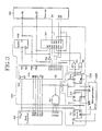
- the document data input system comprises a host computer 100 for controlling the operation of the whole system and storing scanned data to its hard disk; a scanner 200 for scanning document data; a scanner interface unit 300, associated with the host computer 100 and the scanner 200, for executing an interface operation therebetween upon the control of the host computer 100; a microprocessor 400 associated with a global memory 401 and a local memory 402; and an interface unit 310 for latching scanned data passed through the scanner interface unit 300 upon the control of the host computer 100 and applying the latched data to the microprocessor 400.
- Fig. 3 shows in detail the scanner interface unit and the interface unit.
- the scanner interface unit 300 is constituted in such a manner that data ports D0-D7, read control signal port IOR , write control signal port IWO , selection signal ports SA0 and SA1, and reset signal port RSD of the host computer 100 are connected respectively to data ports D0-D7, read port RD , write port WR , selection ports A0 and A1, an d reset port RS of a scanner interface 302, and also input/output signal ports IO0-IO3 of the host computer 100 are connected to a chip selection port CS of the scanner interface 302 via an AND gate 301, output ports PA0-PA7 of the scanner interface 302 are connected via a buffer 303 to data ports D1-D8 of the scanner 200 and input ports PB0-PB7 of the scanner interface 302 directly to the data ports D1-D8 of the scanner 200; a mode control signal port PC4 of the scanner interface 302 is connected to a preset/scanner port PR/ SC of
- the interface unit 310 is constituted in such a manner that data ports D0-D7 of the scanner interface 302 are connected to data ports D0-D7 of the latch 312 and output ports Q0-Q7 of the latch 312 are connected to data ports D0-D0-D7 of the microprocessor 400; input/output signal port IO1 of the host computer 100 is connected to a clock port CK of the latch 312, a clear port CL of a flip-flop 313, and a preset port PS of a flip-flop 314 and also a reset signal port RSD of the host computer 100 is connected via the inverter 311 to the preset port PS of the flip-flop 313 and the clear terminal CL of the flip-flop 314; the output port Q of the flip-flop 313 is connected to an interrupt port INT of the microprocessor 400 and interrupt acknowledge signal port IACK , output demand signal port P6 and completion signal port P5 of the microprocessor 400 are connected to the clock port CK of the flip-flop 313, the output enable port OE of the latch 312
- the scanner interface 302 is a programmable peripheral interface (PPI) which is structured such that its data ports D0-D7 are selectively connected to its output ports PA0-PA7, input ports PB0-PB7 and control ports PC0-PC7 in response to signals being applied to its selection ports A0 and A1, and the multiplexer 307 is structured such that its ports 1A1-1A3 are connected to its ports 1Y1 -1Y3 when a low potential signal is applied to its enable port 1G , and its ports 2A2 and 2A3 are connected to its ports 2Y2 and 2Y3 when a low potential signal is applied to its enable port 2G .
- PPI programmable peripheral interface
- the host computer 100 outputs a low level signal at its input/output port IO2, a low level signal is outputted from the AND gate 301, thereby causing the scanner interface 302 to be enabled. And at the selection signal port SA0 of the host computer 100, a low level signal is outputted and at the selection signal port SA1 thereof, a high level signal is outputted, thereby the control ports PC0-PC7 of the scanner interface 302 are selected. At this moment, the host computer 100 outputs preset mode data at its data ports D0-D7 so that high level preset mode signals are outputted from the mode control signal port PC4 of the scanner interface 302.
- the high level preset mode signal is applied to the preset/scanner port PR/ SC of the scanner 200, thereby causing the scanner 200 to be a preset mode, and since the high level preset mode signal is inverted into a low level signal at the inverter 304, the buffer 303 is enabled so that the input port A thereof is connected to its output port Y, and the input ports 1A1-1A3 of the multiplexer 307 are connected to the output ports 1Y1-1Y3 thereof.
- the host computer 100 outputs a low level signal at its input/output port IO0, thereby causing the scanner interface 302 to be enabled and at the selection signal ports SA0 and SA1 thereof, low level signals are outputted, thereby causing the output ports PA0-PA7 of the scanner interface 302 to be selected, and then the scanner interface 302 becomes a write state by the low level write signal being outputted from the write signal port IOW of the host computer 100.
- the scanner interface 302 receives through its data ports D0-D7 as an input the data being outputted from the data ports D0-D7 of the host computer 100 and outputs them through its output ports PA0-PA7, and the data from the output ports PA0-PA7 of the scanner interface 302 are applied to the data ports D1-D8 of the scanner 200 through the buffer 303.
- low level signals are outputted from the interrupt signal port PC3 and output buffer full port PC7 of the scanner interface 302 and the low level signals are applied to the busy port BY and strobe port ST of the scanner 200 through the ports 1A3, 1Y3 and 1A1, 1Y1 of the multiplexer 307, thereby the scanner 200 receives and processes the data being applied to its data ports D1-D8.
- a low level interrupt acknowledge signal is outputted through its port RS and since this low level interrupt acknowledge signal is applied via ports 1A2 and 1Y2 of the multiplexer 307 to the acknowledge port PC6 of the scanner interface 302, a high level signal is outputted from the interrupt signal port PC3 and output buffer full port PC7 thereof at the time that the low level acknowledge signal becomes a high level signal, thereby causing the scanner interface 302 to be initialized.
- the host computer 100 selects the control ports PC0-PC7 of the scanner interface 302, as above described, to identify that the scanner 200 read the data by checking the condition of the acknowledge port PC6. That is, at this time, when the acknowledge port PC6 is in a high level state, it means that the scanner 200 read the data, so that the host computer 100 may record the data in the scanner interface 302.
- a low level signal is outputted from the input/output port IO2 of the host computer 100, thereby causing the scanner interface 302 to be enabled, and a low level signal is outputted from the selection signal port SA0 of the host computer 100 and a high level signal is outputted from the selection signal port SA1 so that the control ports PC0-PC7 of the scanner interface 302 are selected.
- scanner mode data are outputted from the data ports D0-D7 of the host computer 100 so that a low level scanner mode signal is outputted from the mode control signal port PC4 of the scanner interface 302.
- This low level scanner mode signal is applied to the preset/scanner port PR/ SC of the scanner 200, thereby causing the scanner 200 to be in a scanner mode, and since the low level scanner mode signal is inverted into a high level signal at the inverter 304, the buffer 303 is disabled and the multiplexer 307 is in a state that its input ports 2A2 and 2A3 are connected to the output ports 2Y2 and 2Y3 thereof.
- a low level signal is outputted from the strobe port ST of the scanner and applied to one side input port of the OR gate 305 through the ports 2A2 and 2Y2 of the multiplexer 307 and also a low level signal is outputted from the output port Q of the flip-flop 314, so that a low level signal is outputted from the OR gate 305 and applied to the strobe port PC2 of the scanner interface 302, thereby a high level signal is outputted from the input buffer full port PC1 of the scanner interface 302.
- This high level signal is applied via the OR gate 306 and the ports 2A3 and 2Y3 of the multiplexer 307 to the busy port BY of the scanner 200 so that the scanner 200 does not transmit data.
- the host computer 100 selects the control ports PC0-PC7 of the scanner interface 302, as described above, and checks the condition of the strobe port PC2 and then reads, when the strobe port PC2 is in a low level state, the data inputted in the input ports PB0-PB7.
- a low level signal is outputted from the input/output port IO1 of the host computer 100, thereby causing the scanner interface 302 to be enabled, and also a high level signal is outputted from the selection signal port SA0 and a low level signal is outputted from the selection signal port SA1, thereby causing the input ports PB0-PB7 of the scanner interface 302 to be selected.
- the scanner interface 302 becomes a read state by the low level read signal being outputted at the read signal port IOR of the host computer 100, thereby the data inputted in the input ports PB0-PB7 of the scanner interface 302 are outputted through the data ports D0-D7 and then stroed in the hard disk.
- the low level signal being outputted from the input/output port IO1 of the host computer 100 is applied to the clock port CK of the latch 312 as a clock signal, the data outputted at the data ports D0-D7 of the scanner interface 302 are latched at the latch 312, and a low level signal outputted at the input/output port IO1 of the host computer 100 causes the flip-flop 313 to be cleared so as to output a low level signal through its output port Q and the flip-flop 314 to be preset so as to output a high level signal through its output port Q.
- the low level signal outputted at the output port Q of the flip-flop 313 is applied to the interrupt port INT of the microprocessor 400 as an interrupt signal, thereby the micrcprocessor 400 outputs a low level interrupt acknowledge signal through its interrupt acknowledge signal port IACK so that a high level signal is outputted again at the output port Q of the flip-flop 313. And, at this moment the microprocessor 400 outputs a low level output demand signal through its output demand signal port P6 so that the latch 312 is to be enabled, and then the data latched at the latch 312 are cutputted through its output ports Q0-Q7 and applied to the data ports D0-D7 of the microprocessor 400.
- the microprocessor 400 stroes the data being applied to its data ports D0-D7 to the global memory 401 and compresses the data in accordance with the user's processing program and then stroes the compressed data to the local memory 402.
- the microprocessor 400 After completing the process of data at the microprocessor 400, the microprocessor 400 outputs a low level completion signal through its completion signal port P5 and applies the signal to the clock port CK of the flip-flop 314. At this time, since the flip-flop 314 outputs a low level signal through its output port Q, then the scanner 200 is ready to transmit the next pixel data.
- the scanned data when scanned data are stored via a scanner interface unit to a hard disk of a host computer, the scanned data are latched at a latch and stored to another microprocessor, and until the microprocessor finishes the process of the scanned data, the scanner does not transmit the next pixel data, so that the reliability of the product and the using efficiency of the host computer can be enhanced.
- the present invention is applicable to a document acknowledge system comprising a multiprocessor.
Abstract
Description
- The present invention relates to a document data input system which receives data scanned at a scanner and stores the scanned data in a hard disk of a host computer, and more particularly to a document data input system for a scanner which is designed to be suitably used for a document acknowledge system comprising a multiprocessor.
- A conventional scanner interface, which is shown in Fig. 1, comprises a
host computer 10 which receives data scanned at ascanner 12 via ascanner interface unit 11 and then stores the data in its internal hard disk. - In such a conventional system, the
host computer 10 sets a mode of thescanner interface unit 11 by means of a register value and receives data scanned at thescanner 12 as an input via thescanner interface unit 11, and then stores the inputted data to a hard disk. Thereafter, the data stored in the hard disk are processed by thehost computer 10 in accordance with the user's intention. - However, in such a conventional system there has been the drawback that since the scanned data are stored only in the hard disk of the host computer, the data stored in the hard disk should be transmitted from the host computer to other processor in case that the data are needed by other processor, and it takes not a few times to transmit the data at the host computer, causing the processing efficiency to be lowered.
- Therefore, it is an object of the present invention to provide a document data input system for a scanner which can input the data scanned at the scanner to another microprocessor and store them to a buffer memory when inputting the scanned data to a host computer and storing to its hard disk.
- The object of the present invention is attained by providing a document data input system which is constituted such that data transmitted from a host computer are applied to a scanner via an interface unit upon the control of the host computer, data scanned at the scanner are applied via the interface unit to the host computer by a read control signal of the host computer and then latched at a latch, and the latched data are read by the microprocessor and thereafter a completion signal is applied to the scanner.
- The above and other objects, features and advantages of the invention will be clearly understood from the following detailed description taken in conjunction with the accompanying drawings, wherein:
- Fig. 1 is a diagram showing the configuration of a scanner interface according to a prior art system;
- Fig. 2 a block diagram showing the configuration of a document data input system of the present invention; and
- Fig. 3 is a detailed circuit diagram of the scanner interface unit of Fig. 2.
- Referring to Fig. 2, the document data input system according to the present invention comprises a
host computer 100 for controlling the operation of the whole system and storing scanned data to its hard disk; ascanner 200 for scanning document data; ascanner interface unit 300, associated with thehost computer 100 and thescanner 200, for executing an interface operation therebetween upon the control of thehost computer 100; amicroprocessor 400 associated with aglobal memory 401 and alocal memory 402; and aninterface unit 310 for latching scanned data passed through thescanner interface unit 300 upon the control of thehost computer 100 and applying the latched data to themicroprocessor 400. - Fig. 3 shows in detail the scanner interface unit and the interface unit. As shown in Fig. 3, the
scanner interface unit 300 is constituted in such a manner that data ports D₀-D₇, read control signal portIOR , write control signal portIWO , selection signal ports SA₀ and SA₁, and reset signal port RSD of thehost computer 100 are connected respectively to data ports D₀-D₇, read portRD , write portWR , selection ports A₀ and A₁, an d reset port RS of ascanner interface 302, and also input/output signal ports IO₀-IO₃ of thehost computer 100 are connected to a chip selection portCS of thescanner interface 302 via anAND gate 301, output ports PA₀-PA₇ of thescanner interface 302 are connected via abuffer 303 to data ports D₁-D₈ of thescanner 200 and input ports PB₀-PB₇ of thescanner interface 302 directly to the data ports D₁-D₈ of thescanner 200; a mode control signal port PC₄ of thescanner interface 302 is connected to a preset/scanner port PR/SC of thescanner 200 and an enableport 2G of amultiplexer 307 as well as to an enable portG of thebuffer 303 and an enable port1G of themultiplexer 307 via aninverter 304; interrupt signal port PC₃, acknowledge port PC₆, and output buffer full port PC₇ of thescanner interface 302 are connected to ports 1A₃, 1Y₂ and 1A₁ of themultiplexer 307, in put buffer full port IC₁ via anOR gate 306 to a port 2A₃ of themultiplexer 307, and also ports 1Y₃ and 2Y₃, 1A₂ and 1Y₁ to ports BY, RS and ST of thescanner 200; and then the port ST is connected to a port 2A₂ of themultiplexer 307 and also the port 2Y₂ via anOR gate 305 to a strobe port PC₂ of thescanner interface 302. Meanwhile, theinterface unit 310 is constituted in such a manner that data ports D₀-D₇ of thescanner interface 302 are connected to data ports D₀-D₇ of thelatch 312 and output ports Q₀-Q₇ of thelatch 312 are connected to data ports D₀-D₀-D₇ of themicroprocessor 400; input/output signal port IO₁ of thehost computer 100 is connected to a clock port CK of thelatch 312, a clear portCL of a flip-flop 313, and a preset portPS of a flip-flop 314 and also a reset signal port RSD of thehost computer 100 is connected via theinverter 311 to the preset portPS of the flip-flop 313 and the clear terminalCL of the flip-flop 314; the output port Q of the flip-flop 313 is connected to an interrupt portINT of themicroprocessor 400 and interrupt acknowledge signal portIACK , output demand signal port P₆ and completion signal port P₅ of themicroprocessor 400 are connected to the clock port CK of the flip-flop 313, the output enable portOE of thelatch 312 and the clock port CK of the flip-flop 314; and the output port Q of the flip-flop 314 is connected to inputs ofOR gates scanner interface 302 is a programmable peripheral interface (PPI) which is structured such that its data ports D₀-D₇ are selectively connected to its output ports PA₀-PA₇, input ports PB₀-PB₇ and control ports PC₀-PC₇ in response to signals being applied to its selection ports A₀ and A₁, and themultiplexer 307 is structured such that its ports 1A₁-1A₃ are connected to its ports 1Y₁ -1Y₃ when a low potential signal is applied to its enable port1G , and its ports 2A₂ and 2A₃ are connected to its ports 2Y₂ and 2Y₃ when a low potential signal is applied to its enableport 2G . - Hereinafter, the operation and effect of the present invention will be described in detail.
- When a high level reset signal is applied from the reset signal port RSD of the
host computer 100 to the reset port RS of thescanner interface 302; thescanner interface 302 is reset and initialized. At this time, since the high level reset signal is inverted into a low level signal at theinverter 311, the flip-flip 313 is preset to output a high level signal from its output port Q and the flip-flop 314 is cleared to output a low level signal from its output terminal Q, whereby output signals of theOR gates multiplexer 307 and of the strobe port PC₂ of thescanner interface 302. - Under these conditions, when the
host computer 100 outputs a low level mode selection control signal at its input/output signal port I03, a low level signal is outputted from theAND gate 301, thereby causing thescanner interface 302 to be enabled, and at this time thehost computer 100 outputs mode data AO (Hex) through its data ports D₀-D₇ to set thescanner interface 302 to a strobe input/output mode. - Thereafter, as the
host computer 100 outputs a low level signal at its input/output port IO₂, a low level signal is outputted from theAND gate 301, thereby causing thescanner interface 302 to be enabled. And at the selection signal port SA₀ of thehost computer 100, a low level signal is outputted and at the selection signal port SA₁ thereof, a high level signal is outputted, thereby the control ports PC₀-PC₇ of thescanner interface 302 are selected. At this moment, thehost computer 100 outputs preset mode data at its data ports D₀-D₇ so that high level preset mode signals are outputted from the mode control signal port PC₄ of thescanner interface 302. The high level preset mode signal is applied to the preset/scanner port PR/SC of thescanner 200, thereby causing thescanner 200 to be a preset mode, and since the high level preset mode signal is inverted into a low level signal at theinverter 304, thebuffer 303 is enabled so that the input port A thereof is connected to its output port Y, and the input ports 1A₁-1A₃ of themultiplexer 307 are connected to the output ports 1Y₁-1Y₃ thereof. At this time, thehost computer 100 outputs a low level signal at its input/output port IO₀, thereby causing thescanner interface 302 to be enabled and at the selection signal ports SA₀ and SA₁ thereof, low level signals are outputted, thereby causing the output ports PA₀-PA₇ of thescanner interface 302 to be selected, and then thescanner interface 302 becomes a write state by the low level write signal being outputted from the write signal portIOW of thehost computer 100. - Thus, the
scanner interface 302 receives through its data ports D₀-D₇ as an input the data being outputted from the data ports D₀-D₇ of thehost computer 100 and outputs them through its output ports PA₀-PA₇, and the data from the output ports PA₀-PA₇ of thescanner interface 302 are applied to the data ports D₁-D₈ of thescanner 200 through thebuffer 303. - And, at the time that the low level write signal is inverted into a high level signal, low level signals are outputted from the interrupt signal port PC₃ and output buffer full port PC₇ of the
scanner interface 302 and the low level signals are applied to the busy port BY and strobe port ST of thescanner 200 through the ports 1A₃, 1Y₃ and 1A₁, 1Y₁ of themultiplexer 307, thereby thescanner 200 receives and processes the data being applied to its data ports D₁-D₈. - After the data are inputted to the
scanner 200, a low level interrupt acknowledge signal is outputted through its port RS and since this low level interrupt acknowledge signal is applied via ports 1A₂ and 1Y₂ of themultiplexer 307 to the acknowledge port PC₆ of thescanner interface 302, a high level signal is outputted from the interrupt signal port PC₃ and output buffer full port PC₇ thereof at the time that the low level acknowledge signal becomes a high level signal, thereby causing thescanner interface 302 to be initialized. - In this state, the
host computer 100 selects the control ports PC₀-PC₇ of thescanner interface 302, as above described, to identify that thescanner 200 read the data by checking the condition of the acknowledge port PC₆. That is, at this time, when the acknowledge port PC₆ is in a high level state, it means that thescanner 200 read the data, so that thehost computer 100 may record the data in thescanner interface 302. - When the
host computer 100 finishes to transmit all the data to thescanner 200 via thescanner interface 302, a low level signal is outputted from the input/output port IO₂ of thehost computer 100, thereby causing thescanner interface 302 to be enabled, and a low level signal is outputted from the selection signal port SA₀ of thehost computer 100 and a high level signal is outputted from the selection signal port SA₁ so that the control ports PC₀-PC₇ of thescanner interface 302 are selected. At this moment, scanner mode data are outputted from the data ports D₀-D₇ of thehost computer 100 so that a low level scanner mode signal is outputted from the mode control signal port PC₄ of thescanner interface 302. This low level scanner mode signal is applied to the preset/scanner port PR/SC of thescanner 200, thereby causing thescanner 200 to be in a scanner mode, and since the low level scanner mode signal is inverted into a high level signal at theinverter 304, thebuffer 303 is disabled and themultiplexer 307 is in a state that its input ports 2A₂ and 2A₃ are connected to the output ports 2Y₂ and 2Y₃ thereof. - In case that the
scanner 200 outputs data through its data ports D₁-D₈ to the input ports PB₀-PB₇ of thescanner interface 302, a low level signal is outputted from the strobe port ST of the scanner and applied to one side input port of theOR gate 305 through the ports 2A₂ and 2Y₂ of themultiplexer 307 and also a low level signal is outputted from the output port Q of the flip-flop 314, so that a low level signal is outputted from theOR gate 305 and applied to the strobe port PC₂ of thescanner interface 302, thereby a high level signal is outputted from the input buffer full port PC₁ of thescanner interface 302. This high level signal is applied via the ORgate 306 and the ports 2A₃ and 2Y₃ of themultiplexer 307 to the busy port BY of thescanner 200 so that thescanner 200 does not transmit data. At this moment, thehost computer 100 selects the control ports PC₀-PC₇ of thescanner interface 302, as described above, and checks the condition of the strobe port PC₂ and then reads, when the strobe port PC₂ is in a low level state, the data inputted in the input ports PB₀-PB₇. - That is, at this time, a low level signal is outputted from the input/output port IO₁ of the
host computer 100, thereby causing thescanner interface 302 to be enabled, and also a high level signal is outputted from the selection signal port SA₀ and a low level signal is outputted from the selection signal port SA₁, thereby causing the input ports PB₀-PB₇ of thescanner interface 302 to be selected. At this time, thescanner interface 302 becomes a read state by the low level read signal being outputted at the read signal port IOR of thehost computer 100, thereby the data inputted in the input ports PB₀-PB₇ of thescanner interface 302 are outputted through the data ports D₀-D₇ and then stroed in the hard disk. - In addition, since the low level signal being outputted from the input/output port IO₁ of the
host computer 100 is applied to the clock port CK of thelatch 312 as a clock signal, the data outputted at the data ports D₀-D₇ of thescanner interface 302 are latched at thelatch 312, and a low level signal outputted at the input/output port IO₁ of thehost computer 100 causes the flip-flop 313 to be cleared so as to output a low level signal through its output port Q and the flip-flop 314 to be preset so as to output a high level signal through its output port Q. - The low level signal outputted at the output port Q of the flip-
flop 313 is applied to the interrupt portINT of themicroprocessor 400 as an interrupt signal, thereby themicrcprocessor 400 outputs a low level interrupt acknowledge signal through its interrupt acknowledge signal portIACK so that a high level signal is outputted again at the output port Q of the flip-flop 313. And, at this moment themicroprocessor 400 outputs a low level output demand signal through its output demand signal port P₆ so that thelatch 312 is to be enabled, and then the data latched at thelatch 312 are cutputted through its output ports Q₀-Q₇ and applied to the data ports D₀-D₇ of themicroprocessor 400. Thus themicroprocessor 400 stroes the data being applied to its data ports D₀-D₇ to theglobal memory 401 and compresses the data in accordance with the user's processing program and then stroes the compressed data to thelocal memory 402. - After completing the process of data at the
microprocessor 400, themicroprocessor 400 outputs a low level completion signal through its completion signal port P₅ and applies the signal to the clock port CK of the flip-flop 314. At this time, since the flip-flop 314 outputs a low level signal through its output port Q, then thescanner 200 is ready to transmit the next pixel data. - That is, while a low level signal is outputted at the input buffer full port PC₁ of the
scanner interface 302 at the time that a low level read signal outputted at the read signal portIOR of thehost computer 100 is turned to a high level signal, a high level signal is already outputted at the output port Q of the flip-flop 314 as above described, so that a high level signal is outputted from the ORgate 306 and applied continuously to the busy port BY of thescanner 200, thereby thescanner 200 can not transmit the next pixel data. Thereafter, when a low level signal is outputted at the flip-flop 314 as above described, a low level signal is outputted from the ORgate 306 and applied to the busy port BY of thescanner 200, thereby thescanner 200 then can transmit the next pixel data. - As described above in detail, in accordance with the present invention, when scanned data are stored via a scanner interface unit to a hard disk of a host computer, the scanned data are latched at a latch and stored to another microprocessor, and until the microprocessor finishes the process of the scanned data, the scanner does not transmit the next pixel data, so that the reliability of the product and the using efficiency of the host computer can be enhanced. Also, the present invention is applicable to a document acknowledge system comprising a multiprocessor.
Claims (3)
- A document data input system for a scanner, comprising;
a host computer for controlling the whole operation of the system and receiving and storing scanned data to a hard disk;
a scanner for scanning document data;
a scanner interface unit for carrying out a data interface operation between the host computer and the scanner, upon the control of the host computer;
a microprocessor associated with a global memory and a local memory; an d
an interface unit for latching the scanned data passed through the scanner interface unit upon the control of the host computer and applying the latched data to the microprocessor upon the control of the microprocessor and then applying a completion signal to the scanner interface unit when the data input to the microprocessor is completed. - The document data input system for a scanner as claimed in claim 1, wherein the scanner interface unit is constituted such that data ports D₀-D₇, read control signal port
IOR , write control signal portIWO , selection signal ports SA₀ and SA₁, and reset signal port RSD of the host computer are connected respectively to data ports D₀-D₇, read portRD , write portWR , selection ports A₀ and A₁, and reset port RS of a scanner interface and also input/output signal ports IO₀-IO₃ of the host computer are connected to a chip selection port CS of the scanner interface via an AND gate , output ports PA₀-PA₇ of the scanner interface are connected via a buffer to data ports D₁-D₈ of the scanner together with the input ports PB₀-PB₇ thereof, to the data ports D₁-D₈ of the scanner; a mode control signal port PC₄ of the scanner interface is connected to a preset/scanner port PR/SC of the scanner and an enable port2G of a multiplexer as well as to an enable portG of the buffer and an enable port1G of the multiplexer via an inverter; interrupt signal port PC₃, acknowledge port PC₆, and output buffer full port PC₇ of the scanner interface are connected to ports 1A₃, 1Y₂ and 1A₁ of the multiplexer, input buffer full port IC₁ via an OR gate to a port 2A₃ of the multiplexer, and also ports 1Y₃ and 2Y₃, 1A₂ and 1Y₁ to ports BY, RS and ST of the scanner ; and then the port ST of the scanner is connected to a port 2A₂ of the multiplexer and also the port 2Y₂ via an OR gate to a strobe port PC₂ of the scanner interface. - The document data input system for a scanner as claimed in claim 1, wherein the interface unit is constituted such that data ports D₀-D₇ of the host computer are connected to data ports D₀-D₇ of the latch, a reset signal port RSD of the host computer is connected via an inverter to a preset port PS of the first flip-flop and to a clear port
CL of the second flip-flop, an input/ouput port IO₁ of the host computer is connected to a clock port CK of the latch, a clear portCL of the first flip-flop, and a preset portPS of the second flip-flop, an output port Q of the first flip-flop is connected to an interrupt portINT of the microprocessor, an output demand signal port P₆ and data ports D₀-d₇ of the microprocessor are connected respectively to an output enable portOE and output ports Q₀-Q₇ of the latch, and an interrupt acknowledge signal portIACK and a completion signal port P₅ of the microprocessor are connected respectively to clock ports CK and CK of the first and second flip-flops.
Applications Claiming Priority (2)
| Application Number | Priority Date | Filing Date | Title |
|---|---|---|---|
| KR736090 | 1990-05-22 | ||
| KR1019900007360A KR930000012B1 (en) | 1990-05-22 | 1990-05-22 | Data input apparatus of scanner |
Publications (3)
| Publication Number | Publication Date |
|---|---|
| EP0458693A2 true EP0458693A2 (en) | 1991-11-27 |
| EP0458693A3 EP0458693A3 (en) | 1992-04-22 |
| EP0458693B1 EP0458693B1 (en) | 1995-12-13 |
Family
ID=19299293
Family Applications (1)
| Application Number | Title | Priority Date | Filing Date |
|---|---|---|---|
| EP91401303A Expired - Lifetime EP0458693B1 (en) | 1990-05-22 | 1991-05-21 | Document data input system for a scanner |
Country Status (5)
| Country | Link |
|---|---|
| US (1) | US5432914A (en) |
| EP (1) | EP0458693B1 (en) |
| JP (1) | JPH05114021A (en) |
| KR (1) | KR930000012B1 (en) |
| DE (1) | DE69115351T2 (en) |
Cited By (1)
| Publication number | Priority date | Publication date | Assignee | Title |
|---|---|---|---|---|
| EP0576226A3 (en) * | 1992-06-22 | 1994-02-16 | Fujitsu Ltd |
Families Citing this family (10)
| Publication number | Priority date | Publication date | Assignee | Title |
|---|---|---|---|---|
| US6786420B1 (en) | 1997-07-15 | 2004-09-07 | Silverbrook Research Pty. Ltd. | Data distribution mechanism in the form of ink dots on cards |
| US6618117B2 (en) | 1997-07-12 | 2003-09-09 | Silverbrook Research Pty Ltd | Image sensing apparatus including a microcontroller |
| US7551201B2 (en) | 1997-07-15 | 2009-06-23 | Silverbrook Research Pty Ltd | Image capture and processing device for a print on demand digital camera system |
| US7110024B1 (en) | 1997-07-15 | 2006-09-19 | Silverbrook Research Pty Ltd | Digital camera system having motion deblurring means |
| US6879341B1 (en) | 1997-07-15 | 2005-04-12 | Silverbrook Research Pty Ltd | Digital camera system containing a VLIW vector processor |
| US6690419B1 (en) | 1997-07-15 | 2004-02-10 | Silverbrook Research Pty Ltd | Utilising eye detection methods for image processing in a digital image camera |
| US6624848B1 (en) | 1997-07-15 | 2003-09-23 | Silverbrook Research Pty Ltd | Cascading image modification using multiple digital cameras incorporating image processing |
| US6429952B1 (en) | 1998-08-31 | 2002-08-06 | Sharp Laboratories Of America | Browser interface to scanner |
| AUPQ056099A0 (en) | 1999-05-25 | 1999-06-17 | Silverbrook Research Pty Ltd | A method and apparatus (pprint01) |
| US6618771B1 (en) * | 2000-02-16 | 2003-09-09 | Hewlett-Packard Development Company, Lp. | Method and apparatus for use in installing a scanner |
Citations (2)
| Publication number | Priority date | Publication date | Assignee | Title |
|---|---|---|---|---|
| US3558811A (en) * | 1967-05-25 | 1971-01-26 | Xerox Corp | Graphic communication electrical interface system |
| EP0042071A2 (en) * | 1980-05-21 | 1981-12-23 | Siemens Aktiengesellschaft | Multiple-purpose terminal connected to a data processing apparatus or a text editing automat |
Family Cites Families (7)
| Publication number | Priority date | Publication date | Assignee | Title |
|---|---|---|---|---|
| US5038298A (en) * | 1986-03-14 | 1991-08-06 | Canon Kabushiki Kaisha | Image output apparatus connectable to mutually different external data processing apparatus |
| US5019916A (en) * | 1987-05-09 | 1991-05-28 | Ricoh Company, Ltd. | Digital copier with a facsimile function |
| JP2740180B2 (en) * | 1987-05-09 | 1998-04-15 | 株式会社リコー | Copier |
| US5153746A (en) * | 1988-03-10 | 1992-10-06 | Kabushiki Kaisha Toshiba | Document processing apparatus with facsimile function |
| JPH0626411B2 (en) * | 1988-05-19 | 1994-04-06 | ニスカ株式会社 | Image reading device interface circuit |
| US5167021A (en) * | 1988-09-19 | 1992-11-24 | Ncr Corporation | Multimedia interface device and method |
| KR920001182B1 (en) * | 1989-02-28 | 1992-02-06 | 삼성전자 주식회사 | Multy-copy method for fax |
-
1990
- 1990-05-22 KR KR1019900007360A patent/KR930000012B1/en not_active IP Right Cessation
-
1991
- 1991-05-21 DE DE69115351T patent/DE69115351T2/en not_active Expired - Fee Related
- 1991-05-21 US US07/703,481 patent/US5432914A/en not_active Expired - Fee Related
- 1991-05-21 EP EP91401303A patent/EP0458693B1/en not_active Expired - Lifetime
- 1991-05-22 JP JP3117284A patent/JPH05114021A/en not_active Withdrawn
Patent Citations (2)
| Publication number | Priority date | Publication date | Assignee | Title |
|---|---|---|---|---|
| US3558811A (en) * | 1967-05-25 | 1971-01-26 | Xerox Corp | Graphic communication electrical interface system |
| EP0042071A2 (en) * | 1980-05-21 | 1981-12-23 | Siemens Aktiengesellschaft | Multiple-purpose terminal connected to a data processing apparatus or a text editing automat |
Non-Patent Citations (2)
| Title |
|---|
| * PAGES 98,99 ; CHAPTER 6 * * |
| 1982 INTERNATIONAL ZURICH SEMINAR ON DIGITAL COMMUNICATION , MAN-MACHINE INTERACTION , MARCH9-11,1982 ZURICH/SWITZERLAND pages 93 - 100; W.HORAK: 'EXPERIMENTAL TEXT AND FACSIMILE INTEGRATED WORKSTATION' * |
Cited By (4)
| Publication number | Priority date | Publication date | Assignee | Title |
|---|---|---|---|---|
| EP0576226A3 (en) * | 1992-06-22 | 1994-02-16 | Fujitsu Ltd | |
| US5517331A (en) * | 1992-06-22 | 1996-05-14 | Fujitsu Limited | Method and apparatus for reading image of image scanner-reader |
| EP0804016A2 (en) * | 1992-06-22 | 1997-10-29 | Fujitsu Limited | Method and apparatus for reading image of image scanner-reader |
| EP0804016A3 (en) * | 1992-06-22 | 1998-11-18 | Fujitsu Limited | Method and apparatus for reading image of image scanner-reader |
Also Published As
| Publication number | Publication date |
|---|---|
| KR910020541A (en) | 1991-12-20 |
| JPH05114021A (en) | 1993-05-07 |
| US5432914A (en) | 1995-07-11 |
| DE69115351D1 (en) | 1996-01-25 |
| DE69115351T2 (en) | 1996-05-09 |
| EP0458693A3 (en) | 1992-04-22 |
| EP0458693B1 (en) | 1995-12-13 |
| KR930000012B1 (en) | 1993-01-06 |
Similar Documents
| Publication | Publication Date | Title |
|---|---|---|
| EP0189638B1 (en) | Bus width adapter | |
| US4271466A (en) | Direct memory access control system with byte/word control of data bus | |
| EP0458693A2 (en) | Document data input system for a scanner | |
| US6397285B1 (en) | Image input device employing a personal computercard/interface or generic interface | |
| US5163145A (en) | Circuit for determining between a first or second type CPU at reset by examining upper M bits of initial memory reference | |
| EP0408353B1 (en) | Semiconductor integrated circuit | |
| JP2527251B2 (en) | IC card | |
| US5303366A (en) | Interface card for scanner | |
| JP2719419B2 (en) | IC card | |
| US5479165A (en) | Two-dimensional coding apparatus | |
| JP2748537B2 (en) | Denormalized data processor | |
| JP2884620B2 (en) | Digital image processing device | |
| KR870000834Y1 (en) | Interface for microprocessor | |
| KR20010063803A (en) | Multimedia Card(MMC) To Support The Video Codec Function | |
| JP2830239B2 (en) | Input display control device | |
| RU2024051C1 (en) | Data source-to-processor interface | |
| JPH01240990A (en) | Slip reading processor | |
| JPS62241041A (en) | Information processor | |
| JPS6116094B2 (en) | ||
| JPH0758504B2 (en) | Image input device | |
| JPH0421024A (en) | Automatic initializing circuit for video interface | |
| JPH0816507A (en) | Peripheral device for ide bus | |
| JPH04352045A (en) | Connecting device for ic card | |
| JPH01113875A (en) | Image input device | |
| JPH05120879A (en) | Semiconductor memory device |
Legal Events
| Date | Code | Title | Description |
|---|---|---|---|
| PUAI | Public reference made under article 153(3) epc to a published international application that has entered the european phase |
Free format text: ORIGINAL CODE: 0009012 |
|
| AK | Designated contracting states |
Kind code of ref document: A2 Designated state(s): DE FR |
|
| PUAL | Search report despatched |
Free format text: ORIGINAL CODE: 0009013 |
|
| AK | Designated contracting states |
Kind code of ref document: A3 Designated state(s): DE FR |
|
| 17P | Request for examination filed |
Effective date: 19920706 |
|
| 17Q | First examination report despatched |
Effective date: 19940422 |
|
| RAP1 | Party data changed (applicant data changed or rights of an application transferred) |
Owner name: LG ELECTRONICS INC. |
|
| GRAA | (expected) grant |
Free format text: ORIGINAL CODE: 0009210 |
|
| AK | Designated contracting states |
Kind code of ref document: B1 Designated state(s): DE FR |
|
| REF | Corresponds to: |
Ref document number: 69115351 Country of ref document: DE Date of ref document: 19960125 |
|
| ET | Fr: translation filed | ||
| PLBE | No opposition filed within time limit |
Free format text: ORIGINAL CODE: 0009261 |
|
| STAA | Information on the status of an ep patent application or granted ep patent |
Free format text: STATUS: NO OPPOSITION FILED WITHIN TIME LIMIT |
|
| 26N | No opposition filed | ||
| PGFP | Annual fee paid to national office [announced via postgrant information from national office to epo] |
Ref country code: DE Payment date: 20010514 Year of fee payment: 11 |
|
| PGFP | Annual fee paid to national office [announced via postgrant information from national office to epo] |
Ref country code: FR Payment date: 20010518 Year of fee payment: 11 |
|
| PG25 | Lapsed in a contracting state [announced via postgrant information from national office to epo] |
Ref country code: DE Free format text: LAPSE BECAUSE OF NON-PAYMENT OF DUE FEES Effective date: 20021203 |
|
| PG25 | Lapsed in a contracting state [announced via postgrant information from national office to epo] |
Ref country code: FR Free format text: LAPSE BECAUSE OF NON-PAYMENT OF DUE FEES Effective date: 20030131 |
|
| REG | Reference to a national code |
Ref country code: FR Ref legal event code: ST |